如何從零開始設計 ESP32-S3 開發板:4 層 PCB 設計教學
8 分鐘
- Custom ESP32-S3 Development Board 硬體規格
- Step 1:設計 ESP32-S3 Development Board 原理圖
- Step 2:規劃 ESP32-S3 Development Board 的 4-Layer PCB Stack-Up
- Step 3:進行 PCB Component Placement
- Step 4:Routing ESP32-S3 PCB
- Step 5:加入 Ground Copper Pour 與 Via Stitching
- Step 6:進行最終 PCB Check 與 Design Rule Check(DRC)
- Step 7:產生 ESP32-S3 PCB Manufacturing File
- Step 8:透過 JLCPCB 製作 ESP32-S3 Development Board
- Step 9:組裝 ESP32-S3 Development Board
- ESP32-S3 Development Board PCB 製造流程
- 結論
- ESP32-S3 PCB Design 常見問題
自行設計 ESP32-S3 Development Board,可以讓您完整掌控 Hardware Architecture,同時為 IoT Project 後續進入 Commercial Production 做好準備。
相較直接使用體積較大的 Off-the-Shelf Development Board,Custom Design 可以讓您:
- 最佳化 PCB Board Space
- 只引出實際需要的 GPIO
- 將 Peripheral 直接整合到同一塊 PCB
- 依實際產品需求規劃 Power、USB、Protection 與 Connector
本教學將從零開始設計一塊 4-Layer ESP32-S3 Development Board。
我們將完整介紹 Hardware Development Pipeline,包括 ESP32-S3 Schematic 架構、4-Layer PCB Stack-Up 規劃、PCB Routing Best Practices,以及如何準備可直接用於 JLCPCB PCB Fabrication 與 Assembly 的製造檔案。
完成後的 Development Board 包含:
- ESP32-S3-WROOM Module,支援 Wi-Fi 與 Bluetooth LE 5.0
- CP2102 USB-to-UART Interface,用於標準燒錄與 Debug
- Native USB OTG Type-C Connector,用於 USB Application
- Automatic Boot/Download Circuit,不需要每次手動按鍵進入燒錄模式
- AMS1117-3.3 V Regulator,搭配對應的 Power Filtering
- Reset 與 Boot Tactile Button,可進行手動 Hardware Control
- Onboard Status LED,包括 Power Indicator 與可由 GPIO2 控制的 LED
- TVS Diode Array,為兩組 USB Interface 提供 ESD Protection
- 兩排 20-Pin Header,間距設計可相容 Breadboard
- 4-Layer PCB Architecture,包含獨立 Internal Ground 與 Power Plane
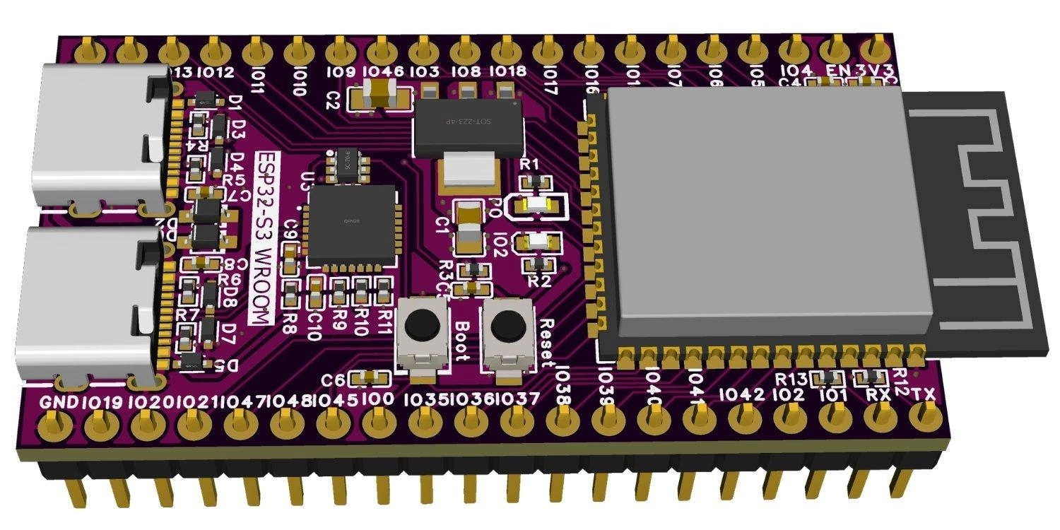
圖:完成的 4-Layer ESP32-S3 Development Board,配置兩組 USB Type-C Connector。
Custom ESP32-S3 Development Board 硬體規格
| 功能 | 規格 |
|---|---|
| MCU | ESP32-S3-WROOM |
| PCB Layers | 4 Layers(Signal - GND - PWR - Signal) |
| Programming Interface | CP2102 USB-to-UART Bridge |
| Native USB Support | USB Type-C OTG Interface |
| Power Input | USB Type-C(Nominal 5 V) |
| Voltage Regulator | AMS1117-3.3 V Low Dropout Regulator(LDO) |
| GPIO Header | 2 × 20 Pins(2.54 mm Pitch) |
| Form Factor | Breadboard Compatible |
Step 1:設計 ESP32-S3 Development Board 原理圖
進入 PCB Layout 之前,首先需要建立完整且可靠的 Schematic。
將 Schematic 拆分成不同 Functional Block,可以簡化 Design Verification,也有助於日後進行 Troubleshooting。
如果之前已經了解過如何設計 ESP32-S2 Module PCB,ESP32-S3 的 Core Circuit 會相對容易理解。不過 ESP32-S3 在 Pin Allocation 與 Dual-Core Architecture 等方面有所不同,因此仍需要仔細進行 Schematic Planning。
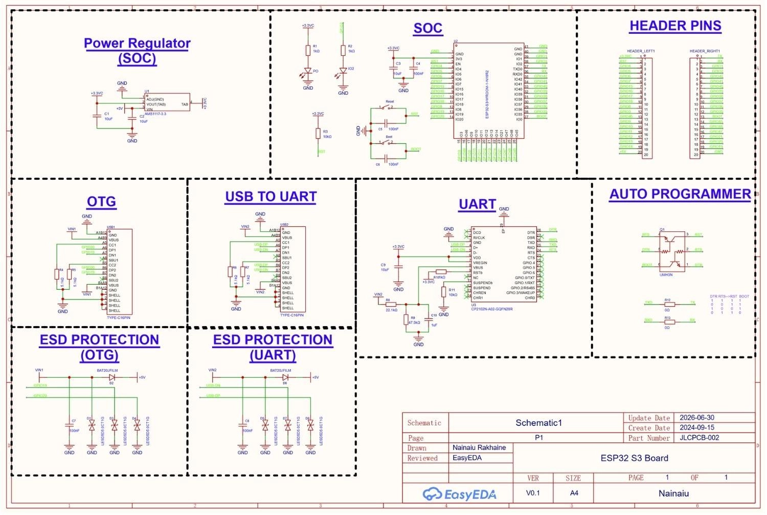
圖:ESP32-S3 Development Board 完整原理圖。
ESP32-S3 Core Circuit
這塊 Development Board 的核心是 ESP32-S3-WROOM Module。
依照 Espressif Hardware Design Guideline,Core Module 配置包括:
- 在 EN(CHIP_PU)Pin 上配置 RC Delay Circuit,以提供穩定的 Startup Delay。
- 在 GPIO0 配置必要的 Pull-Up Resistor,使 Boot Mode Configuration 保持可預測。
- 配置 Tactile Button,讓使用者可以手動執行 Hardware Reset 與 Boot Selection。
ESP32 Power Supply
這塊 Board 由 USB-C Port 的 5 V VBUS 供電。
AMS1117-3.3 Linear Regulator 將 5 V Input 降至 3.3 V System Rail。
為了降低 High-Power Wi-Fi TX Burst 期間出現 Voltage Drop 的風險,本文設計在 Regulator Input 端配置一顆 10 µF Bulk Electrolytic 或 Tantalum Capacitor,並在 3.3 V Output 端搭配一顆 10 µF Ceramic Capacitor。
此外,一顆 Red LED 會透過 Current-Limiting Resistor 連接至 3.3 V Rail,作為 Power Indicator。
USB Programming Interface
為了方便 Firmware Programming 與 Serial Monitoring,本設計加入以 CP2102 為核心的 Dedicated USB-to-UART Bridge。
CP2102 負責 USB-to-Serial Conversion,再將 UART RX/TX 與 ESP32-S3 UART0 連接。
如果需要採購 CP2102、Passive Component、Transistor 與其他 IC,可以透過 JLCPCB Parts Library 查詢相關元件。
Automatic Programmer Circuit
為了避免每次燒錄 Firmware 都必須手動按下 Boot/Reset Button,本設計整合 Automatic Programmer Circuit。
電路使用兩顆一般 NPN Transistor,由 USB-to-UART Bridge 的 DTR 與 RTS Signal 驅動,控制 EN 與 GPIO0 拉低,使 ESP32-S3 自動進入 Bootloader Mode。
Native USB OTG
ESP32-S3 內建 Full-Speed USB OTG Peripheral。
本文將 Native USB Data Line 直接 Routing 到第二組 USB Type-C Connector,並在 CC Pin 使用 5.1 kΩ Pull-Down Resistor。
USB Protection
USB Port 是容易受到 Electrostatic Discharge(ESD)影響的位置,因此本文在 VBUS、D+ 與 D− Pin 後方配置 Low-Capacitance ESD Protection Diode Array,將 Transient Voltage Spike 導向 Ground。
GPIO Header
為了引出 ESP32-S3 的 Functional Pin,本設計使用兩排 20-Pin Male Header。
兩排 Pin Row 的間距為 0.9 inch(22.86 mm),插入 Breadboard 後,Board 兩側各可保留一排 Breadboard Hole。
Status LED
Board 上配置兩顆 LED,方便進行 Visual Debugging:
| LED | 功能 | 配置 |
|---|---|---|
| Power LED | 3.3 V Supply Indicator | 透過 1 kΩ Resistor 連接到 3.3 V Rail。 |
| GPIO2 LED | User-Programmable LED | Active-High LED,連接至 GPIO2,可用於快速執行 Blink Test。 |
表:ESP32-S3 Development Board 上的 Status LED 配置。
Decoupling Capacitor
為了維持穩定的 Power Delivery,Board 上每顆 IC 的 Power Input 都需要搭配適當的 Decoupling Capacitor:
| Capacitor | 用途 | Placement |
|---|---|---|
| 100 nF | Local High-Frequency Decoupling | 緊鄰各個 VCC/3.3 V Pin。 |
| 1 µF | Intermediate Frequency Filtering | 配置在主要 ESP32-S3 VDD Pin 附近。 |
| 10 µF | Bulk Energy Storage | 配置在 LDO Output 與 Main Power Input 附近。 |
| AMS1117 Capacitor | Regulator Stability | 盡可能靠近 Regulator Input/Output Pin。 |
表:ESP32-S3 Development Board 中使用的 Decoupling Capacitor。
Step 2:規劃 ESP32-S3 Development Board 的 4-Layer PCB Stack-Up
Schematic 完成之後,就可以進入 ESP32-S3 PCB Layout 階段。
對 ESP32-S3 這類具有 Wireless Connectivity 與 High-Speed Interface 的 Microcontroller,本文選擇使用 4-Layer PCB Stack-Up。
Internal Plane 可以為 High-Frequency Signal 提供連續 Return Path,有助於降低 Electromagnetic Interference(EMI),同時便於控制 USB Data Line 的 Impedance。
本文使用的 Stack-Up 如下:
| Layer | Type | 功能 |
|---|---|---|
| Top Layer | Signal | Component Footprint、RF Antenna Clearance 與主要 Signal Routing。 |
| Layer 2 | Plane | 完整、不中斷的 Ground(GND)Plane,用於 Shielding 與 Short Return Path。 |
| Layer 3 | Plane | Dedicated 3.3 V Power Plane,用於簡化 Power Distribution。 |
| Bottom Layer | Signal | Secondary Routing、Return-Path Stitching 與 Auxiliary Test Point。 |
表:ESP32-S3 Development Board 的 4-Layer PCB Stack-Up。
Step 3:進行 PCB Component Placement
合理的 Component Placement 是打造乾淨、低 Noise PCB Design 的基礎。
本文將所有 Active 與 Passive Component 都放置在 Top Layer,以簡化 Manufacturing 與 Assembly。
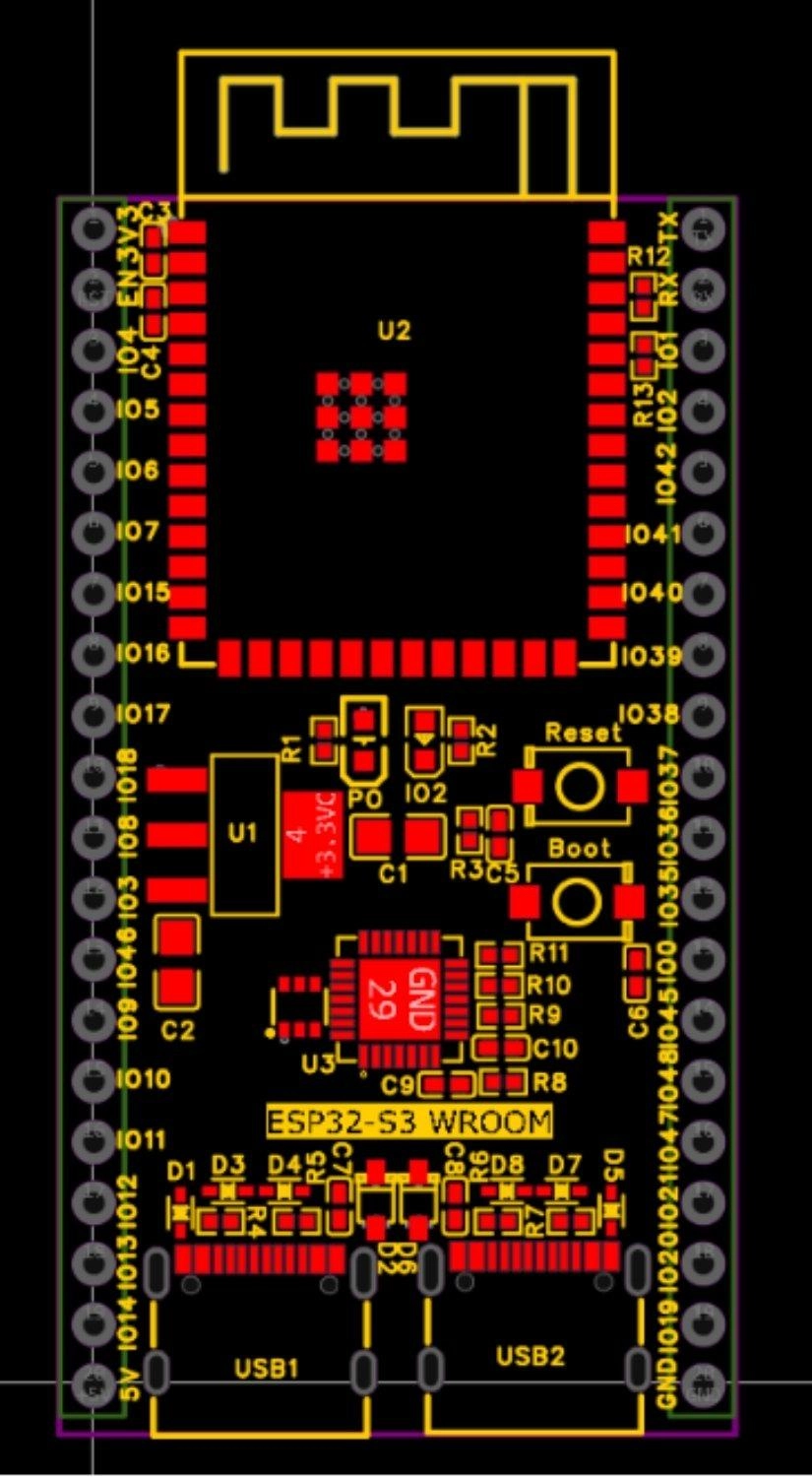
圖:Routing 前的 ESP32-S3 Development Board Component Placement。
主要 Component Placement 規則
-
ESP32-S3 Module: 將 Module 放置在 PCB 的一端。PCB Copper Plane 與 Trace 不應延伸至 Module Onboard PCB Antenna 下方。整個 Antenna Keep-Out Zone 在四個 Layer 上都應保持沒有 Copper,以避免影響 Wireless Signal Range。
-
USB-C Connector: 將兩組 USB Type-C Connector 對齊 PCB Edge。CP2102 應靠近 Programming USB Port,以讓 USB Differential Signal 保持短而直接。
-
Power Circuit: AMS1117 Regulator 與相關 Decoupling Capacitor 應靠近 USB 5 V Input,讓 High-Current Loop 集中在較小區域。
-
Decoupling Capacitor: 每顆 100 nF Bypass Capacitor 應直接靠近對應 Power Pin。本文的 Routing 方式是讓 Power Connection 經過 Capacitor Pad 附近後再進入 IC Pin,並在 Capacitor Ground Pad 旁配置 Ground Via,以縮短 Return Current Path。
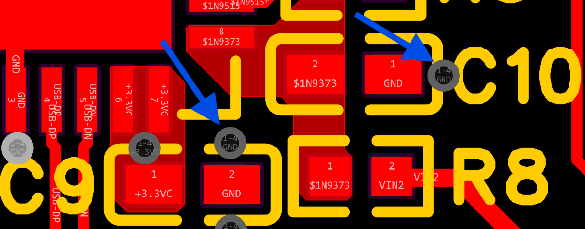
圖:將 Decoupling Capacitor 靠近 Target IC,並在 Capacitor Ground Pad 旁配置 Ground Via,以縮短 Return Current Path。
Step 4:Routing ESP32-S3 PCB
PCB Routing 會把 Schematic 中的 Electrical Connection 轉換成實際 Copper Trace。
本文需要特別注意 Differential Pair 與 Power Routing。
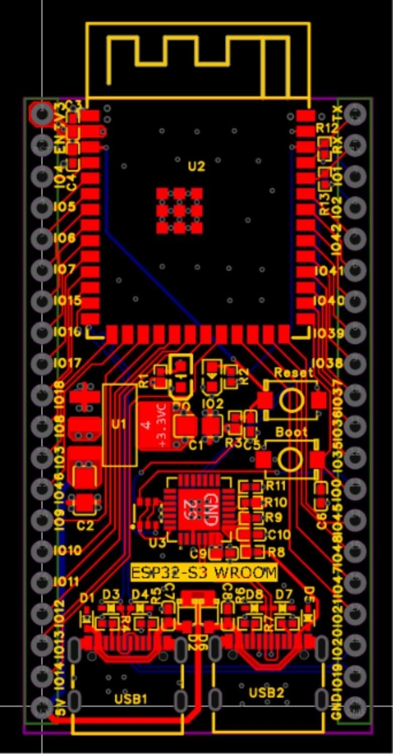
圖:完成 Signal Trace 與 Power Routing 的 ESP32-S3 PCB。
1. 優先 Routing Critical Signal
首先 Routing USB Differential Pair,再處理其他 Signal。
可以使用 JLCPCB PCB Impedance Calculator,根據實際 PCB Stack-Up 計算需要的 Trace Width 與 Spacing。
在本文設計所使用的 Stack-Up 中,6 mil Trace Width 與 10 mil Gap 用於達到目標 90 Ω Differential Impedance。
D+ 與 D− Trace 應:
- 保持 Parallel Routing
- 盡量維持相近 Length
- 在可能的情況下避免不必要 Via
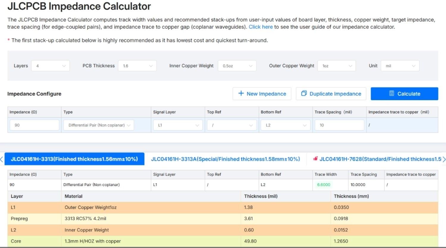
圖:JLCPCB PCB Impedance Calculator,本文範例設定 6 mil Trace、10 mil Gap,以取得 90 Ω USB Differential Pair。
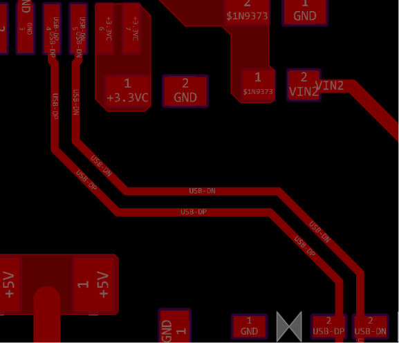
圖:90 Ω USB Differential Pair Routing。
Differential Pair 應盡量維持 Equal Length。如果長度不同,可以透過 PCB Design Software 進行 Length Tuning。
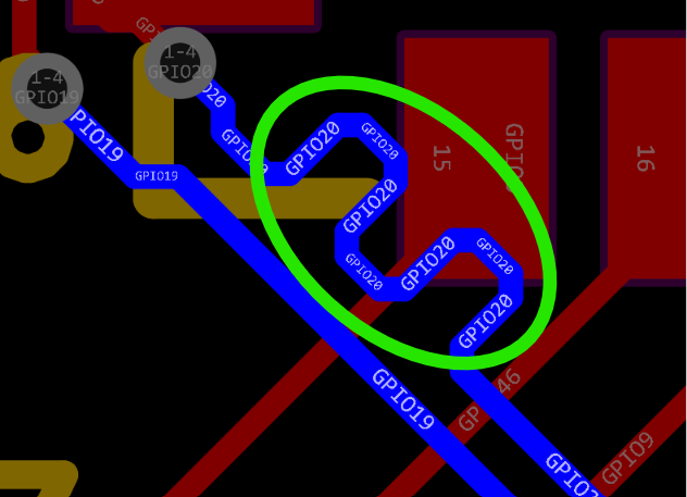
圖:透過 Equal-Length Tuning 讓 Differential Pair Trace Length 相匹配。
2. 連接 Power 與 Ground Plane
與其在整塊 PCB 上使用細長的 3.3 V Trace,本設計透過 Via 直接連接至 Layer 3 Power Plane。
Ground Connection 則直接透過 Via 連接 Layer 2 Ground Plane。
這種 Low-Impedance Connection 可以降低 Connection 中的 Parasitic Effect。
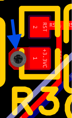
圖:3.3 V Via 與 Trace 連接 Power Plane。
3. 依 Current-Carrying Capacity 設定 PCB Trace Width
本文設計中的一般 Signal Trace Width 約為 6–8 mil。
Power Line 則使用較寬的 Trace,原文設定為至少約 15–25 mil,或直接使用 Dedicated Polygon Pour,以處理 Wireless Transmission 期間最高約 500 mA 的 Current Demand。
Step 5:加入 Ground Copper Pour 與 Via Stitching
Routing 完成後,在 Top 與 Bottom Signal Layer 加入 Solid Ground Copper Pour。
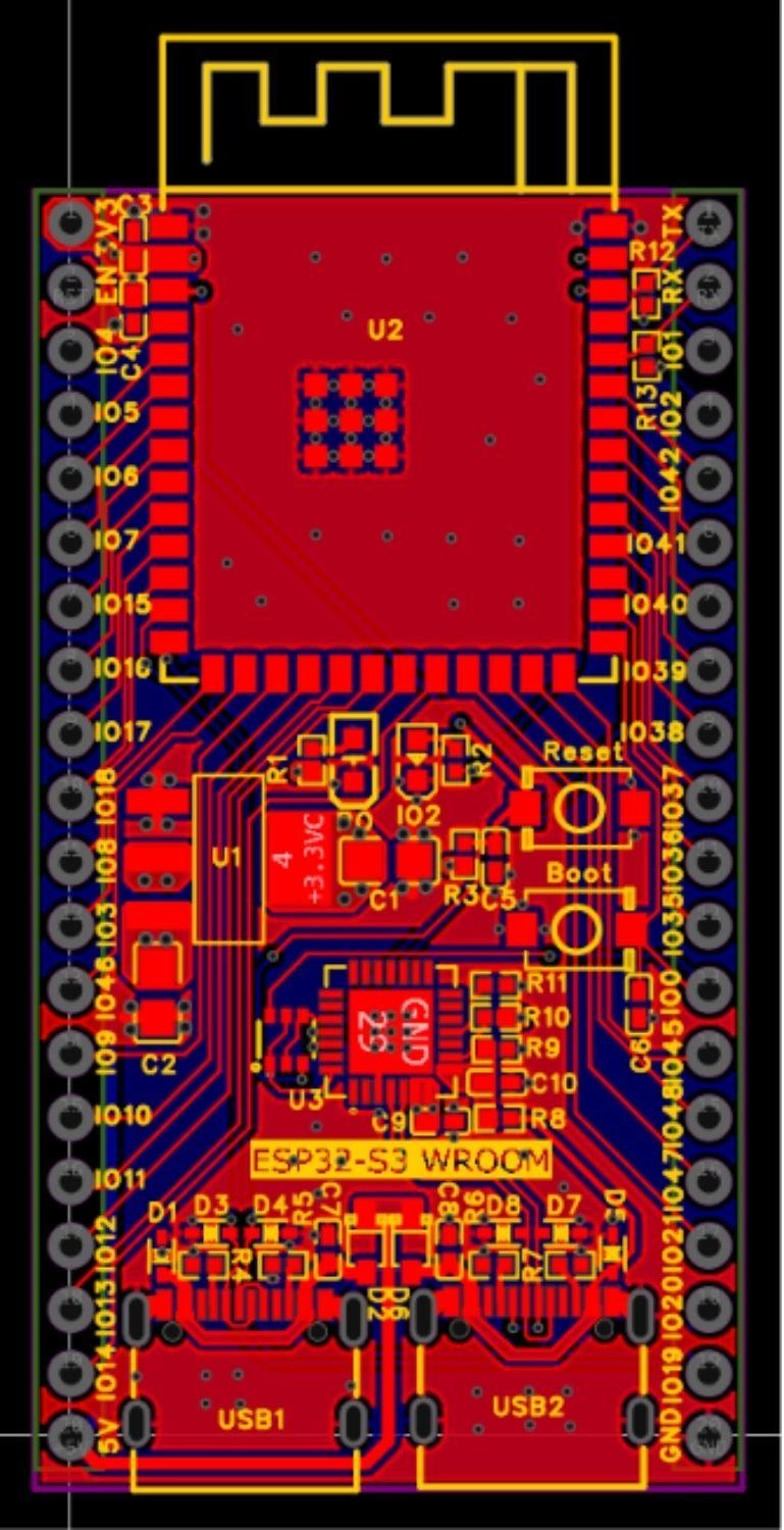
圖:完成 Ground Copper Pour 與 Ground Stitching Via 的 ESP32-S3 PCB。
這些 Ground Copper Pour 可以作為 Shielding 的一部分。
為了讓不同 Ground Region 彼此連接,本設計進一步加入 Via Stitching。
原文設計在 PCB Perimeter 周圍約每 2–3 mm 配置 Ground Via,以形成類似 Via Fence/Faraday Cage 的結構,降低 EMI。
Step 6:進行最終 PCB Check 與 Design Rule Check(DRC)
輸出 Fabrication File 之前,應完成以下 Visual 與 Automated Check:
- Silkscreen Cleanup: 在 Top Silkscreen 上清楚標示所有 GPIO Pin。標記 Reset(RST)與 Boot(BOOT)Button,並加入 Status LED 的 Polarity Mark。
- Design Rule Check(DRC): 依 PCB Manufacturer 提供的實際 Clearance、Minimum Trace Width 與 Drill Hole Constraint 設定 PCB Design Software DRC,確認設計位於允許的 Fabrication Tolerance 內。
Step 7:產生 ESP32-S3 PCB Manufacturing File
PCB Layout 通過 DRC 後,就可以輸出 Production 所需的檔案。
標準 PCB Fabrication 通常需要:
- Gerber Files
- Excellon Drill Files
如果希望使用 Automated Assembly Service,還需要:
- Bill of Materials(BOM): 列出 Part Number、Reference Designator 與 Package 等 Component Information 的表格。
- CPL/Centroid File: 包含每顆 Component 的 X-Y Coordinate 與 Rotation Angle。
正式輸出前,應再次確認 Component Footprint 與 BOM 中指定的實際 Component Package 完全一致。
Step 8:透過 JLCPCB 製作 ESP32-S3 Development Board
完成所有檔案後,即可進入 PCB Ordering Process:
-
前往 JLCPCB 報價頁面,上傳已壓縮的 Gerber ZIP File。
-
Online Gerber Viewer 會解析檔案,並顯示 PCB Layer、Drill Hole 與 Board Dimension 的 Visual Preview。
-
設定實際 PCB Manufacturing Parameter,例如 Layer Count、PCB Thickness、Solder Mask 與 Surface Finish。
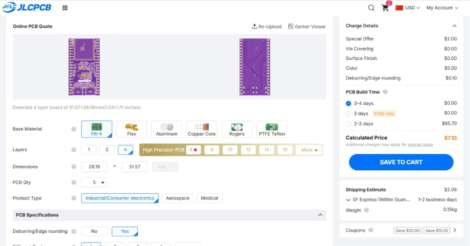
圖:將 Gerber Files 上傳至 JLCPCB 進行 PCB Fabrication。
原文對一般 Prototype Run 列出的標準設定包括:
- PCB Thickness: 1.6 mm,或需要稍薄 Profile 時使用 1.2 mm。
- Solder Mask Color: Green、Blue、Black、Red 或 Yellow。
- Surface Finish: 基礎 Prototype 可選 HASL(含鉛),或使用 ENIG(Electroless Nickel Immersion Gold,化學鎳金)取得更平坦的 Pad 與良好 Solderability。
Step 9:組裝 ESP32-S3 Development Board
相較手工焊接 CP2102 與 USB-C Connector 等 Fine-Pitch Component,也可以使用 JLCPCB PCB Assembly,並上傳前面產生的 BOM 與 Pick and Place(CPL)File。
在 Automated SMT Assembly Process 中,工廠會先透過 Precision Stencil 印刷 Solder Paste,再利用 Pick-and-Place Machine 放置 Component,最後經過 Multi-Zone Reflow Soldering 完成焊接。
ESP32-S3 Development Board PCB 製造流程
| Step | 操作 | 主要輸出/結果 |
|---|---|---|
| 1 | Schematic Design | 定義 Circuit、ESP32 Connection 與 ESD Protection。 |
| 2 | PCB Layout & Routing | 配置 Component、Routing 90 Ω USB Differential Pair,並執行 DRC。 |
| 3 | Manufacturing Export | 產生 Gerber、NC Drill、BOM 與 Pick & Place(CPL)File。 |
| 4 | Quote & Upload | 將 Gerber 上傳至 JLCPCB Quote Page。 |
| 5 | Parameter Selection | 選擇 Layer Count、Board Thickness 與 Solder Mask Color。 |
| 6 | PCBA Setup(Optional) | 上傳 BOM/CPL File,設定 Automated SMT Assembly。 |
| 7 | Production & Quality | Stencil Printing、Automated Placement、Reflow Soldering 與 AOI Inspection。 |
| 8 | Delivery | 完成製造與組裝的 Development Board 交付。 |
表:從 ESP32-S3 PCB Design 到透過 JLCPCB 完成 Manufacturing 的完整流程。
結論
自行設計 Custom ESP32-S3 Development Board,是從 Development Module 進一步邁向完整 Hardware Design 的重要一步。
從簡單的 2-Layer Layout 轉向較完整的 4-Layer Architecture,可以利用 Dedicated Ground/Power Plane 改善 Power Distribution、Return Path 與 High-Speed Signal Routing。
透過本文的完整 Design Workflow——從 Schematic Functional Block、Component Placement、適當 Trace Width、Differential Pair Routing,到最終 Design Rule Verification——可以降低 Board Respin 與 Hardware Bug 的風險。
完成 Gerber、BOM 與 CPL 後,再搭配 Automated Assembly Service,就可以把螢幕上的 ESP32-S3 Design 進一步轉換為真正完成製造與組裝的 Development Board。
ESP32-S3 PCB Design 常見問題
問:為什麼 ESP32-S3 通常更適合使用 4-Layer PCB,而不是 2-Layer PCB?
ESP32-S3 是整合 Wi-Fi 與 Bluetooth 的 High-Frequency System-on-Chip。4-Layer PCB 可以在 Signal Layer 附近配置 Dedicated Ground 與 Power Plane,協助降低 EMI、縮小 Current Loop Inductance,並改善 USB 等 High-Speed Trace 的 Impedance Control。
問:USB-C Data Trace 是否需要進行精確的 Impedance Routing?
需要。ESP32-S3 Native USB 與 CP2102 USB Data Line 都使用 Differential Signaling。為了降低 Signal Reflection 與 Data Integrity 問題,本文按照 USB Differential Pair 的 90 Ω Target Differential Impedance 進行 Routing。
實際 Trace Width 與 Spacing 必須根據 PCB Manufacturer 提供的 Stack-Up、Dielectric Thickness 與 Copper Thickness 計算。
問:為什麼 ESP32-S3 Module 的 Antenna 下方需要 Keep-Out Area?
ESP32-S3-WROOM Module 使用 Onboard PCB Antenna。Antenna 下方或附近的 Copper Plane、Trace 與 Component 可能對 RF Field 造成 Shielding 或 Detuning,進而降低 Wi-Fi 與 Bluetooth Wireless Range。
因此 PCB Layout 應按照 Module Hardware Design Guideline 保留指定 Antenna Keep-Out Area。
問:下單之前要如何確認 Custom PCB Footprint 是否正確?
應將 PCB Footprint 與 Component Manufacturer Datasheet 中的 Package Dimension、Recommended Land Pattern 與 Pin Definition 逐一核對。
另外,也可以使用 PCB CAD Software 的 3D Viewer,或匯出 STEP 3D Model,檢查 Connector、Module 與其他 Component 的 Physical Size、Orientation 與 Mechanical Alignment,再提交 Manufacturing File。
持續學習
如何讀取電阻色碼:附色碼表與實例的完整指南
四環電阻色碼解析 四環電阻色碼是電子元件標示阻值最常見的方法之一。這種標示方式廣泛用於協助工程師與電子愛好者快速判讀阻值,無需使用電阻色碼計算器。 標準四環電阻的各個色環代表以下意義: 第一環(數字 1):代表第一位有效數字。 第二環(數字 2):代表第二位有效數字。 第三環(倍率):表示前兩位數字需要乘上的倍率。 第四環(公差):表示實際阻值相對於標稱阻值的容許偏差。 如何讀取四環電阻色碼 準備工作:拿起電阻,將與其他色環間距最大的一環(或金色/銀色色環)放在右側,然後由左向右讀取。 第一環與第二環(數字):將顏色與色碼表對照,找出前兩位數字。 第三環(倍率):表示需要在前兩位數字後面加上多少個零。 第四環(公差):表示電阻的精確度,例如金色代表 ±5%。 範例:1 kΩ 電阻(四環) 這是最常用的電阻之一,經常出現在上拉電路及基本 LED 應用中。 第一環:棕色(1) 第二環:黑色(0) 倍率:紅色(×100) 公差:金色(±5%) 計算方式: 10 × 100 = 1,000 Ω(1 kΩ) 五環電阻色碼解析 五環電阻色碼通常用於高精度電阻。與四環電阻色碼相比,五環版本透過增加一位有效數字,......
如何從零開始設計 ESP32-S3 開發板:4 層 PCB 設計教學
自行設計 ESP32-S3 Development Board,可以讓您完整掌控 Hardware Architecture,同時為 IoT Project 後續進入 Commercial Production 做好準備。 相較直接使用體積較大的 Off-the-Shelf Development Board,Custom Design 可以讓您: 最佳化 PCB Board Space 只引出實際需要的 GPIO 將 Peripheral 直接整合到同一塊 PCB 依實際產品需求規劃 Power、USB、Protection 與 Connector 本教學將從零開始設計一塊 4-Layer ESP32-S3 Development Board。 我們將完整介紹 Hardware Development Pipeline,包括 ESP32-S3 Schematic 架構、4-Layer PCB Stack-Up 規劃、PCB Routing Best Practices,以及如何準備可直接用於 JLCPCB PCB Fabrication 與 Assembly 的製造檔案。 完成後的 Develo......
IC Symbol 完整指南:積體電路符號、Pin Mapping、Circuit Diagram 與 PCB 應用
可以把積體電路(Integrated Circuit,IC)想像成一座微型的電子城市。 工程師不需要在 Schematic 中逐一畫出數百、數千,甚至更多內部電子元件,而是利用一個清楚的 Integrated Circuit Symbol(積體電路符號/IC 符號),代表整個功能系統。 實體 IC 可能只是一顆帶有金屬接腳的小型黑色晶片,但在電路原理圖中,IC Schematic Symbol 更像是一張功能地圖。 只要能正確理解這些 Electronic IC Symbol,就能更有效率地進行 Circuit Design、PCB Design 與 Troubleshooting。 本指南將介紹: 了解 Integrated Circuit Symbol 在 Circuit Diagram 中的意義 辨識不同類型的 IC Symbol 了解 IC Pin 與功能如何在符號中表示 逐步學習如何判讀 IC Symbol 查看 IC 在實際 Circuit Diagram 中的應用 了解如何從 Schematic Symbol 轉換至 PCB Design 圖:從不同 Integrated Circu......
Transformer Symbol 完整指南:類型、Dot Convention 與 PCB 應用
變壓器(Transformer)是電力電子中的基礎元件,廣泛用於電壓轉換、電氣隔離、阻抗匹配與訊號耦合。 因此,變壓器符號(Transformer Symbol)廣泛出現在電源轉接器、SMPS、音訊系統、通訊介面與工業電子設備的電路原理圖中。 如果您曾經把變壓器符號與電感器符號混淆,或一直不明白繞組旁的小圓點代表什麼,本指南將完整說明變壓器符號的判讀方式。 本文將介紹: Transformer Symbol 的結構與圖示 Dot Convention 與繞組極性 升壓與降壓變壓器符號 隔離、中心抽頭與自耦變壓器符號 如何在電路圖中判讀變壓器 Transformer vs. Inductor Symbol 變壓器在電源轉接器與 SMPS 中的應用 Transformer Symbol 與 PCB Layout 的關係 常見 Transformer Symbol 使用錯誤 圖:電路原理圖中的變壓器符號,以及實際安裝在 PCB 上的變壓器元件。 什麼是 Transformer Symbol? Transformer Symbol 是在電路原理圖中,用來表示變壓器元件的標準化圖形符號。 透過符號可以表達:......
接地符號完整指南:Earth、Chassis、Signal、AGND、DGND 與 PGND
重點摘要 ⬇ 下載接地符號速查表(PDF) 將六種常見接地符號及其標準編號整理在同一頁,方便快速查閱。 四種 IEC 60417 符號:IEC 60417 定義 5017 為大地接地、5018 為功能接地、5019 為保護接地,以及 5020 為機架/機殼。 保護接地與安全直接相關:IEC 60417-5019 用於識別保護接地連接,適用於與電氣安全相關的保護性等電位連接。 訊號接地採用不同慣例:IEEE Std 315 定義訊號接地符號,以及用於電路參考點的不同標示形式。 機殼不一定等於大地:Chassis/Frame 可能處於與大地不同的電位,因此不能自動假設機殼接地就是 Earth Connection。 接地符號可能是任何原理圖中最常見的符號之一,因此很容易讓人以為所有 Ground Symbol 都代表相同意思。但實際上並不是這樣。 Earth、Protective Earth、Chassis 與 Signal Ground 各自具有不同用途。混淆這些接地類型,可能造成 Ground Loop、電位偏移與 EMI 等訊號完整性問題,嚴重時甚至可能因設備外殼沒有正確保護接地而形成安全風險。......
IGBT 符號完整指南:G/C/E 接腳、N/P 通道、續流二極體與判讀
重點摘要 先辨識端子:閘極(G)、集極(C)與射極(E)是 IGBT 的三個主要端子。 了解不同符號形式:可以並列比較 N 通道與 P 通道 IGBT 符號,理解兩者不同的箭頭表示方式。 不要只依賴單一繪圖樣式:IEC 與 ANSI/IEEE 的 IGBT 符號外觀可能不同,即使它們代表的是同一類元件。 另外確認二極體:反並聯續流二極體可能直接包含在 IGBT 符號中,也可能以獨立元件表示,取決於繪圖慣例與實際應用。 連接 Gate Driver 前務必確認:應以製造商 Datasheet 的 Pinout 為準,不要假設原理圖符號與實體封裝 Pin 順序完全相同。 IGBT 符號乍看之下與功率 MOSFET 符號非常相似,因此第一次看到時很容易把兩者混淆。 在馬達功率轉換器中,如果誤將 IGBT 判斷成 MOSFET,就可能造成錯誤的 Gate Driver 連接方式,甚至接錯元件的主要功率端子。 此外,IEC、ANSI、Datasheet 與不同 EDA 元件庫所使用的符號形式也可能有所差異,使 IGBT 的辨識變得更加複雜。 在本指南中,您將了解: 並列比較 N 通道與 P 通道 IGBT ......