電路板接地平面與電源平面指南 2026
12 分鐘
- Ground Plane PCB 設計:核心原則
- PCB Power Plane 設計:Layout 最佳實務
- High-Speed 与 Mixed-Signal PCB 的 Ground Plane 设计
- 常见 PCB Power Plane 错误与解决方法
- Circuit Board Ground Plane 常见问题
- Circuit Board Ground Plane 结论
重點摘要
優先保持銅箔連續:完整的 PCB Ground Plane(接地平面)可以建立 Low-Impedance Return Path、降低 Noise,而且即使在 Mixed-Signal PCB 中,通常也比任意分割 Ground Plane 更安全。
從 Current Loop 思考:每一條 Signal 都需要完整的 Return Path。High-Speed Trace 不應跨越 Plane Gap、Slot 或 Cutout。
提早規劃 Stack-Up:在 Routing Critical Signal 之前先決定 Layer Arrangement,並盡量讓 Power Plane 與 Ground Plane 靠近,以降低 Power Distribution Path 的 Inductance。
Placement 比事後補 Filter 更重要:縮短 Decoupling Loop、合理配置 Stitching Via,以及妥善進行 Component Grouping,可以從 Layout 階段降低大量 EMI 與 Ground Loop 問題。
製造前再次驗證:重新計算 Copper Pour、執行 DRC、檢查 Gerber,並確認 Stack-Up 與 Copper Weight 符合 PCB Manufacturer 的實際製造能力。
設計良好的 Circuit Board Ground Plane,不只是提供一個方便的 Ground Connection。
它可以建立 Low-Impedance Return Path、降低 PCB 不同位置之間不必要的 Voltage Difference,並協助控制 High-Speed Signal 與 Switching Circuit 所產生的 Noise。
同樣的原則也適用於 PCB Layout 中的 Power Plane(電源平面)。穩定的 Current Delivery 與較低的 Power Distribution Impedance,都會直接影響 Circuit Reliability。
如果 Ground/Power Plane 規劃不良,可能造成:
- 過長的 Return Path
- Ground Loop
- Voltage Drop
- Electromagnetic Interference(EMI)
- Signal Integrity 問題
當 PCB 包含 Fast Digital Interface、Sensitive Analog Circuit、Switching Regulator 或多組 Voltage Rail 時,這些問題會更加明顯。
Ground 與 Power Copper 同時也會影響 Thermal Management,可以協助將 High-Current Component 產生的熱量分散至較大的 Copper Area,降低局部 Hotspot。
本文將介紹實際 PCB Ground Plane Design,包括 Return Path Planning、Via Stitching、Layer Stack-Up Selection、Decoupling Capacitor Placement,以及 Multi-Voltage Power Plane Segmentation。
如果 PCB Routing 較密集或結構複雜,也可以使用 JLCPCB Layout Service,依照完成的 Schematic 協助 Component Placement、Routing 與考慮製造能力的 PCB Layout。
Ground Plane PCB 設計:核心原則
PCB Layout 中常見的一個錯誤,是把 Ground Plane 當成 Routing 完成之後再補上的 Copper Area。
實際上,Ground Plane 應該從設計初期就直接影響 Component Placement 與 Signal Routing。
一條 Trace 在 Signal Layer 上看起來可能非常合理,但它下方的 Return Current 卻可能被迫繞行很長的路徑。
這種看不見的 Return Path,往往才是 Noise、Ringing 或意外 EMI 問題真正的來源。
良好的 Ground Plane PCB Design,首先需要決定哪一個 Copper Layer 將作為 Critical Signal 的主要 Reference Plane。
High-Speed Trace 應盡量保持在連續 Copper Plane 上方,不要跨越:
- Plane Gap
- Slot
- Cutout
- Disconnected Copper Region
當 Reference Plane 被中斷時,Return Current 無法繼續沿著 Signal Trace 下方流動,而必須繞過 Opening。
這會增加 Current Loop Area,同時提高 Return Path Inductance。
Routing 完成後,也需要重新檢查 Ground Plane。
Pad、Via 與 Board Edge 周圍的 Clearance,可能在 Copper Pour 中形成:
- Narrow Copper Neck
- Isolated Copper Island
- 意外的 Plane Discontinuity
這些問題不一定會直接觸發 Design Rule Error,但仍可能影響 Current Flow 與 Noise Performance。
Plane Design 快速檢查清單
第一次完成 Routing Review 前,可以按照以下項目進行檢查:
- 在 Layout 允許的情況下,讓主要 Ground Region 保持盡可能連續。
- 檢查每一條 High-Speed Trace 與 Clock Trace 下方實際是什麼 Copper Reference。
- 不要讓 Critical Signal 跨越 Plane Gap 或 Cutout。
- 將 Decoupling Capacitor 靠近對應 IC Power Pin。
- Signal Change Layer 時,在需要的位置提供附近的 Ground/Return Transition Via。
- 檢查狹窄 Copper Neck 與 Isolated Copper Island。
- 每次進行重大 Layout Modification 後,重新計算 Copper Area 並執行 DRC。
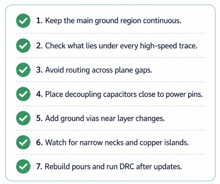
Ground Plane PCB Design 快速檢查清單。
Solid Ground Plane vs. Split Ground Plane
對大多數 PCB Layout 而言,Solid Ground Plane(完整接地平面)通常是比較安全的起點。
它可以為 Signal Return Current 提供連續路徑,降低 Return Current 因 Gap 或 Narrow Copper Section 而被迫繞行的可能性。
這對以下 Fast Signal 尤其重要:
- Clock
- Communication Line
- High-Speed Digital Signal
因為 Frequency 越高,Return Current 越傾向集中在 Signal Trace 附近的 Reference Plane 上。
Split Ground Plane(分割接地平面)則會把 Ground Copper 分成不同區域。
部分 Designer 會使用這種方式,希望把 Noisy Switching Circuit 與 Sensitive Analog Section 隔離。
真正的問題通常發生在 Signal Trace 跨越兩個 Ground Region 之間的 Gap 時。
Signal Trace 本身可以直接跨過 Gap,但 Return Current 無法穿越不存在的 Copper,只能繞過 Split。
結果會造成:
- Current Loop Area 增加
- Return Path Inductance 增加
- Noise 增加
- EMI Risk 提升
因此,在 Mixed-Signal PCB 中,不應把「分割 Ground Plane」當成自動套用的標準答案。
很多情況下,一個 Continuous Ground Plane 搭配合理的 Component Placement,反而會得到更好的結果。
可以把:
- Switching Converter
- Digital Processor
- Sensitive Analog Circuit
在實體 Placement 上分區,再控制不同 Current Path 在 Plane 上的流向。
如果 System 確實需要 Split Ground,則不要讓 Critical Signal 任意跨越 Split。
同時應查看 Component Manufacturer 的 Grounding Recommendation,確認不同 Ground Region 應如何連接。
Ground Plane Design 真正需要考慮的是完整 Current Path,而不只是 Copper Shape。
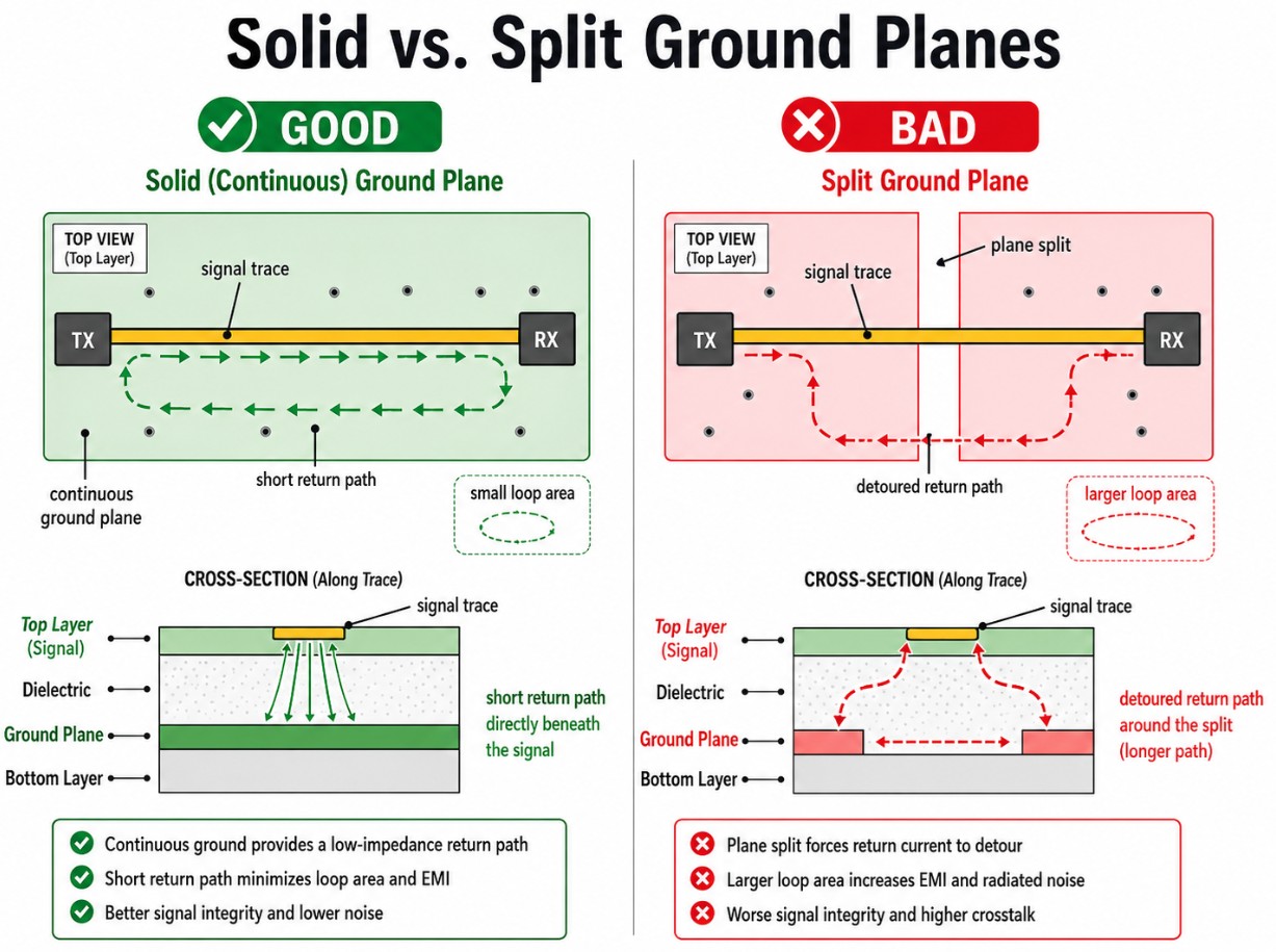
Solid Ground Plane 與 Split Ground Plane 的 Return Path 比較。
Return Path 規劃
Signal Trace 只代表 Current Path 的一半。
電流從 Driver 流向 Receiver 後,還必須回到 Source,而這個 Return Path 通常會經過最近的 Ground Reference。
這條第二路徑很容易被忽略,因為它不像 Signal Trace 一樣直接畫在 Signal Layer 上。
在規劃良好的 PCB 中,Return Current 可以在 Signal Trace 下方的 Ground Plane 中流動。
Outgoing Current 與 Return Current 彼此靠近,因此可以維持較小的 Current Loop Area。
當 Signal Trace 跨越:
- Slot
- Plane Boundary
- Isolated Copper Region
時,就會出現問題。
Signal 可以直接跨越 Opening,但 Return Current 必須繞過它。
因此,一條在 PCB Editor 中看起來很短的 Trace,實際上可能形成非常大的 Current Loop。
Connector 與 Signal Via 附近尤其值得注意。
當 Signal Change Layer 時,它所參考的 Plane 也可能發生變化。
如果上下 Reference 都是 Ground,將 Ground Stitching Via 放在 Signal Via 附近,可以為 Return Current 提供較短的 Layer Transition Path。
如果 Reference Plane 類型發生改變,例如從 Ground Reference 轉換到 Power Reference,則應依實際 Stack-Up 與 Signal Frequency 規劃相應的 Return Transition,而不能只看 Signal Via 本身。
Layout Review 時,應特別檢查:
- Clock Line
- USB Signal
- Communication Bus
- Fast Digital Interface
- Switching Node
下方的 Copper Reference。
不要只從 Driver 到 Receiver 看 Signal Trace,而要追蹤完整的:
Driver → Signal → Receiver → Return Path → Source
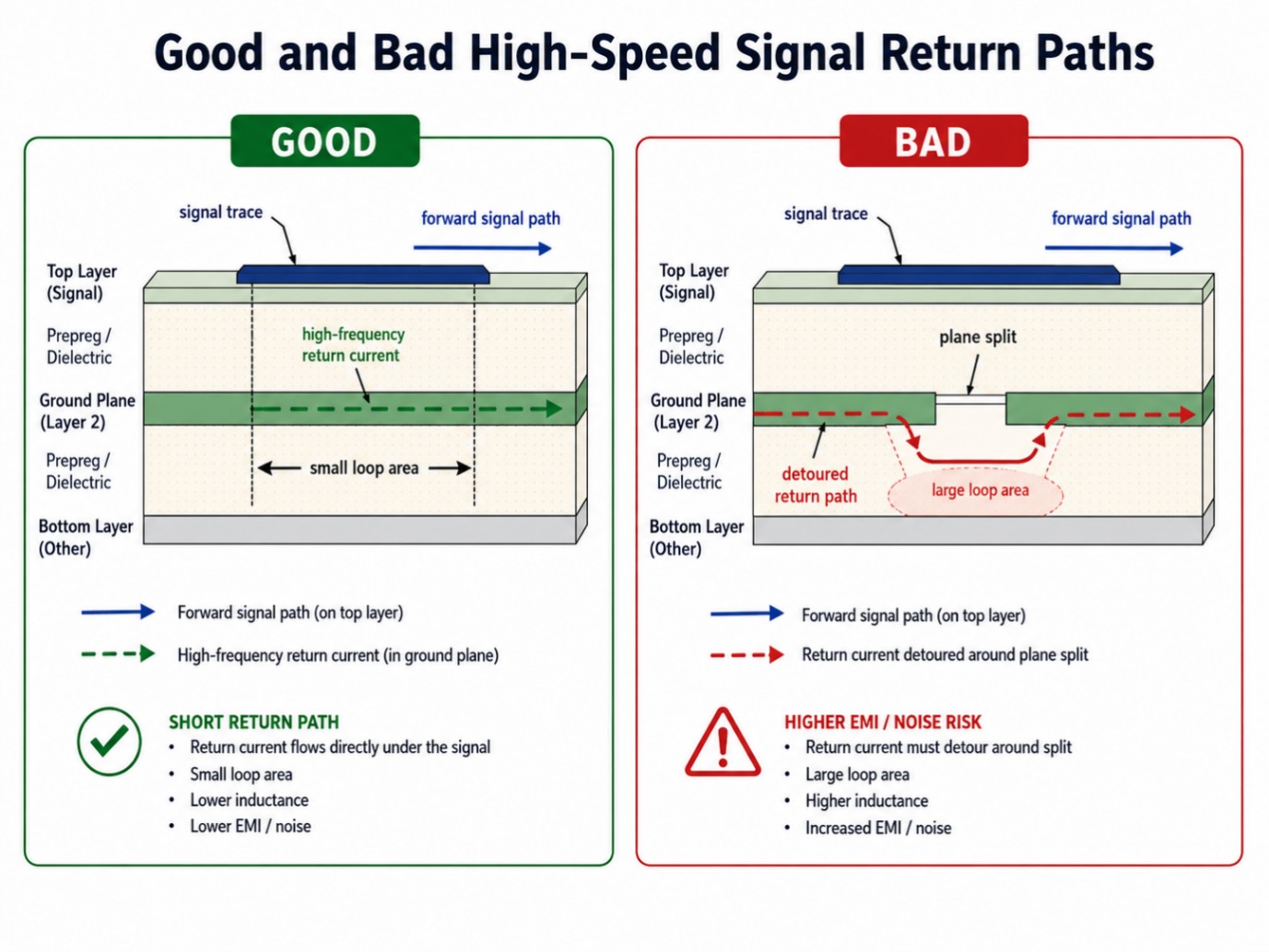
High-Speed Signal 良好與不良 Return Path 的比較。
Texas Instruments High-Speed Layout Guidelines 也指出,Reference Plane 中的 Slot 會迫使 Return Current 改變路徑,進而增加 Current Loop Area。
Via Stitching 策略
Ground Stitching Via(接地縫合過孔)只有在具有明確 Electrical Purpose 時才能發揮最大作用。
在 PCB 所有空白位置放滿 Via,看起來可能很完整,但對實際效果而言,位置通常比單純的數量更加重要。
可以優先檢查以下位置:
- Signal Layer Transition
- Board Edge
- Noisy Circuit Boundary
- Sensitive Circuit Boundary
- RF Area
- Shield Region
當 High-Speed Signal Change Layer 時,如果兩個 Signal Layer 都參考 Ground Plane,Signal Via 附近的 Ground Via 可以讓 Return Current 快速在不同 Ground Layer 之間轉移。
如果 Stitching Via 距離過遠,Return Current 必須先在 PCB 上繞行,再回到 Signal 附近。
這會增加 Path Inductance,也可能提高 Noise。
Via Stitching 同樣常見於:
- PCB Edge
- RF Section
- Switching Converter
- Shielded Area
一排 Grounded Via 可以把多層 Ground Copper 連接在一起,降低 PCB Edge 成為意外 Radiation Source 的可能性。
同樣的技術也可以協助限制 Fast Switching Loop 周圍的 Current Distribution。
但 Via Stitching 無法彌補:
- 不合理的 Component Placement
- 破碎的 Ground Plane
- 過大的 Switching Loop
加入 Via 後,也要重新檢查 Copper Pour。
Pad 與 Trace 周圍的 Clearance 可能形成不容易在正常 Zoom 下發現的狹窄 Copper Section。
因此應重新 Build Copper Pour、檢查 Connection,並執行 DRC。
EasyEDA PCB Tools 也提供在相同 Net 的重疊 Copper Region 之間新增或移除 Via 的相關工具。
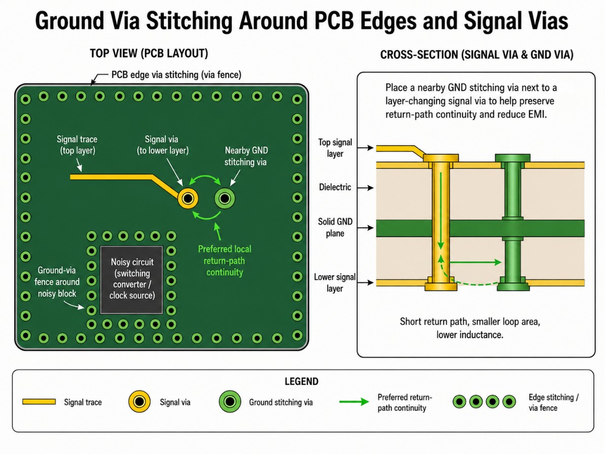
PCB Edge 與 Signal Via 周圍的 Ground Via Stitching。
PCB Power Plane 設計:Layout 最佳實務
Power Plane 看起來可能只是一大片 Copper Area,但它的 Geometry 會直接影響:
- Voltage Stability
- Heat Distribution
- Noise
- Current-Carrying Capability
一個 Connection 在 Schematic 上可能完全正確,但在實際 PCB 上仍可能表現不佳。
常見原因包括 Supply Current 被迫流經:
- Narrow Copper Neck
- Long Current Path
- 數量不足或尺寸不合適的 Via
良好的 Power Plane 應該從 Power Source 到每個 Load 提供短而合理寬度的 Current Path。
需要特別檢查:
- Power Connector
- Regulator Output
- Large Capacitor
- Mounting Hole
- Dense Component Area
Pad 與 Trace Clearance 有時會移除比預期更多的 Copper,使大型 Power Region 中只剩下一條狹窄的 Connection。
Power Plane 也必須和 Ground Plane 一起考慮。
當 Power 與 Ground Layer 彼此靠近時,可以降低 Power Distribution Path 的 Inductance,並形成一定程度的 Distributed Capacitance。
這有助於 Decoupling Network 在 IC 突然需要 Current 時維持較低 Impedance。
最終 Geometry 仍會受到以下因素影響:
- Copper Thickness
- Board Thickness
- Dielectric Spacing
- Current Level
- Manufacturing Stack-Up
完成設計前,可以參考 JLCPCB Multi-Layer PCB Standard Laminated Structures,確認實際可用的 Layer Construction。
Controlled-Impedance Trace 則可以透過 JLCPCB PCB Impedance Calculator,按照實際 Stack-Up 計算,而不是直接套用通用 Layer Parameter。
Layer Stack-Up Arrangement
在 Routing Clock、Communication Bus 或 Controlled-Impedance Trace 之前,就應先確定 PCB Stack-Up。
如果在 Project 後期才改變 Layer Order,可能會:
- 改變 Trace Impedance
- 改變 Reference Plane
- 造成原本 Critical Signal 參考到錯誤的 Copper Layer
一種常見的 4-Layer PCB 配置範例是:
- Top Layer — Component + Signal Routing
- Inner Layer 1 — Continuous Ground Plane
- Inner Layer 2 — Power Region + Slower Signal
- Bottom Layer — Signal Routing
這種配置可以讓 Top-Layer Signal 擁有非常接近的 Ground Reference。
同時也能提供 Internal Layer 給主要 Power Rail 使用。
但如果 Inner Layer 2 被分成多個 Voltage Region,就要特別檢查 Bottom-Layer Fast Signal 是否跨越 Power Region 之間的 Gap。
6-Layer PCB 可以提供更多 Reference Plane 選擇。
一種可能的配置是:
- Top Signal
- Ground Plane
- Internal Signal
- Power Plane
- Ground Plane
- Bottom Signal
第二個 Ground Layer 可以為 Bottom-Layer Routing 提供更近的 Reference,並讓部分 Signal Transition 更容易維持 Return Path。
不过,这只是一个示例,并不是所有 6-Layer PCB 的固定最佳结构。
以下 Design 可能需要不同 Stack-Up:
- Dense BGA Routing
- RF Circuit
- Fast Memory Interface
- High-Current Power Section
最终 Stack-Up 必须符合 PCB Manufacturer 的实际制造能力。
Dielectric Thickness 与 Copper Weight 都会影响 Impedance,因此在确认 Manufacturer Stack-Up 前,不应最终锁定 Controlled-Impedance Trace Dimension。
EasyEDA Layer Manager 可以用于设置 Copper Layer 数量,并组织 Ground、Power 与 Signal Layer。
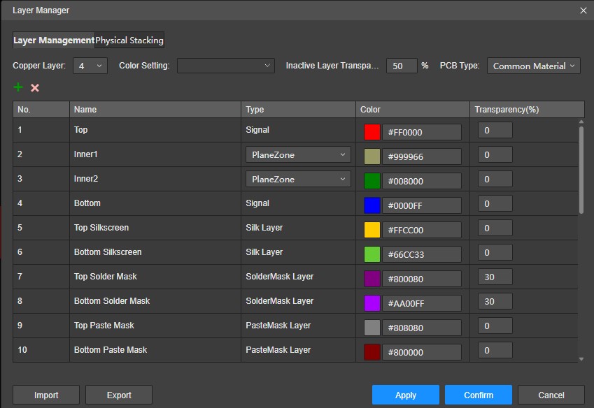
EasyEDA 中的 4-Layer PCB Stack-Up 配置。
Decoupling Capacitor Placement
Decoupling Capacitor 要发挥最佳效果,关键是缩小 Capacitor、IC Power Pin 与 Ground Plane 之间的完整 Current Loop。
Capacitance Value 很重要,但即使 Value 选择正确,如果 Placement 不佳,也可能无法有效响应快速 Transient Current。
Capacitor 应放在对应 IC Power Pin 旁边,而不是只要「位于 IC 附近」即可。
Capacitor 到 Power Pin 的 Connection 应:
- 短
- 直接
- Low Inductance
Ground Side 则应在 Capacitor Ground Pad 附近放置适当 Ground Via,让 Return Current 可以快速进入 Ground Plane,而不是经过很长的 Ground Trace。
一种常见 Layout 错误,是 Power Trace 先连接 IC,再从途中 Branch 到 Capacitor。
这种布局会让 Capacitor 位于一个 Side Branch 的末端,不利于它处理 Fast Transient Current。
更理想的方式,是让 Power Current Path 经过 Capacitor Connection 附近,再进入 IC Power Pin,从而缩短 High-Frequency Loop。
Large Bulk Capacitor 仍然非常重要,尤其是在:
- Regulator
- Connector
- Sudden Load Change Circuit
附近。
但 Bulk Capacitor 不能取代每个 IC Power Pin 附近的小型 Local Decoupling Capacitor,因为它们负责的是不同 Frequency Range 与 Current Demand。
完成 Placement 后,应检查完整 Current Loop,而不只是测量 Capacitor 到 IC 的直线距离。
Long Ground Trace、Distant Via 与 Narrow Copper Connection,即使元件在视觉上距离很近,也可能增加 Loop Inductance。
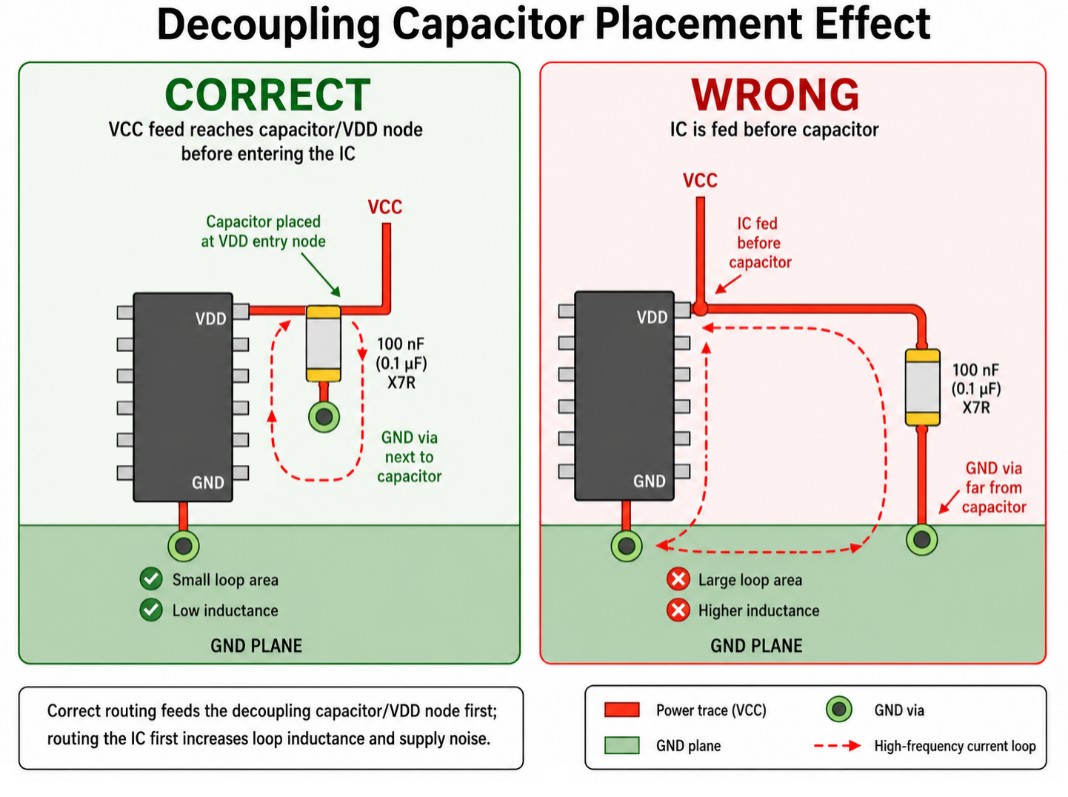
正确与错误的 Decoupling Capacitor Placement 比较。
Multi-Voltage PCB 的 Power Plane Segmentation
Multi-Voltage PCB 通常需要为不同 Power Rail 划分不同 Copper Region,例如:
- 1.2 V
- 1.8 V
- 3.3 V
- 5 V
真正困难的地方并不是「画出不同区域」,而是确保每一条 Rail 都能可靠到达其 Load,同时避免:
- Narrow Copper Neck
- Accidental Copper Island
- Critical Signal 下方出现 Reference Gap
可以先按照 Power Rail 对 Component 进行 Grouping。
这样更容易定义不同 Power Region,也可以减少不同 Board Area 之间复杂、狭窄的 Power Connection。
Regulator、Bulk Capacitor 与 High-Current Load 应尽量安排在能够形成短而清楚 Main Current Path 的位置。
重新 Pour Copper 之前,每个 Copper Region 都必须先指定正确的 Net。
之后应放大检查:
- Via
- Pad
- Mounting Hole
- Component Clearance
因为一大片 Power Region 有时实际上可能只通过一条很细的 Copper Neck 向整个区域供电。
这种 Bottleneck 可能造成:
- Voltage Drop
- Local Heating
不要让 High-Speed Signal 或 Clock Trace 跨越两个 Power Region 的 Boundary,除非 Signal 下方仍有 Continuous Ground Plane 作为 Reference。
如果 Signal 跨越的是实际 Reference Plane Split,Return Current 可能被迫绕行,导致 Noise 增加。
Release Design 前,应重新 Build 所有 Copper Area、运行 DRC,并检查最终 Gerber Output。
可以参考 JLCPCB Instructions for Ordering,确认上传最终制造文件前的相关要求。
Multi-Voltage Plane Segmentation 是很容易出现 Layout Error 的位置之一。
错误的 Boundary 或薄弱的 Copper Connection,可能直到 PCB 上电之后才被发现。
对于拥有多组 Power Rail 或 Dense Routing 的设计,可以使用 JLCPCB Layout Service,根据完成的 Schematic 协助 Placement、Routing 与 Fabrication-Aware Layout。
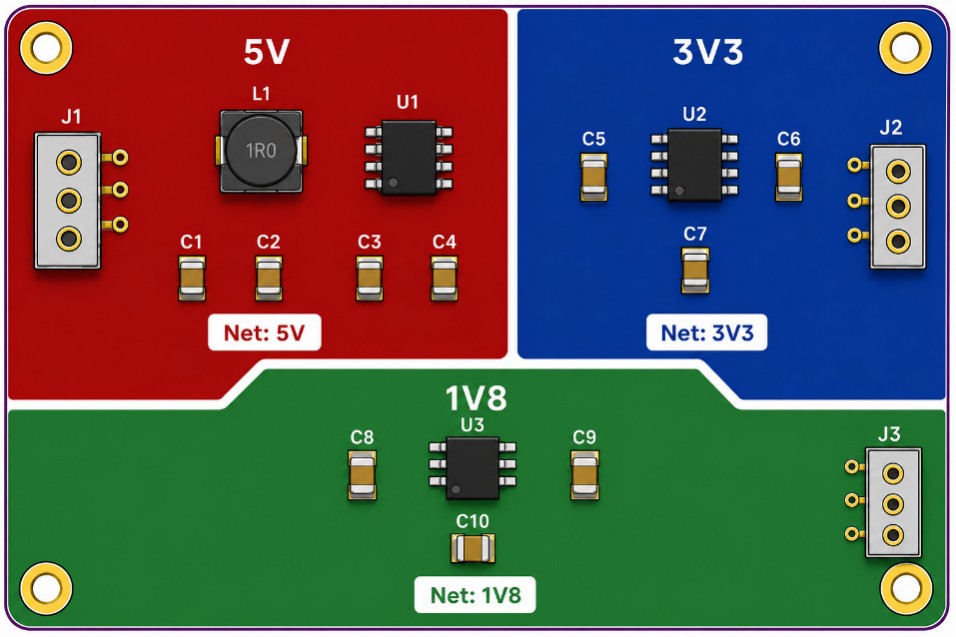
EasyEDA 中的 Multi-Voltage Power Plane Segmentation。
High-Speed 与 Mixed-Signal PCB 的 Ground Plane 设计
High-Speed 与 Mixed-Signal PCB 出现问题的常见原因,是 Layout 只按照 Circuit Type 进行区域划分,却没有考虑真正的 Current Flow。
PCB 上即使清楚标示 Analog、Digital 与 Power Section,如果不同 Return Current:
- 彼此重叠
- 穿过 Sensitive Area
仍然可能产生 Noise。
良好的 Ground Plane Design 应该从 Component Placement 开始。
将:
- Noisy Switching Circuit
- Processor
- Clock
- Communication Interface
与 Low-Level Analog Input 保持合理距离。
真正的目标并不是简单地在 PCB 上画出「Analog 区」和「Digital 区」,而是控制:
- Current 从哪里进入
- Current 从哪里返回
- 它会流经 Ground Plane 的哪些区域
Fast Digital Signal 需要 Route 在 Continuous Reference Plane 上方。
Sensitive Analog Signal 则需要避免 Switching Current 与附近较大的 Voltage Transition 干扰。
ADC、DAC 等 Mixed-Signal Component 更需要特别注意,因为 Analog Pin 与 Digital Pin 可能存在于同一个 Package 中,但对应完全不同的 Current Path。
决定 Ground Connection 时,应优先参考具体 Component Datasheet。
有些 Device 最适合使用一个 Continuous Ground Plane 并搭配良好 Placement;有些则可能明确建议 Controlled Separation 或在 Component 下方的特定位置连接。
Analog Ground vs. Digital Ground:是否需要分开?
把 Analog Ground 与 Digital Ground 分开,经常被当作固定的设计规则,但并不是所有 PCB 都适合这样做。
不合理的 Ground Split 反而可能:
- 增加 Return Path Length
- 迫使 Signal 跨越 Reference Gap
更可靠的做法通常先从 Component Placement 开始。
把 Analog Component 集中在 Analog Area,把 Digital Circuit 集中在另一个 Physical Area。
Analog Signal 尽量留在 Analog Section,Digital Signal 则留在 Digital Section。
这样可以降低 Fast Switching Current 流过 Sensitive Analog Copper 的机会。
很多 Mixed-Signal PCB 使用一个 Continuous Ground Plane,配合正确 Placement,也能得到非常好的结果。
Continuous Copper 可以让 Return Current 直接流动,避免 Ground Split 所产生的不连续区域。
关键在于不要让大量 Digital Return Current 穿过 Sensitive Analog Area。
如果 Component Manufacturer 明确要求 Ground Separation,或者 System 本身具有 Isolation Requirement,则 Split Ground 仍可能是合理选择。
这时不同 Ground Region 应在受控位置连接,同时避免 Signal 跨越 Split,除非 Return Path 也在同一位置被妥善提供。
最终决定之前,应检查:
- ADC
- DAC
- Amplifier
- Sensor
- Isolated Interface
的 Grounding Recommendation。
正确方案取决于 Device、Signal Bandwidth、Current Path 与整体 Board Architecture。
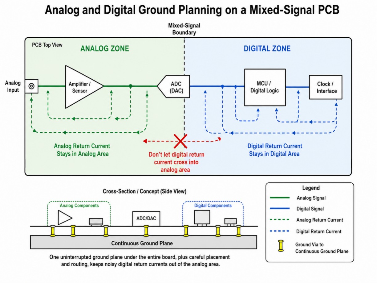
Mixed-Signal PCB 中 Analog 与 Digital Ground 的规划。
避免 Ground Loop
当 Current 存在多个回到 Source 的路径时,就可能形成 Ground Loop(接地回路)。
在单独 PCB 上,这个 Loop 可能很小。
但当 System 加入:
- Cable
- Shield
- External Power Supply
- Test Equipment
- Chassis Connection
之后,完整系统可能形成一个大得多的 Loop。
如果两个 Ground Point 的 Voltage 并不完全相同,即使只有很小的 Potential Difference,也可能驱动 Current 流过 Cable Shield 或 Signal Ground。
这些额外 Current 会在 Sensitive Measurement 中形成不需要的 Voltage,表现为:
- Hum
- Noise
- Sensor Reading 不稳定
- Communication Error
Ground Loop 经常发生在两个具有独立 Power Supply 的 Board 通过 Grounded Cable 互相连接的系统。
每块 Board 已经通过各自的 Power Supply 具有 Return Path,而 Cable 又增加了另一条 Ground Connection。
把 PCB 接到 Oscilloscope 或 Grounded Computer 时,也可能引入原本设计阶段不存在的新 Return Path。
解决方式必须从完整 System考虑,而不是只改变 PCB Ground Plane 的某一块 Copper。
需要检查所有:
- Protective Earth
- Chassis
- Cable Shield
- Power Return
- External Equipment
之间的连接。
Low-Frequency Analog System 有时可以受益于 Controlled Single-Point Connection。
High-Frequency Design 则经常需要在 Connector 附近建立短、Low-Impedance 的 Chassis Connection,而不是使用一条很长的 Wire 横跨 PCB。
Cable Shield 同样需要有意识地设计。
完全 Floating 可能降低 Shield Effectiveness,而在多个相距很远的位置直接连接,也可能形成额外 Current Loop。
正确方式取决于:
- Cable Type
- Frequency Range
- Safety Requirement
- 是否连接 Protective Earth
Release Layout 前,应把 PCB 内部与外部的完整 Return Path 都画出来检查。
很多 Ground Loop 问题实际上来自 Connector 与 Cable,而不只是 Ground Plane 本身。
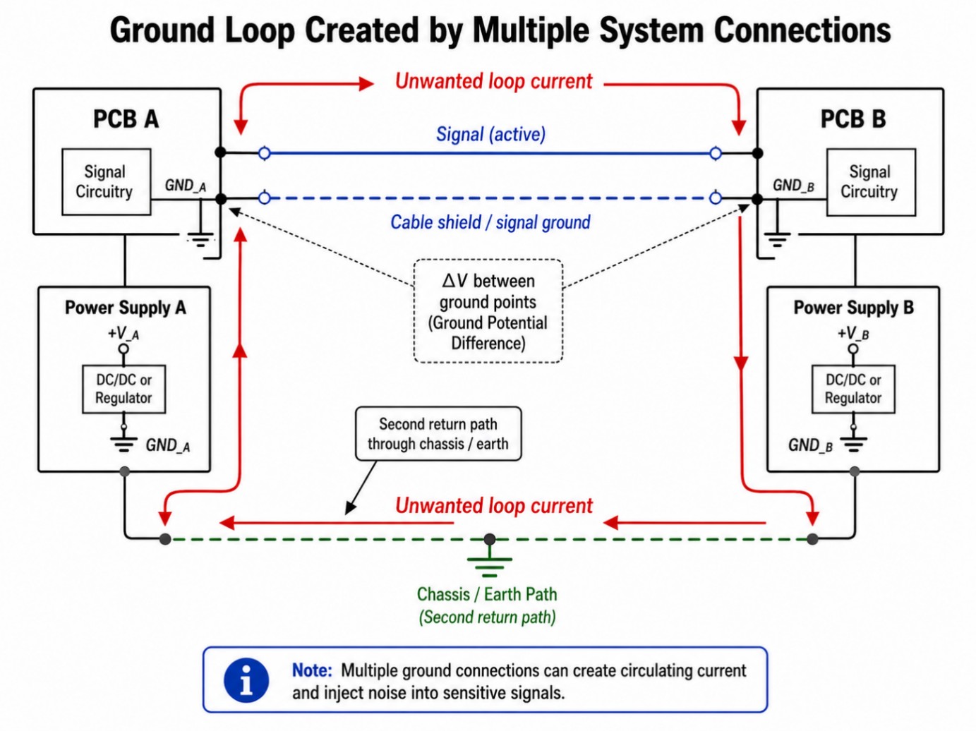
多个 System Connection 形成的 Ground Loop。
EMI Shielding 设计考量
EMI Control 首先必须从 Current Path Control 开始。
Metal Shield 或 Grounded Copper Area 可以提供帮助,但无法修复 Fast Switching Current 已经在整块 PCB 上大范围流动的 Layout。
第一优先级仍然是:
- 缩小 Noisy Current Loop
- 让每个 High-Frequency Signal 都拥有 Continuous Return Path
Shield Can 应通过周围多个短 Connection 与 Ground 连接。
一条长而窄的连接会增加 Inductance,降低 Shield 在 High Frequency 下的效果。
Shield Boundary 周围的 Ground Stitching Via 可以将 Top Copper 与 Internal Ground Plane 连接,降低 Current 从 Gap 泄漏的可能性。
Connector 同样需要特别处理。
通过 Cable 进入或离开 PCB 的 Noise,通常应在 Connector 附近尽快回到 Chassis/Ground,而不是先穿过整个 PCB。
以下元件通常也应靠近 Cable Entry Point:
- Protection Component
- Common-Mode Filter
- Shield Connection
Board-Edge Stitching Via 也可以降低 Multilayer PCB Edge 的 Radiation。
这些 Via 应将 Outer-Layer Ground Copper 与 Main Internal Ground Plane 连接。
不过 Dense Via Fence 并不能取代:
- 正确 Component Placement
- Short Switching Loop
- Continuous Reference Plane
High-Speed Area 附近也应避免留下 Isolated Copper Area。
Floating Copper Island 在 High Frequency 下可能具有不可预测的行为,并可能与附近 Trace 产生 Noise Coupling。
如果要保留额外 Copper,应有意识地将其连接至 Ground,并增加适当 Stitching Via,同时确认不会影响 Controlled-Impedance Routing。
最终 Review 时,应一起检查:
- Switching Regulator
- Clock Source
- Fast Digital Interface
- Cable Connector
- Shield Boundary
因为 EMI Problem 通常来自完整 Current Loop,而不是孤立的一条 Trace。
常见 PCB Power Plane 错误与解决方法
Power Plane 问题在 Routing 阶段不一定很明显。
Copper 可能已经连接正确 Net,Design 也可能顺利通过 DRC,但 Finished PCB 仍然出现:
- Voltage Drop
- Noise
- Local Heating
这类问题很多时候来自 Copper Geometry,而不是完全断开的 Connection。
例如:
- 某条 Narrow Copper Neck 承载整个 Circuit Block 的 Current
- Plane Boundary 正好位于 Clock Line 下方
- 多个 Via Clearance 组合成意外的 Plane Cut
这些细节在一般 Zoom Level 下很容易被忽略。
Review Power Plane 时,应把 Copper 看成Current Path,而不是单纯的 Filled Area。
从 Regulator/Connector 一路追踪每一条 Rail 到 Load,再检查其通过 Ground Plane 返回的 Return Path。
这样往往可以发现 Schematic 中完全看不到的 Weak Point。
Critical Trace 下方的 Plane Cut
Plane Cut 可能来自:
- 人为 Split
- Keep-Out Area
- Slot
- 多个 Via Clearance
如果 Fast Signal 正好从 Opening 上方经过,就可能产生严重问题。
Signal Trace 本身虽然仍然是一条直线,但 Return Current 无法继续从它正下方流过。
Return Current 必须绕过 Opening,再回到原路径。
这会增加:
- Loop Area
- Inductance
- Crosstalk
- Radiated Noise
以下 Signal 特别需要注意:
- Clock
- USB
- Differential Pair
- Memory Bus
- 其他 Fast Digital Signal
Layout Review 时,可以暂时隐藏 Signal Layer,直接观察整条 Route 下方的 Reference Plane。
不要假设 Signal Trace 看起来短,Return Path 就一定也很短。
优先解决方式,是重新 Routing,让 Signal 全程位于 Continuous Ground Reference 上方。
如果必须 Change Layer,也应维持合适的 Reference,并在 Signal Via 附近提供相应 Return Transition。
修复 Reference Path,通常比后来再增加额外 Filtering 处理衍生 Noise 更有效。
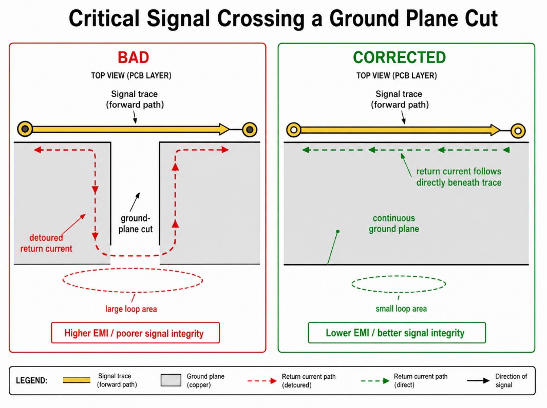
Critical Signal 跨越 Ground Plane Cut。
Texas Instruments High-Speed Interface Layout Guidelines 建议 High-Speed Signal 应位于 Solid Ground Reference 上方,而不是跨越 Plane Split 或 Void。Reference Opening 会迫使 High-Frequency Return Current 绕行,增加 Emission 并降低 Signal Integrity。
Copper Pour Coverage 不足
即使 Copper Pour 看起来覆盖了很大面积,也可能存在很弱的 Current Path。
常见情况是 Pad、Via、Mounting Hole 或 Routed Trace 周围的 Clearance,只留下很窄的 Copper Strip 连接两个大型 Copper Region。
这条 Narrow Section 可能承载整个 Circuit Block 的 Current。
随着 Current 增加,限制位置的 Resistance 会造成额外:
- Voltage Drop
- Heat
而 Plane 其他区域仍然可能保持较低温度,因此这个 Local Bottleneck 很难通过简单视觉检查发现。
尤其需要检查:
- Regulator Output
- Power Connector
- Motor Driver
- High-Current Load
- Bulk Capacitor
重新 Build Copper Pour 后,应放大这些区域,检查多个 Clearance 是否共同形成 Narrow Path 或 Isolated Copper Island。
Thermal Relief Connection 也应符合实际 Current Requirement。
Thermal Relief 可以改善 Soldering,但过窄的 Spoke 可能限制流入:
- Connector
- Power Component
- Large Pad
的 Current。
High-Current Connection 可能需要:
- 更宽的 Thermal Spoke
- Direct Copper Connection
具体方式取决于 Assembly 与 Thermal Requirement。
PCB Conductor 的 Current-Carrying Capability 不只取决于表面看到的 Width,还受到:
- Copper Thickness
- Temperature Rise
- Board Construction
- Adjacent Copper
- Operating Condition
影响。
IPC-2152 提供评估 PCB Conductor Current Capacity 与 Temperature Rise 的相关指导。
正式下单前,应直接检查 Gerber,而不是只依赖 PCB Editor。
确认每个重要 Power Region:
- 确实存在
- 连接到正确 Net
- 没有意外 Clearance
- 没有 Isolated Copper Region
同时确认 Copper Weight 与 Fabrication Option 符合 JLCPCB Ordering Requirements。
忽略 High Frequency 下的 Plane Impedance
在 Low Frequency 下,Power/Ground Plane 看起来可能只是一个简单的 Low-Resistance Conductor。
但随着 Frequency 提升,以下因素的重要性会快速增加:
- Inductance
- Capacitance
- Dielectric Spacing
- Plane Geometry
Fast Signal 不只与可见 Trace Interaction,也会受到附近 Reference Plane 影响。
即使 Trace Width 完全不变,只要 Trace 与 Plane 的距离改变,Characteristic Impedance 也会发生变化。
Plane Gap、Void 与 Layer Transition 都可能形成额外 Discontinuity。
彼此靠近的 Power 与 Ground Plane 还会形成 Distributed Capacitance。
这可以支持 Local Decoupling Network,但并不能取代 IC Power Pin 附近正确放置的 Discrete Capacitor。
Plane Capacitance 与 Discrete Capacitor 会在不同 Frequency Range 中共同工作。
Generic Impedance Equation 可以用于 Early Design,但最终 Calculation 应采用 Manufacturer 实际提供的:
- Dielectric Thickness
- Copper Thickness
- Stack-Up
可以使用 JLCPCB PCB Impedance Calculator,比较实际 Board Construction 与需要的 Trace Geometry。
Controlled-Impedance Route 应尽量保持在 Continuous Reference Plane 上方。
Signal Change Layer 时,也需要在附近提供短 Return Transition。
Route 下方任何 Plane Cut 都可能改变局部 Impedance,并增加:
- Reflection
- Timing Problem
- Radiated Noise
Circuit Board Ground Plane 常见问题
问:每一块 PCB 都需要 Ground Plane 吗?
并不是每一块简单 PCB 都必须拥有独立的 Dedicated Ground Plane Layer,但大多数 Design 都可以从大面积、连续的 Ground Copper 中受益。
当 PCB 包含 Fast Digital Signal、Switching Regulator、Communication Interface 或 Sensitive Analog Circuit 时,Solid Ground Plane 会变得更加重要。
在 2-Layer PCB 中,也可以尽可能保留其中一层作为大面积 Ground Copper,并让另一层主要负责较短的 Signal Route。
问:2-Layer PCB 可以拥有有效的 Ground Plane 吗?
可以,但需要更加谨慎地规划 Routing。
尽可能保留其中一层的大部分区域作为 Ground Copper,不要让大量 Long Trace 把它切割成许多小区域。
必要时可以使用 Ground Stitching Via 连接 Top/Bottom Ground Pour。
Routing 完成后,还要检查:
- Isolated Copper Island
- Narrow Connection
- Critical Signal 下方的 Gap
问:Analog Ground 与 Digital Ground 一定要分开吗?
不一定。
自动将 Ground Plane 分割,反而可能形成更长的 Return Path,并让 Signal 跨越 Reference Gap。
许多 Mixed-Signal PCB 使用一个 Continuous Ground Plane,并搭配谨慎的 Component Placement,反而能获得更好的结果。
Analog 与 Digital Circuit 应在 Physical Placement 上保持适当分区,避免 Digital Return Current 穿过 Sensitive Analog Area。
当 Device Manufacturer 明确建议 Controlled Split 或 Single-Point Connection 时,则应优先遵循具体 Component 的 Grounding Recommendation。
问:Ground Stitching Via 应该放多少颗?
没有一个固定数量可以适用于所有 PCB。
Stitching Via 应优先放在真正具有 Electrical Purpose 的位置,例如:
- Signal Via 附近
- Board Edge
- Connector 附近
- Shield Region
- Noisy Circuit Boundary
Via Spacing 会受到 Frequency、Board Size、Stack-Up 与 EMI Requirement 影响。
少量但位置正确的 Via,通常比大量没有明确用途的 Via 更有价值。
问:Power Plane 与 Ground Plane 可以彼此靠近吗?
可以,而且在许多 Multilayer PCB 中,这样做具有明显优势。
Power 与 Ground Plane 靠近可以降低 Power Distribution Path 的 Inductance,并在两个 Layer 之间形成一定的 Distributed Capacitance。
这可以辅助 Local Decoupling,但不能取代 IC Power Pin 附近的 Decoupling Capacitor。
实际 Dielectric Spacing 与 Layer Arrangement 必须符合 PCB Manufacturer 的 Stack-Up。
问:未使用的 Copper Area 应该连接 Ground 吗?
一般而言,Unused Copper 应有意识地连接至 Ground,或者直接移除。
Floating Copper Island 在 High Frequency 下可能与附近 Signal 产生 Coupling,并表现出不可预测的 Electrical Behavior。
如果保留 Unused Copper 并连接 Ground,应加入适当 Stitching Via,同时确认它不会:
- 形成 Narrow Clearance
- 干扰 Controlled-Impedance Trace
- 产生新的 Isolated Copper Region
Circuit Board Ground Plane 结论
可靠的 Circuit Board Ground Plane 并不只是「剩余 Copper 接到 Ground」这么简单。
它同时是 Finished PCB 的:
- Signal Path
- Power Distribution Network
- EMI Strategy
- Thermal Design
的一部分。
因此,Plane Continuity、Layer Order、Return Current Flow 与 Component Placement,都应该在 Critical Routing 开始之前就完成基本规划。
对于 High-Speed Signal,Solid Reference Plane 通常是比较安全的设计基础。
Power Region 则应检查:
- Narrow Copper Neck
- Isolated Copper Island
- Pad/Via 周围的 Weak Connection
Decoupling Capacitor 需要同时与 Power Pin 和 Ground Plane 形成短、Low-Inductance Connection。
Signal Change Layer 时,也需要为 Return Current 提供邻近且连续的 Transition Path。
正式制造之前,请:
- 重新 Build 所有 Copper Area
- 执行 DRC
- 检查 Gerber
- 确认 Stack-Up
- 确认 Copper Weight
- 比较 JLCPCB 实际 Fabrication Requirement
对于拥有多个 Power Rail、Mixed-Signal Section 或 Controlled-Impedance Routing 的复杂 PCB,也可以使用 JLCPCB Layout Service,根据完成的 Schematic 协助 Placement 与 Fabrication-Aware PCB Layout。
持續學習
電壓穩壓器 PCB:實用設計指南
重點摘要 電壓穩壓器 PCB 不只是將一種電壓轉換成另一種電壓;它還必須在處理散熱、負載變化與電路雜訊的同時,提供穩定的輸出。 佈局與穩壓器 IC 同樣重要;請將輸入與輸出電容放在引腳附近,使用短的電源連接,並確保接地回流路徑直接且具低阻抗。 線性穩壓器簡單且安靜,但會將電壓差轉化為熱量損失;當降壓幅度或負載電流較大時,開關式穩壓器是更佳選擇。 輸入與輸出電容是穩壓器系統的一部分,並非可有可無的裝飾;其容量、類型,以及在某些情況下的 ESR,都必須符合穩壓器資料表的要求。 使用 12 V 電源設計時,請在佈線前計算功率耗散,因為即使電氣上正確的電路,若穩壓器無法有效散熱,仍可能失效。 開始佈線 12 V 設計前,請使用散熱設計章節中的快速選擇表,確認你的電壓與電流組合適合線性穩壓器,還是需要散熱器或降壓轉換器。 簡介 原型在工作台上看似完美,但接上負載後可能變得不穩定;輸出可能下陷,穩壓器可能熱到無法觸摸,甚至每次馬達啟動時微控制器都會重置。在大多數情況下,真正的問題不是穩壓器本身,而是電壓穩壓器的 PCB 佈局。 良好的穩壓器設計始於正確的電路,但不止於原理圖。走線電阻、電容位置、覆銅面積、接地......
電路板接地平面與電源平面指南 2026
重點摘要 優先保持銅箔連續:完整的 PCB Ground Plane(接地平面)可以建立 Low-Impedance Return Path、降低 Noise,而且即使在 Mixed-Signal PCB 中,通常也比任意分割 Ground Plane 更安全。 從 Current Loop 思考:每一條 Signal 都需要完整的 Return Path。High-Speed Trace 不應跨越 Plane Gap、Slot 或 Cutout。 提早規劃 Stack-Up:在 Routing Critical Signal 之前先決定 Layer Arrangement,並盡量讓 Power Plane 與 Ground Plane 靠近,以降低 Power Distribution Path 的 Inductance。 Placement 比事後補 Filter 更重要:縮短 Decoupling Loop、合理配置 Stitching Via,以及妥善進行 Component Grouping,可以從 Layout 階段降低大量 EMI 與 Ground Loop 問題。 製造前再次驗證:......
LDO vs 切換式穩壓器:效率、雜訊、散熱與 PCB Layout
重點摘要 先計算 LDO 功率耗散:在比較封裝或價格之前,務必先以最大輸入電壓與最大負載計算 LDO 的功率耗散。 規格會隨工作條件改變:壓差電壓、PSRR、雜訊、紋波、效率與暫態響應都應視為與工作條件相關的參數,而不是固定不變的數值。 兩者都高度依賴 PCB 佈局:降壓轉換器的高 di/dt 輸入迴路與高 dv/dt 開關節點會產生不同的耦合機制,因此都需要仔細規劃 PCB 元件配置與走線。 輸出電容選擇:考慮容差、溫度、老化與 DC Bias 效應後,輸出電容仍必須滿足所選 LDO 對電容量與 ESR 的要求。 混合式穩壓:先使用 Buck 再串接 LDO 可以為敏感電源軌供電,但必須先確認壓差裕量、不同頻率下的抑制能力、熱耗散、啟動時序以及反向電流行為。 前言 假設需要將 12 V 輸入轉換成 3.3 V、1 A 輸出。在評估 LDO 與切換式穩壓器時,第一個真正有用的問題並不是哪一顆 IC 封裝更小,而是穩壓器必須消耗多少功率。LDO 的功率耗散約為 (12−3.3)×1=8.7 W。忽略靜態電流時,其效率約為 3.3/12=27.5%。如果降壓轉換器在此工作點假設具有 90% 效率,那麼......
LVDS PCB佈局指南:設計技巧與實作範例
重點摘要 100 Ω差分阻抗:LVDS PCB佈局從一個數值開始:100 Ω差分阻抗。走線寬度、間距與電路板厚度都會決定這個數值。 差分對同步佈線:將同一差分對的兩條走線並排佈線,並將兩者的長度差控制在5至10 mil以內。 完整接地平面:切勿讓LVDS差分對跨越接地平面的缺口,否則會中斷回流路徑並損害訊號。 至少使用4層板:具有完整接地平面的4層板足以應付大多數設計。對於尺寸較大、佈線較密集的電路板,則可使用6層板。 佈線前先驗證:開始佈線之前先檢查阻抗數值。電路板製作完成後才修正,成本會高得多。 簡介 工程師在處理器與螢幕之間接好LVDS鏈路。電路板通電後,螢幕卻閃爍或出現雜訊。 元件沒有選錯,電路圖也沒有問題,真正的問題出在銅箔走線上。這就是為什麼LVDS PCB佈局指南與電路本身同樣重要。 LVDS代表低電壓差分訊號傳輸。它使用兩條匹配的導線傳送資料,而不是使用一條訊號線及接地。這使其兼具高速與低雜訊特性。 LVDS常見於螢幕、相機及車用電子設備。如果您曾經詢問LVDS的用途,簡短答案就是:任何需要在短距離內快速傳輸資料,同時又不希望產生雜訊的地方。 LVDS本身很容易使用,但要把電路板佈......
拒絕炸板:PCB 銅厚、線寬與載流能力實務指南
一、銅厚(Copper Weight):那個被「秤重」的厚度 大家常說的 1oz、2oz 銅厚 PCB,這單位其實挺反直覺的。它不是長度單位,而是重量單位:指將一盎司(28.35克)的純銅均勻鋪在一平方英尺(約 929 平方公分)的面積上,所形成的物理厚度。 1oz = 約 35μm (1.4 mil) 2oz = 約 70μm (2.8 mil) 為什麼我們不能只靠加寬走線? 在設計馬達驅動器或高速伺服器電源時,PCB 上的空間通常被擠壓得非常厲害。如果你只有 100 mil 的寬度,卻要跑 20A 的電流,1oz 的銅基本上就是在「玩火」。這時候,把 PCB 銅厚提升到 2oz 甚至 3oz,就成了在有限空間內降低阻值、減少發熱的唯一解藥。 電阻與厚度的物理關係非常直接: 公式裡的 T(厚度)與 W(線寬)是相乘關係,銅厚翻倍,效果等同於線寬翻倍。但在 Layout 佈局上,增加厚度往往比增加線寬容易得多。 二、線寬計算機沒告訴你的「環境潛規則」 基於IPC-2221或IPC-2152標準開發的各類PCB走線寬度計算器,其計算結果均建立在理想散熱環境的假設之上。然而實際工程中,PCB多采用封閉......
走線寬度 vs 電流承載能力:電源走線的 PCB 佈局技巧
在精密的PCB 設計藝術中,電源走線是默默承載電流的無名英雄,為電路注入生命。訊號走線因阻抗匹配與雜訊控制而備受關注,電源走線則默默肩負供電重任,避免自身或所連元件燒毀。但這些走線該多寬?這正是線寬與載流能力之間的關係所在。若你認為 0.1 mm 的走線足以承受 10 A,那只不過是在設計一塊「PCB 形狀的保險絲」。想更深入了解 PCB,請參閱我們的 PCB 製造終極指南。 為何線寬在電源走線中至關重要 電源走線的核心在於高效供電,同時管理熱量、壓降與訊號完整性。線寬一旦出錯,等同於邀請熱累積、電壓跌落,甚至走線熔斷。沒錯,熔化的走線在科幻電影裡或許很酷,但在現實中只是設計災難。 IPC 已制定標準,提供測試與計算 PCB 走線溫升的方法,對應特定輸入電流。這些標準為 IPC-2221 與 IPC-2152,內含大量相關資訊。顯然,這些標準相當龐雜,多數設計師無暇逐一解析資料,只為整理出線寬對電流表。 什麼是電路板走線電阻? 自然界所有物質對電流都有一定阻力,導體與絕緣體皆會不同程度地阻礙電流。PCB 走線常以銅為導體,但銅本身成分與特性仍會產生電阻,此即 PCB 走線電阻。 電阻以歐姆為單位,......