01005 Assembly Guide: PCB Design, Stencil, Feeder Static and Reflow
18 min
- What Is an 01005 Component?
- Why 01005 Isn't Just a Smaller 0201
- PCB Design Rules That Matter at 01005
- Stencil and Solder Paste: The Short Version
- Feeder Static: Why 01005 Parts Disappear Before Placement
- Nitrogen Reflow: What It Fixes and What It Doesn't
- Inspecting 01005 Joints: SPI and AOI
- First-Pass Yield: Why 01005 Makes Rework Expensive
- 01005 vs 0201: Is the Miniaturization Worth It?
- Assembling 01005 Boards at JLCPCB
- FAQ about 01005 Assembly
Key Takeaways
01005 (imperial) parts measure 0.4 × 0.2 mm and are called 0402 in metric.
Reliable assembly rests on a flat surface finish such as ENIG, symmetrical NSMD pads, a stencil about 3 mil thick with fine paste, static control at the feeder, and 3D SPI before placement.
Because 01005 parts are slow and risky to rework, first-pass yield is the number that matters most.
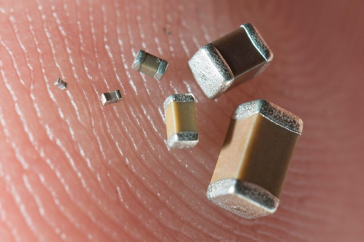
Figure: Six SMD capacitors on a fingertip, from left: 01005, 0201, 0402, 0603, 0805 and 1206. Photo: Filip Wahlberg, CC BY-SA 4.0, via Wikimedia Commons
The smallest capacitor in the photo above is an 01005: 0.4 mm long and 0.2 mm wide. Smaller sizes such as 008004 exist, but they are rare outside phone and module makers, so for most designers 01005 is the practical lower limit for passive parts. It is also the size at which several assembly rules that work at 0402 and 0201 stop working.
The reason is scaling. Shrink every dimension of an 0603 capacitor by a factor of four and you get an 01005. Its weight drops by a factor of 64. The pull of molten solder on each termination, which depends on the length of the wetted edge, drops by only about four, and static attraction, which depends on surface area, by about 16.
So relative to its own weight, an 01005 is pulled about 16 times harder by the solder, and about four times harder by static, than an 0603 is. On the line this shows up as parts that jump out of the tape, parts that stand up during reflow, and paste deposits that oxidize before they melt.
This guide skips general SMT theory and covers what changes at this size: pad design, stencil and paste, static at the feeder, nitrogen reflow, inspection, and what all of it means for first-pass yield.
What Is an 01005 Component?
01005 is an imperial size code. Read literally it suggests 0.010 × 0.005 in, but the part measures about 0.016 × 0.008 in, or 0.4 × 0.2 mm, which the metric code 0402 describes directly.
This is the most common naming trap in passive parts: 01005 imperial is 0402 metric, while 0402 imperial is 1005 metric, a part more than six times larger by area. When "0402" appears on a datasheet or BOM, check which system it refers to before ordering.
| Imperial code | Metric code | Nominal size (mm) | Relative body area |
|---|---|---|---|
| 01005 | 0402 | 0.4 × 0.2 | 1× |
| 0201 | 0603 | 0.6 × 0.3 | ~2.3× |
| 0402 | 1005 | 1.0 × 0.5 | ~6.3× |
For the full list of size codes and footprints, see our guide to SMD resistor package sizes.
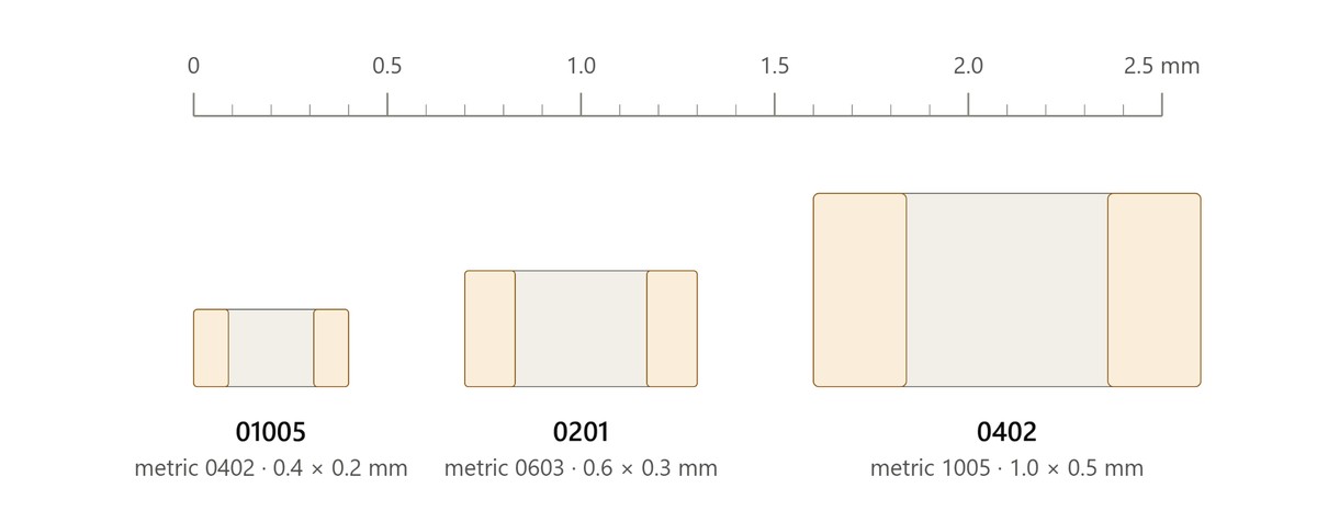
Figure: 01005, 0201 and 0402 chip outlines drawn to the same scale.
Why 01005 Isn't Just a Smaller 0201
Going from 0201 to 01005 is one step down the size chart, but it is the step where tolerances that used to sit well inside the pad start to take up a real share of it.
A typical 01005 pad is about 0.2 mm wide. Three tolerances act on it at the same time: solder mask registration on the bare board, stencil-to-board alignment at the printer, and placement accuracy at the mounter.
On a well-run line each of them is a few tens of microns. On an 0603 pad, close to a millimeter wide, a 50 µm offset is about 5% of the width and disappears into the margin.
On an 0201 pad, about 0.3 mm wide, it is already about 17%. On an 01005 pad it is a quarter of the width, and offsets from different steps can add up before any single step is out of specification.
So 01005 assembly depends less on any one special technique than on holding every step inside a tighter window at the same time.
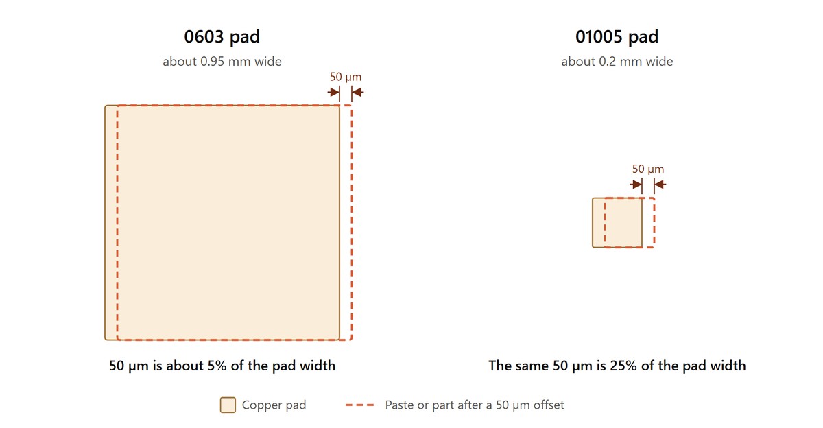
Figure: The same 50 µm offset drawn to scale on an 0603 pad and an 01005 pad.
PCB Design Rules That Matter at 01005
Surface finish
Standard HASL is a poor fit for 01005. Hot-air leveling leaves a domed, uneven solder layer, and on a 0.2 mm pad that height variation is large compared with the paste deposit printed on top of it, which is only about as thick as the stencil.
The part seats unevenly, shifts, and is more likely to tombstone. ENIG and OSP give a flat surface that suits the narrow process window. At JLCPCB, boards that carry 0201 or 01005 parts are assembled on ENIG, and the order page sets it for you. For a full comparison, see how to choose the right surface finish and HASL vs ENIG.
Pad definition
NSMD (non-solder-mask-defined) pads are the usual choice for 01005. The copper defines the solderable area and the mask opening is drawn slightly larger, so a small mask offset does not change the pad.
At this size the clearance between pad and mask opening is only a few tens of microns per side, so it is worth knowing what happens when mask and copper don't line up exactly.
While the offset is smaller than the clearance, the pad stays NSMD. Once it is larger, the mask covers the copper along one edge and that side becomes mask-defined, which changes the wetted area at that end.
JLCPCB images solder mask with LDI and supports openings down to 1:1 with the pad. Take the land pattern from the component datasheet rather than scaling down an 0201 footprint; our solder pad design guide has more background.
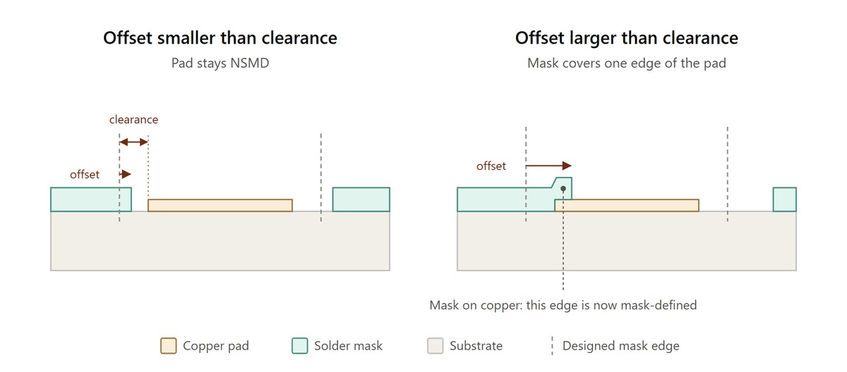
Figure: An offset smaller than the mask clearance leaves the pad NSMD (left); a larger offset puts mask on the copper and makes that edge mask-defined (right).
Thermal balance between the two pads
Uneven heating of the two pads is one of the most common causes of 01005 tombstoning. If one pad connects to a wide trace or a ground pour and the other to a thin trace, the two ends reach liquidus at different times.
The end that wets first pulls on the part, and an 01005 has almost no weight to resist it. Our guide to PCB tombstoning covers the defect in more detail.
Run the same trace width into both pads, and connect a pad to a plane through a thermal relief rather than directly. Keep vias out of the pads, with solder mask between via and pad, so that a via cannot draw solder away from one end.
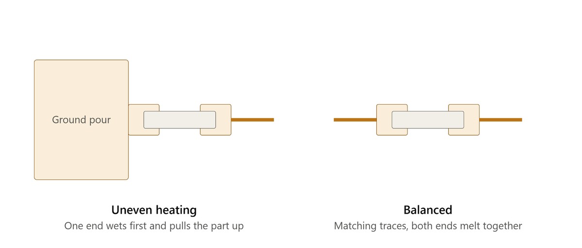
Figure: A pad tied straight into a ground pour heats more slowly, so the other end wets first and pulls the part up (left); matched traces let both ends melt together (right).
Component spacing
Tight spacing is the reason to use 01005 in the first place, but leave room for paste printing and for AOI to see every joint. A tall neighbor can block the AOI camera's angled view, and a large part right next to an 01005 can slow the heating of the nearer pad, which creates the imbalance described above.
Stencil and Solder Paste: The Short Version
Stencil design is covered in depth elsewhere, so this section deals only with what is specific to 01005.
The number that matters is the area ratio: aperture opening area divided by aperture wall area. It predicts whether paste releases onto the pad or stays in the aperture. IPC-7525 gives 0.66 as the minimum for reliable release.
Take a 0.20 × 0.20 mm aperture, typical for an 01005 pad. With a 0.10 mm (4 mil) stencil the area ratio is 0.50, well below the guideline. At 0.08 mm it rises to about 0.63, and at 3 mil (0.076 mm) it reaches about 0.66.
01005 therefore usually calls for a stencil about 3 mil thick, often nano-coated, because the coating helps paste release at low area ratios. JLCPCB offers nano-coating on every stencil type it makes; see how nano-coatings affect stencil performance.
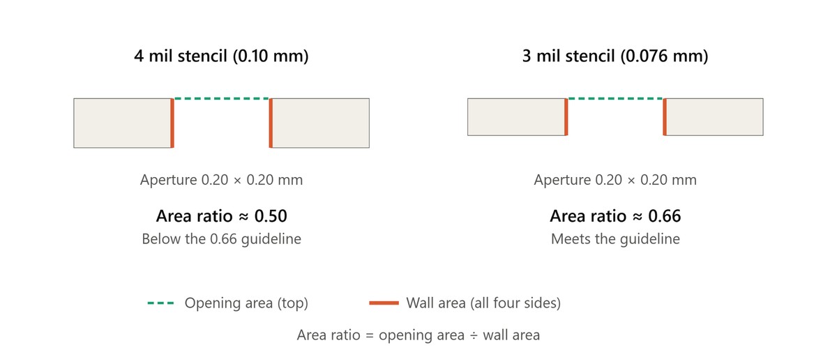
Figure: Area ratio of a 0.20 × 0.20 mm aperture: 0.50 in a 4 mil stencil, about 0.66 in a 3 mil stencil.
Paste powder size follows the same logic. A common rule of thumb is that at least five of the largest particles should fit across the narrowest aperture dimension. For a 200 µm aperture that means particles no larger than about 40 µm.
Type 4 paste (20–38 µm) sits close to that limit and can work with a well-designed aperture, but Type 5 (15–25 µm) leaves more margin, which is why it is commonly preferred for 01005. Finer powder has a cost: more particles means more surface to oxidize, which comes up again in the nitrogen section.
Mixed boards are the harder problem. 01005 passives next to a power inductor or a connector need a thin stencil, while the large parts need more paste. On many boards a single thin stencil with enlarged apertures for the large parts gives them enough.
When it doesn't, the usual answer is a step stencil, thinner around the small parts and thicker under the large ones, at extra cost and lead time. A step needs keep-out space around its edge, so plan where the 01005 parts sit relative to the large components. Our step stencil design guide covers the rules.
Feeder Static: Why 01005 Parts Disappear Before Placement
Printing and reflow get most of the attention, but 01005 parts can be lost before they reach the board at all, between the reel and the nozzle.
When the feeder peels the cover tape off the carrier tape, the separation generates triboelectric charge on the tape and in the pocket. A large part doesn't react to it. An 01005 can: the charge is enough to lift it out of the pocket, so that it sticks to the peeled cover tape, tilts onto its side, or leaves the pocket altogether.
Component makers design for this. Murata's narrow-pitch embossed tape for 01005, for example, is treated to suppress static during cover tape removal, which Murata says helps reduce pick-up errors.
On the line it shows up as pick errors, parts picked on their side, and empty positions that AOI flags after reflow. Each missing 01005 is a first-pass yield loss, and fitting a single 01005 by hand afterward is delicate work.
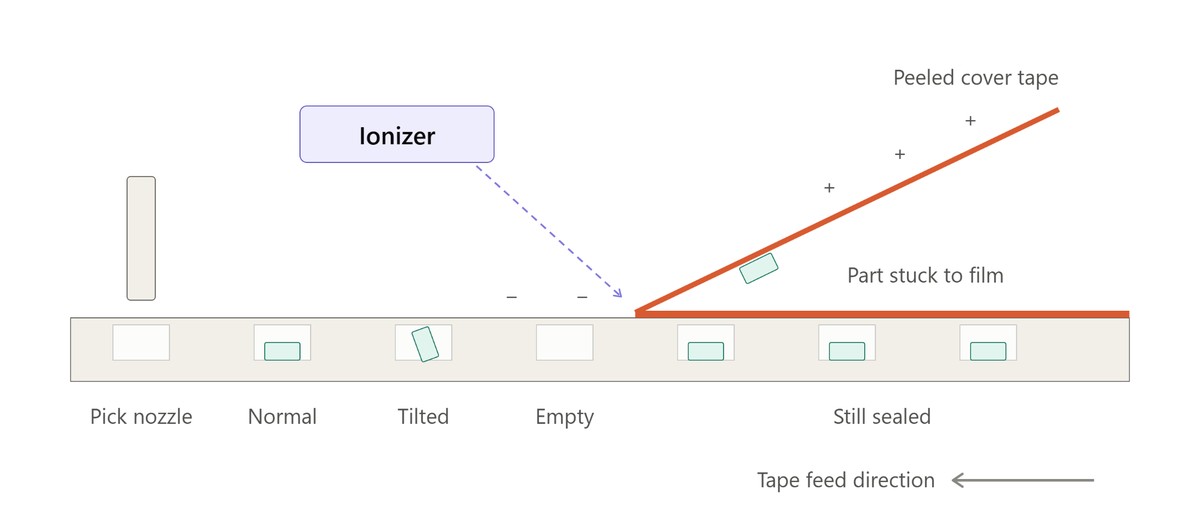
Figure: Peeling the cover tape charges the tape, so an 01005 can stick to the film, tilt in its pocket or leave it; an ionizer aimed at the peel point neutralizes the charge.
The usual countermeasure is an ionizer aimed at the feeder window, which neutralizes the charge where the tape is peeled. Peel speed and angle affect how much charge builds up, so consistent feeder setup and maintenance matter. So does humidity: very dry air lets charge accumulate more easily.
Tape type matters too. 01005 parts ship on paper carrier tape or on embossed plastic tape like Murata's, and the two behave differently at the feeder. When one reel gives trouble and another doesn't, check the tape first.
A mounter's placement accuracy cannot help if the part is already tilted in its pocket when the nozzle arrives, which is why static control matters as much as the mounter at this size.
Nitrogen Reflow: What It Fixes and What It Doesn't
Every joint sees some oxidation during reflow, but 01005 deposits are more exposed for two reasons. A small deposit has more surface for its volume, so its flux dries out and is used up sooner during preheat.
And the fine powder it is printed with contains more particles, each with its own oxide layer for the flux to remove. When oxidation outruns the remaining flux, the particles don't fully coalesce, and the result is graping: a joint that looks like a cluster of partly fused spheres instead of a smooth fillet.
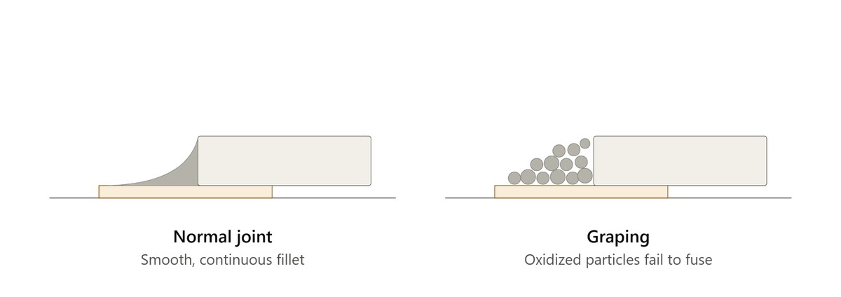
Figure: A normal joint with a continuous fillet (left) and graping, where oxidized particles fail to fuse (right).
Reflowing in nitrogen leaves less oxygen to react with the solder, which reduces oxidation and improves wetting. For deposits this small it widens the process window. JLCPCB lists nitrogen reflow among its assembly processes. For the basics of the process, see our reflow soldering guide.
Nitrogen does not fix tombstoning, and it can make it worse. With less oxidation the solder wets faster, so surface tension starts pulling on the part sooner; Indium Corporation makes this point in its note on minimizing tombstoning.
If one pad reaches liquidus before the other, that faster pull is more likely to stand the part up. A two-phase design-of-experiments study of 0201 tombstoning by Neathway et al., run in the late 2000s mostly with Type 3 paste and 100 ppm nitrogen, found the same trade-off: reflow in air produced fewer tombstones than nitrogen but more defects overall, including skewed parts and non-wets.
The reflow profile is a trade-off as well. A soak brings small and large parts closer to the same temperature before the solder melts, which is the textbook fix for tombstoning on mixed boards, and the 0201 study above treated the straight ramp as the worse of its two profiles.
It also gives the flux in each 01005 deposit longer to dry out, which pushes toward graping. Indium Corporation calls a straight ramp to peak the favorite profile today and adds a soak only when the board can't be heated evenly without one, which is the usual case on boards with large differences in thermal mass.
Either way the profile is set per board, from thermocouple data and the paste datasheet. Our reflow soldering profile article walks through each stage.
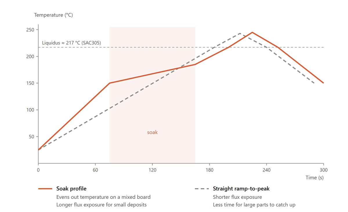
Figure: Soak versus straight ramp-to-peak: the soak evens out board temperature, the straight ramp keeps flux exposure short.
Inspecting 01005 Joints: SPI and AOI
Many 01005 defects start at the printer, so solder paste inspection (SPI) is the most useful inspection step here. A 3D SPI system measures the height and volume of every deposit and catches insufficient paste, bridging and offset before a part is placed, while the fix is still a board clean and a reprint. JLCPCB's Standard PCBA includes 3D SPI; our solder paste inspection guide explains how it works.
After reflow, automated optical inspection (AOI) checks for missing parts, tombstones, shifts and bridges. 2D AOI works from images, and on a joint this small a partly lifted termination can look much like a good one from directly above.
3D AOI adds height measurement, which makes lifted ends and partial tombstones much easier to catch. Both JLCPCB PCBA services include AOI.
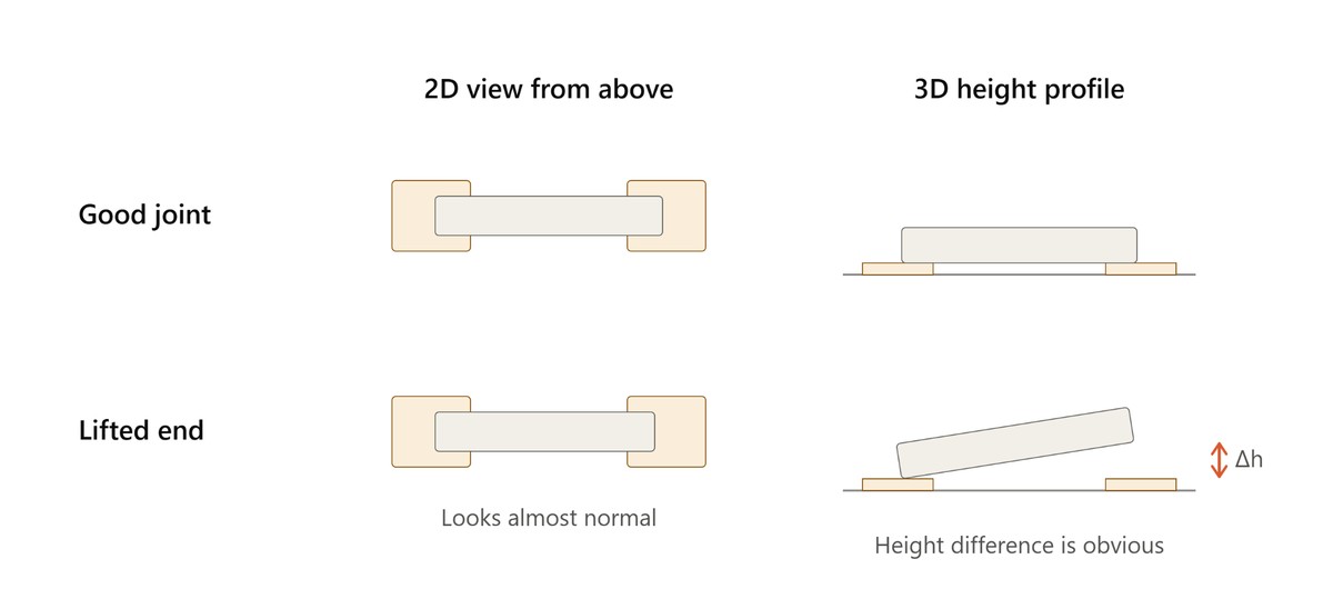
Figure: A lifted 01005 end looks almost normal in a 2D top view but shows a clear height difference in a 3D profile.
Because 01005 terminations are visible from above, optical inspection is the primary method. X-ray is for joints hidden under BGA, QFN and LGA packages, as described in our PCB X-ray inspection guide.
First-Pass Yield: Why 01005 Makes Rework Expensive
Here, first-pass yield (FPY) means the share of boards that pass the defined production and inspection steps without rework. It matters more for 01005 than for most sizes because rework is slow and risky: hot air strong enough to reflow one part easily disturbs its neighbors, so a defect that is a quick touch-up at 0603 becomes a careful repair at 01005.
FPY is a board-level figure: one bad part fails the whole board. Part-level quality is usually given in DPPM (defective parts per million), and the two are linked more closely than they first appear.
Take a board carrying 500 parts, all 01005, and assume defects are independent. At 100 DPPM the chance that a board has no defective 01005 is (1 − 0.0001)500, about 95%. At 20 DPPM it is about 99%. On dense boards, small gains in part-level quality show up directly in FPY.
When yield is lost, it usually falls into one of four groups.
| Defect | Usual causes | Main controls |
|---|---|---|
| Tombstoning | Uneven pad heating, placement offset, unequal paste volume | Symmetric pads and traces, reflow profile |
| Bridging | Excess paste, print offset, tight spacing | Aperture design, 3D SPI |
| Insufficient solder or poor wetting | Poor paste release, oxidation | Area ratio, finer paste, nitrogen reflow |
| Missing or side-placed parts | Static at the feeder, tape type | Ionizers, humidity control, tape choice |
Our guide to solder bridging covers the second group in more depth.
01005 vs 0201: Is the Miniaturization Worth It?
| Typical process considerations | 01005 | 0201 |
|---|---|---|
| Nominal size | 0.4 × 0.2 mm | 0.6 × 0.3 mm |
| Typical stencil thickness | About 3 mil (0.076–0.08 mm); step stencil on mixed boards if needed | 3–4 mil (0.076–0.10 mm) |
| Typical paste | Type 5 (Type 4 possible) | Type 4 (Type 3 possible) |
| Feeder static sensitivity | High | Moderate |
| Nitrogen reflow | Often beneficial | Can be beneficial |
| Rework | Very difficult | Difficult |
| Main benefit | Maximum density | Density with a wider process window and easier handling |
The board area saved by moving from 0201 to 01005 is usually smaller than the body sizes suggest, because spacing rules, routing and via placement become the limit first.
01005 earns its place where every square millimeter counts: hearing aids, earbuds, smartwatches, camera modules, compact wireless modules and RF matching networks. Our guide to wearable PCB assembly covers more of these designs.
If 0201 fits the layout, it gives a wider process window and easier rework. When 01005 is on the table mainly because it is the smallest size available, lay the board out in 0201 first and see how much space 01005 would save.
Assembling 01005 Boards at JLCPCB
At the time of writing, JLCPCB assembles 01005 parts under Standard PCBA, and Economic PCBA goes down to 0402; both limits are listed on the PCB assembly capabilities page.
01005 resistors, capacitors and inductors are stocked in the JLCPCB parts library, where they are marked Standard Only. For boards that mix 01005 with much larger parts, JLCPCB recommends evaluating a step stencil so that each part gets the paste volume it needs.
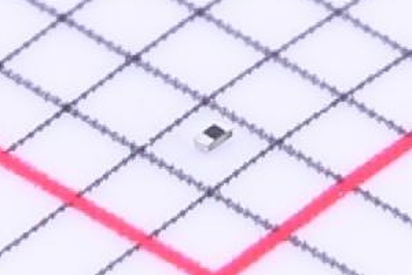
Figure: An 01005 resistor (C270305) in its JLCPCB parts library photo; one grid square is 1 mm.
Before ordering, run your files through JLCDFM, our free DFM check, then check two things by eye: that both pads of every 01005 connect symmetrically, and that the footprints come from the component datasheets rather than a scaled-down 0201.
When the design is ready, upload the Gerber, BOM and CPL files to get an instant PCB assembly quote.
FAQ about 01005 Assembly
Q: How big is an 01005 component?
An 01005 part measures 0.4 × 0.2 mm, or about 0.016 × 0.008 in. In metric naming it is 0402, which is easy to confuse with imperial 0402, a 1.0 × 0.5 mm part more than six times larger by area.
Q: Why do 01005 components tombstone?
Tombstoning happens when the two terminations wet at different times or with different force, pulling one end of the part upright. An 01005 is so light that a small imbalance will do it: unequal pad connections, a placement offset or uneven paste volume. Nitrogen reflow can make it worse, because it speeds up wetting.
Q: What solder paste is used for 01005?
Type 5 (15–25 µm) is commonly preferred, because its finer powder prints more reliably through the small apertures 01005 needs. Type 4 (20–38 µm) can work with a well-designed aperture but leaves less margin.
Q: What stencil thickness is used for 01005?
Usually about 3 mil (0.076–0.08 mm), which keeps the area ratio of a 0.2 mm aperture close to the 0.66 guideline. Nano-coated stencils release paste better at low area ratios. Boards that mix 01005 with large parts may use enlarged apertures for the large parts or a step stencil.
Q: Can 01005 components be hand soldered?
It can be done under a microscope with very fine tools, but the results are hard to repeat. Beyond one-off prototype repairs, machine assembly is the realistic option.
Q: Does JLCPCB support 01005 assembly?
Yes. 01005 is supported under Standard PCBA. Economic PCBA supports packages down to 0402.

Upload your Gerber, BOM and CPL files on the quote page; 01005 parts are assembled under Standard PCBA.
Run your files through JLCDFM, our free DFM check, before you order.
Popular Articles
• SMT Assembly Process Explained and Equipment Used: A Step-by-Step Guide to PCBA Manufacturing
• Common PCB Assembly Methods and Soldering Techniques Explained
• SMD Soldering Tools You Need: Complete Guide from Beginner to Pro
• What Is BGA Void? Causes, IPC Limits, and Solutions
• Reflow Soldering: Everything You Need to Know
Keep Learning
01005 Assembly Guide: PCB Design, Stencil, Feeder Static and Reflow
Key Takeaways 01005 (imperial) parts measure 0.4 × 0.2 mm and are called 0402 in metric. Reliable assembly rests on a flat surface finish such as ENIG, symmetrical NSMD pads, a stencil about 3 mil thick with fine paste, static control at the feeder, and 3D SPI before placement. Because 01005 parts are slow and risky to rework, first-pass yield is the number that matters most. Figure: Six SMD capacitors on a fingertip, from left: 01005, 0201, 0402, 0603, 0805 and 1206. Photo: Filip Wahlberg, CC BY-SA 4......
How to Repair a PCB: Traces, Pads, Solder Joints and Corrosion
figure: reworking an SMD joint with a soldering iron and tweezers A cut trace, a lifted pad or a joint that cracked after two years of thermal cycling doesn't mean the board is scrap. Most surface-level circuit board damage can be fixed with an iron, a multimeter and an hour at the bench. This guide covers finding the fault, the five most common repairs, and testing the board before it goes back into service. Each repair is broken into the steps you perform, in order, with the mistakes that most often......
How to Solder Wires to a Circuit Board Properly: Step-by-Step Guide
Learning how to solder wires to a circuit board is a fundamental skill for electronics repair, prototyping, and PCB assembly. Whether you are attaching power leads, signal wires, or test connections, a weak solder joint can cause intermittent failures, lifted pads, or long-term reliability issues. In this step-by-step guide, you'll learn the correct tools, preparation methods, and soldering techniques needed to create strong, clean, and reliable wire-to-PCB connections. From preparing the wire and PCB......
PCB Soldering Basic Techniques and Overview
Soldering means joining metal components with a melted metal called solder, which has a low melting point compared to other metals. Soldering is crucial in the electronics industry and is the primary method of joining electrical components. There are different types of soldering materials based on quality and their melting points. The most common combination is a tin or lead metal alloy mixed with silver or brass. The soldering iron melts the metal so it can be used like glue to connect two pieces. On......
SMT Assembly Process Explained and Equipment Used: A Step-by-Step Guide to PCBA Manufacturing
Today's high-performance electronics, from pocket-sized smartphones and IoT sensors to sophisticated industrial control systems, are made possible by a manufacturing miracle: Surface Mount Technology (SMT). SMT is the backbone of electronics manufacturing, allowing us to have the incredible component density and miniaturization. A bare circuit board is simply a substrate. The process of transforming it into a functional electronic circuit is known as Printed Circuit Board Assembly. This article outlin......
Common PCB Assembly Methods and Soldering Techniques Explained
Whether you're designing your first prototype or scaling up to production, understanding PCB assembly methods and soldering techniques is crucial to achieving reliable, high-performance circuit boards. Modern PCBA primarily relies on Surface Mount Technology (SMT) and Through-Hole Technology (THT)—each offering unique advantages for component density, durability, and manufacturability. In this guide, we'll break down the major PCB assembly methods, key soldering techniques such as reflow and wave sold......