
Solder Paste Inspection (SPI): A Complete Guide to Process Control in SMT Assembly
16 min
- What is Solder Paste Inspection (SPI)?
- Why Solder Paste Inspection (SPI) is Critical in the SMT Assembly Process
- How Solder Paste Inspection Works?
- Solder Paste Inspection (SPI) Data Parameters
- 2D vs 3D SPI (Solder Paste Inspection)
- Core Elements of Solder Paste Inspection (SPI) Machines
- Typical Defects Identified by Solder Paste Inspection (SPI)
- Factors Affecting SPI Accuracy & Solder Paste Printing Quality
- Integration of Solder Paste Inspection (SPI) in SMT Lines
- Data and Statistical Process Control (SPC) in Solder Paste Inspection (SPI)
- Best Practices to Improve Solder Paste Inspection (SPI) Accuracy
- Comparison: SPI vs AOI (Automated Optical Inspection)
- Partner with JLCPCB for Consistent, High-Quality SMT Assembly
- Future Trends in Solder Paste Inspection (SPI)
- FAQ about Solder Paste Inspection (SPI)
- Conclusion: Solder Paste Inspection (SPI)
In today's Surface Mount Technology (SMT) manufacturing world, the consistency of the solder paste deposit is the element that drives electrical performance, mechanical shear strength, and long-term reliability of assembled Printed Circuit Boards.
The solder paste is the medium that bonds the component terminations to the copper pads on the PCB. Therefore, any variations in the solder paste deposit in terms of volume, thickness, or placement will drastically impact the quality of the solder joints in the end product.
What is Solder Paste Inspection (SPI)?
Solder Paste Inspection (SPI) is an advanced quality control process that occurs right after the stencil printing process but before the placement process begins. The inspection includes verification of crucial solder paste characteristics, such as height, area, volume, and placement accuracy of all solder pads on the PCB. SPI maintains each deposit to within the acceptable tolerance levels and helps highlight process errors before defects begin to manifest—long before they become expensive.
A good solder joint starts with the right print of solder paste. It only takes a small misprint, such as a slight misalignment or low volume of paste, to create defects like tombstoning, bridging, poor solder wetting, or open circuits after reflow. Active misprints not only lower the yield of the product but also create the potential for field failures and warranty costs if they are not resolved.
State-of-the-art SPI machines currently feature 3D optical scanning capabilities that measure each solder deposit with sub-micrometer accuracy, while providing real-time feedback and data to engineer continuous improvement in the process. Engineers can adjust in near real-time, and without great effort, multiple stencil printer parameters such as squeegee pressure, speed, and squeegee alignment to achieve accelerated stabilization and adaptation during the production process.
Why Solder Paste Inspection (SPI) is Critical in the SMT Assembly Process
In SMT assembly, solder paste printing is one of the most critical steps affecting the reliability of the final PCB. Research indicates that over 60% of defects in SMT assembly originate from solder paste printing, including insufficient solder volume, bridging, or misaligned deposits, all of which can cause open circuits or shorts after reflow.
Solder Paste Inspection (SPI) serves as the first line of defense, immediately verifying each solder deposit for height, volume, area, and placement accuracy. By detecting deviations early, SPI prevents defective boards from progressing to component placement and reflow, allowing engineers to implement corrective actions before assembly continues. This early intervention reduces process variation, minimizes rework, and ensures higher product reliability.
Key Benefits of Implementing SPI on SMT Lines
- Early Defect Detection – Identifies printing errors immediately after stencil printing, ensuring only boards with accurate solder deposits proceed to placement and reflow.
- Yield and Reliability Improvement – Correcting defects at the source reduces scrap, rework, and potential field failures, directly enhancing production yield.
- Process Control and Optimization – SPI systems provide SPC data, enabling engineers to monitor trends and continuously adjust printing parameters for optimal process performance.
- Improved Traceability – Each inspection generates an electronic record, supporting quality audits, defect investigations, and customer reporting.
- Cost and Time Savings – Early detection of printing issues reduces wasted materials, prevents downtime, and improves overall production efficiency.
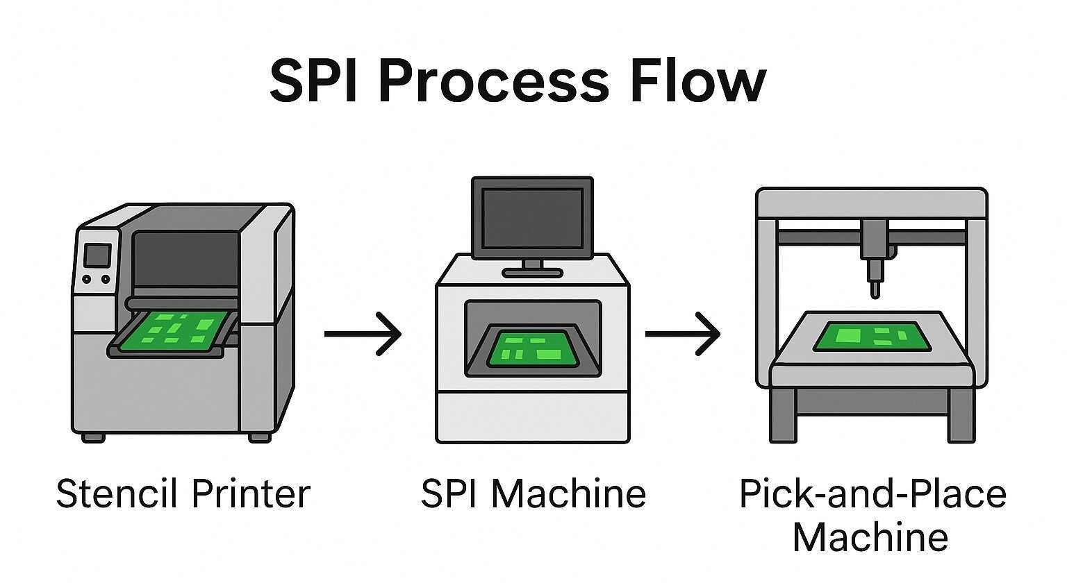
How Solder Paste Inspection Works?
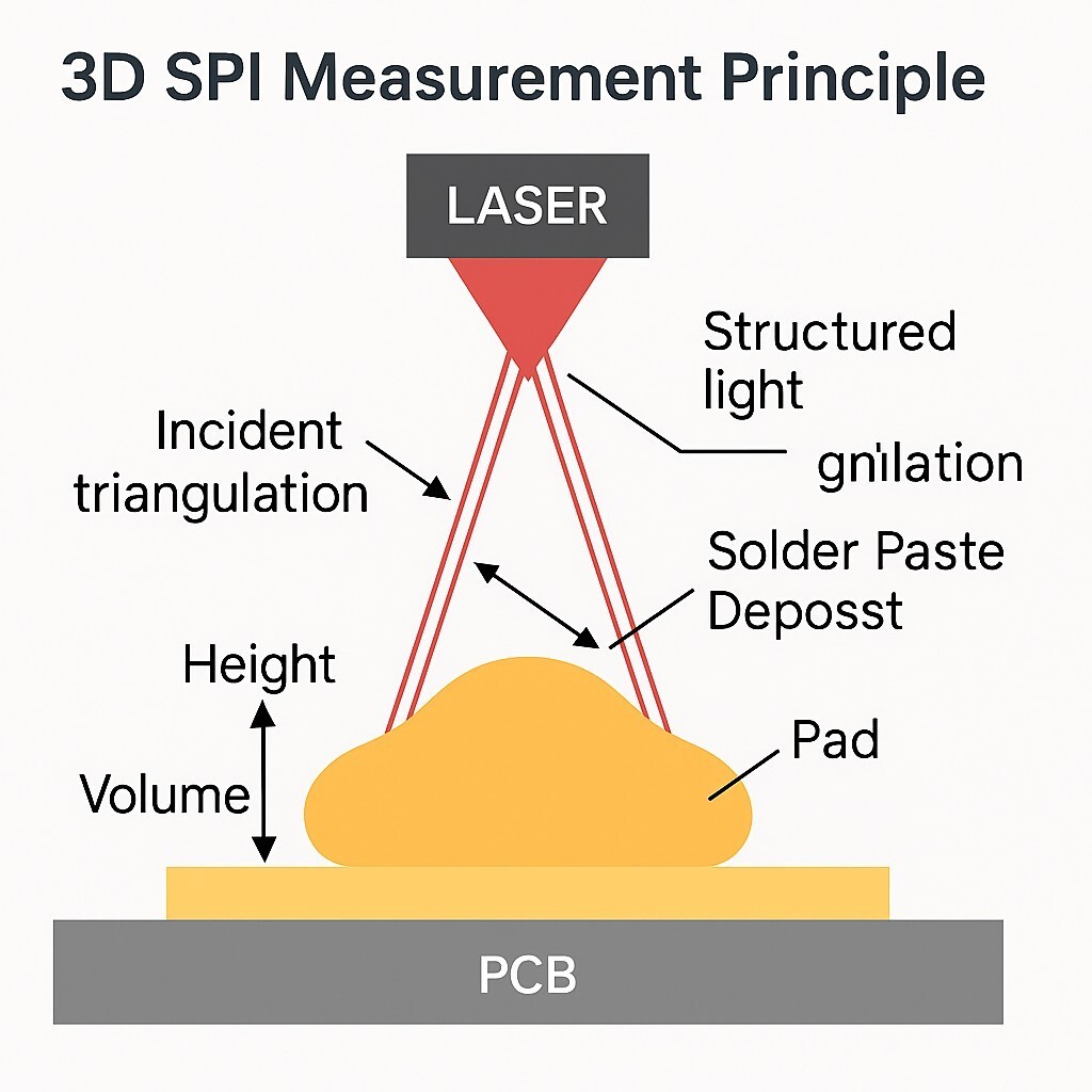
A Solder Paste Inspection (SPI) system functions as an automated 3D measurement and analysis tool to verify the accuracy of solder paste deposition in the Surface Mount Technology (SMT) process. The operation takes place through the use of structured-light projection or laser-based scanning to measure the shape of each solder paste deposit and compare it to the target design data.
The SPI system will provide assurances that every pad has received the correct paste volume, that paste deposits are correctly aligned, and that the height of the paste deposits is acceptable before components are placed.
Next is a description of how SPI systems operate in a modern SMT production line as a step-by-step activity:
-
Stencil Printing
The process begins when solder paste is printed onto the PCB through stainless steel stencil apertures with the aid of a squeegee blade. The printed paste volume is a function of the aperture size, stencil thickness, printing speed, and viscosity of the paste. Any of those factors being inconsistent can cause defects in bridging or insufficient solder.
-
Transport to SPI
After the stencil printing, the PCB will automatically transfer from the stencil printer to the SPI machine. This helps avoid handling errors and allows evaluation of the PCB before the solder paste dries and/or deforms.
-
3D Imaging and Measurement
SPI projects defined light patterns or laser stripes onto the printed solder paste, and triangulation principles that evaluate the displacement of the reflection from the lights. This creates a very precise 3D height map of each solder deposit and captures millions of data points per second.
-
Data Analysis and Comparison with the CAD or Gerber Data
SPI measures paste height, area, volume, and positional accuracy, and compares the data with relevant CAD or Gerber data to evaluate if each pad is within the acceptability tolerances.
-
Results Classification and Feedback
SPI classifies defect types such as an insufficient paste volume, excessive paste, offset prints, bridging, or shape deformation, and offers some visual analysis feedback to operators to assist in evaluating specific pads/areas.
Solder Paste Inspection (SPI) Data Parameters
| Parameter | Description | Tolerance |
|---|---|---|
| Paste Height | Vertical thickness of solder paste | ±20 % of target |
| Paste Area | 2D footprint area on pad | ±25 % |
| Paste Volume | Calculated = Height x Area | ±15 % |
| Position Offset | X/Y misalignment between the paste deposit and the center of the pad | ≤ 50 µm |
| Shape / Area Ratio | Deviation from expected geometry | < 10 % |
Note
By monitoring these measurements, you can achieve repeatable solder joints after reflow.
2D vs 3D SPI (Solder Paste Inspection)
| Feature | 2D SPI | 3D SPI |
|---|---|---|
| Measurement Type | Optical grayscale | Laser/structured-light depth measurement |
| Output Data | Area, offset | Height, area, volume |
| Accuracy | Moderate | High (±1 µm) |
| Cost | Lower | Higher |
| Best use | Prototype Continuous line | Automated mass production |
3D SPI is used in nearly all modern SMT lines due to its volumetric measures, along with closed-loop control between the printer and inspection system.
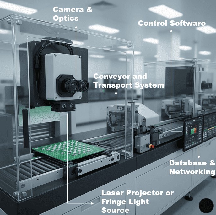
Core Elements of Solder Paste Inspection (SPI) Machines
A Solder Paste Inspection (SPI) system integrates optical, mechanical, and computational components to ensure precise solder paste deposition during Surface Mount Technology (SMT) assembly.
Each element collects, analyzes, and processes data to guarantee consistent and repeatable solder printing quality. The main components of an SPI system include:
1Camera & Optics
The camera module is the core of the SPI system, typically featuring high-resolution 2D and 3D cameras. These cameras capture solder paste images from multiple angles. 3D SPI systems use optical triangulation or fringe projection to reconstruct the height and volume of solder deposits with micrometer-level precision. The optical system must maintain focus and proper lighting across varying PCB surfaces to ensure accurate measurements.
2Laser Projector or Fringe Light Source
Structured light is typically projected, in modern SPI systems, either as a laser stripe or as a digital fringe pattern to collect depth information. When projected onto the solder paste surface, the light pattern is deformed based on the height of the paste. The camera analyzes this deformation to provide a 3D height map of the paste. The performance of this subsystem is a direct influence on measurement accuracy and repeatability.
3Conveyor and Transport System
A motorized conveyor system integrates the SPI machine into the SMT line, moving PCBs automatically from the stencil printer to the pick-and-place machine. Proper alignment ensures minimal handling and maintains board integrity throughout the production flow.
4Control Software
The SPI software functions as the system's brain, handling image processing, defect detection, and statistical process control (SPC). Advanced systems offer real-time defect visualization and can automatically adjust printing parameters, such as stencil cleaning intervals and print pressure, to optimize the process.
5Database & Networking
All inspection results are preserved in a central database for establishing traceability and optimizing the overall process. Networking capabilities enable engineers to observe several systems simultaneously (multiple SPI systems), observe long-term trends, and transfer data to manufacturing Execution Systems (MES) for full transparency on production.
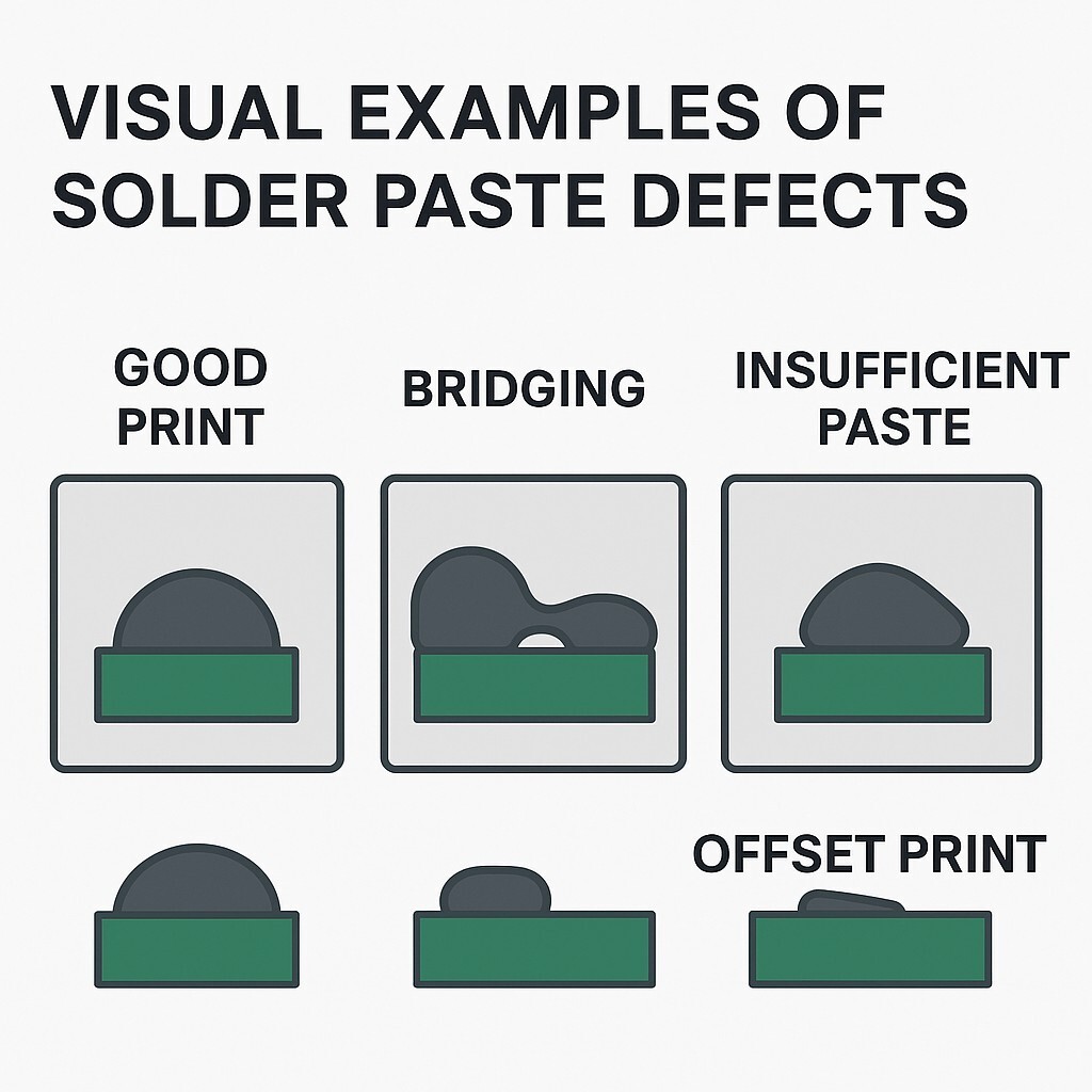
Typical Defects Identified by Solder Paste Inspection (SPI)
Early detection of these defects through SPI minimizes downstream rework and improves overall assembly yield.
| Defect Type | Definition | Process Source |
|---|---|---|
| Not Enough Paste | Insufficient amount of solder | Clogged stencil aperture |
| Too Much Paste | Depositing too much solder | Damaged stencil apertures or excessive squeegee pressure leading to over-deposit. |
| Bridging | Paste connecting adjacent pads | Incorrect paste volume or stencil issue |
| Offset Print | The deposits misaligned | Board-to-stencil misalignment / registration error. |
| Shape Deformation | Paste deposit geometry deviates from the expected profile | Uneven squeegee pressure, stencil wear, or improper release. |
Factors Affecting SPI Accuracy & Solder Paste Printing Quality
Solder Paste Printing Quality Factors
- Thickness of Stencil & Design of Aperture: This influences the amount of solder and is determined by the component pitch.
- Viscosity of Solder Paste & Storage: The rheology (viscosity and thixotropy) of the paste is critical. Improper rehydration, mixing, or storage can lead to slumping, poor definition, or clogging.
- Pressure & Speed of Squeegee: Excessive pressure can cause incomplete paste release (leading to insufficient solder) and accelerate stencil wear. Too little squeegee pressure may yield a print that doesn't fill the stencil.
- Flatness & Support of PCB: Warpage will disallow the PCB from lining up or missing the deposit of paste altogether.
- Environmental Conditions: Temperature shall be controlled between 25±3°C, and humidity between 45-75% RH.
Environmental Factors & Maintenance
To facilitate consistent SPI measurement outcomes, it is necessary to ensure that:
- Optics are kept clean and free of dust.
- Z-axis height sensors should be calibrated weekly.
- Room temperature and humidity are stable;
- Software is maintained and up to date for algorithm precision.
Scheduled maintenance minimizes false defects and extends the overall life of the equipment.
Human Factors and Operator Training
Although SPI has significant automation capabilities, human factors remain extremely valuable. Operators must be able to interpret 3D data, determine root causes of defects, and provide recommendations for adjustments to the printing parameters.
Ongoing training and certification programs provide the ability to keep the automation in place while at the same time minimizing human factors.
Integration of Solder Paste Inspection (SPI) in SMT Lines
Maintaining consistent solder paste quality in a modern surface mount technology (SMT) production line is essential in achieving high assembly yields. The general SMT process involves six steps:
- Solder Paste Printer
- Solder Paste Inspection (SPI)
- Pick-and-Place Machine
- Reflow Oven
- Automated Optical Inspection (AOI)
- In-Circuit Testing (ICT)
Solder Paste Inspection (SPI) is in sequence after the stencil printing process and before any component placement. This enables manufacturers to verify that solder paste quality meets the stated requirements while there is still sufficient time to make corrections, ensuring that no defective boards proceed to the next phase.
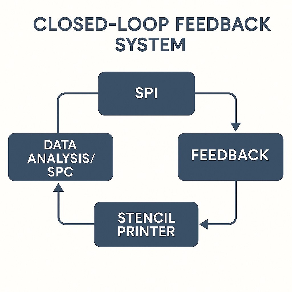
Modern SPI systems are integrated into the production control of the SMT line. If a defect is found, such as insufficient solder volume, offset printing, or bridging, the SPI system communicates directly with the solder paste printer and may automatically adjust the squeegee pressure or speed, and/or initiate a stencil cleaning process to eliminate the defect.
This is a closed-loop feedback system, which continuously monitors the solder printing process to stabilize it as well. As a result, SPI not only prevents defective assemblies but also increases process repeatability, line efficiency, and long-term yield performance.
Data and Statistical Process Control (SPC) in Solder Paste Inspection (SPI)
Modern 3D Solder Paste Inspection (SPI) systems do far more than detect defects—they function as high-resolution data acquisition platforms. Every PCB scanned generates detailed measurement data for each pad, including solder paste height, area, volume, and positional offset.
This real-time dataset forms the foundation of Statistical Process Control (SPC), which monitors process stability, reveals long-term trends, and helps engineers correct printing deviations before defects occur. With SPC, manufacturers can verify print consistency, evaluate equipment performance over time, and maintain tight control limits required for advanced SMT production.
Common SPC Metrics within SPI Systems
- Cp/Cpk (Process Capability/Performance Indices): These indices measure the ability of the solder paste printing process to output within the specification limits (tolerances). A high Cp indicates low process variation relative to the wide specification. Cpk is a more critical metric as it also accounts for how centered the process is within the specifications. High Cpk values are required for robust, high-yield production.
- Average Volume Trend: Gradual declines in paste volume, which may be caused by either stencil wear, drying of the paste, or incorrect squeegee pressure, can be tracked.
- False Reject Rate (FRR): This trending metric provides valuable information about the reliability and accuracy of the algorithms used by SPI inspection processes.
- Defect Distribution Analysis: Helpful for engineers to visualize a defect and its frequency/location while also highlighting areas that are consistently defect-prone to a specific zone on a particular PCB.
Best Practices to Improve Solder Paste Inspection (SPI) Accuracy
For results to be repeatable and dependable, solder paste inspection (SPI) must take place in standardized conditions with controlled processes. Best practices enable manufacturers to maintain uniform solder quality while preventing process drift in high-volume surface mount technology (SMT) lines.
- Establish Standard Acceptance Criteria: Define measurement limits for solder paste height, area, and volume based on component type. To ensure a uniform evaluation of solder paste inspection results according to standard evaluation criteria, the subjective nature of the evaluations is decreased.
- Regular Calibration of SPI Systems: Regularly calibrating your SPI systems ensures accurate 3D measurements and eliminates long-term system drift for precision.
- Use Statistical Process Control: Utilize real-time statistical process control (SPC) to identify variation in your process, observe process trends, and take corrections before defects are created.
- Ensure Data Traceability: Utilizing barcoded or QR-coded systems that are automatically linked with the SPI data to production batches and printed circuit boards (PCBs) will improve your traceability.
- Train and Certify Operator(s): Trained personnel who can accurately interpret the 3D maps are crucial to identify true process issues instead of false rejects. Having certified employees with knowledge of the measurements used is ideal.
- Integrate into the Manufacturing Execution System (MES) and AOI: Synchronizing the SPI with the printer and automated optical inspection (AOI) provided through a manufacturing execution system (MES) gives real-time feedback and closed-loop process control.
Adhering to the following best practices helps manufacturers maintain consistent solder quality and prevent process drift in SMT lines.
Comparison: SPI vs AOI (Automated Optical Inspection)
| Aspect | SPI (Solder Paste Inspection) | AOI (Automated Optical Inspection) |
|---|---|---|
| Inspection Stage | After solder paste printing | After component placement/reflow |
| Detectable Defects | - Insufficient solder - Excess solder - Paste bridging - Area/volume deviation - Stencil clogging - Paste offset |
- Missing/shifted components - Wrong polarity - Insufficient/bridged solder - Tombstoning - Opens/shorts - Cold joints |
| Measurement Technology | Quantitative 3D | 2D optical imaging (RGB / grayscale); some systems support pseudo-3D |
| Benefit | Prevents defects early | Final quality assurance |
SPI and AOI are not interchangeable.
SPI focuses on quantitative 3D solder paste measurement before component placement, while AOI verifies component correctness and solder joint quality after placement or reflow.
For any high-reliability or high-density PCB design, SPI + AOI is the industry-standard closed-loop quality strategy for achieving near-zero defects.
Partner with JLCPCB for Consistent, High-Quality SMT Assembly
JLCPCB integrates state-of-the-art 3D SPI, AOI, and X-ray inspection throughout the SMT production line to ensure every solder joint meets engineering standards. Whether you're building early prototypes or scaling to full production, our process control guarantees:
- Accurate and consistent solder paste volume across all pads
- Closed-loop corrective feedback that minimizes print variation
- Full traceability and automated reporting for every PCB
- Multi-stage inspection (SPI → AOI → X-ray) for comprehensive quality assurance
With advanced equipment and experienced SMT engineers, JLCPCB guarantees that every PCB goes through rigorous solder paste inspection before placement and reflow—delivering reliable, repeatable results for any project.

Future Trends in Solder Paste Inspection (SPI)
- AI & Machine Learning for predictive maintenance & defect correlation
- Industry 4.0 Integration allows a total digital connection with the printer, SPI, and AOI.
- Augmented Reality (AR) User Interfaces for Operator Support
- Quicker 3D scanning provides support for over 100cm²/s.
- Cloud-Based Analytics for global visibility
SPI will move from being a quality gate to an automated piece of smart factory automation.
FAQ about Solder Paste Inspection (SPI)
Q: What is the fundamental goal of Solder Paste Inspection?
Measuring solder paste height, area, and volume once the stencil printing is completed, so there is a consistent amount of solder paste for reliable solder joints.
Q: What is the difference in function between SPI and AOI?
SPI inspects solder paste deposition before component placement; AOI inspects solder joints and components after reflowing.
Q: How accurate are today's SPI machines?
Modern advanced 3D SPI machines have resolution tolerances as small as ±1 µm in measuring height and can measure volumes within ±5%.
Q: Can SPI data be used to control the manufacturing process?
Yes. SPI data is fed into Statistical Process Control (SPC) systems for monitoring. In advanced closed-loop setups, this data can be used to automatically adjust stencil printer parameters (like squeegee pressure or speed) in real-time to correct deviations.
Q: Does JLCPCB use SPI as part of the production line process?
Yes—JLCPCB uses reliable, accurate, modern, and robotic 3D SPI systems to minimize solder paste printing errors and maximize assembly yield.
Also Read:
- Selecting the Right Solder Paste for Your PCB Assembly
- Solder Paste vs Flux: Key Differences, Uses, and How to Choose for Perfect Soldering
- Solder Paste Printing for Miniature SMT Component
Conclusion: Solder Paste Inspection (SPI)
Solder paste inspection plays an essential role in modern quality control for SMT manufacturing. By checking for paste volume, alignment, and shape at the earliest stage in the manufacturing process, SPI can prevent defects from becoming bigger issues during later assembly and testing processes. By integrating SPI with automated printing, AOI, and X-ray inspection, SPI can create a closed-loop process that guarantees high reliability and repeatability in PCB production.
Contact JLCPCB for professional PCB fabrication and PCB assembly capabilities that incorporate advanced SPI methodologies for consistency and world-class results.
Popular Articles
• PCB X-Ray Inspection Explained: Non-Destructive Testing for PCB Assembly Quality Control
• Flying Probe Testing: Revolutionizing PCB Quality Assurance in Modern Electronics Manufacturing
• Solder Paste Inspection (SPI): A Complete Guide to Process Control in SMT Assembly
• What Is PCBA Testing? Complete Guide to Inspection Methods, Process, and Quality Control
• Automated Optical Inspection (AOI): Principles, Defects, and PCB Applications
Keep Learning
PCB X-Ray Inspection Explained: Non-Destructive Testing for PCB Assembly Quality Control
In the era of miniaturization, modern printed circuit boards (PCBs) face an invisible challenge: verifying the quality of solder joints hidden beneath components. With Ball Grid Array (BGA) packages featuring pitch sizes down to 0.3mm and Quad Flat No-lead (QFN) components concealing critical thermal connections, traditional optical methods are blind to the most critical failure points. PCB X-ray inspection has emerged as the definitive solution. This guide explores the technical foundations, applicat......
Flying Probe Testing: Revolutionizing PCB Quality Assurance in Modern Electronics Manufacturing
The process for manufacturing printed circuit boards (PCBs) includes a critical testing phase. Each board must undergo testing to ensure manufacturers detect every electrical or circuitry problem before leaving the center. When a PCB passes this testing, it further ensures that it performs reliably. The most common types of testing methods include in-circuit testing (ICT) and flying probe testing (FPT). 6 high-precision probes (needles), 4 on top and 2 on the bottom are programmatically able to contac......
Transistor Pin Identification Using a Multimeter: Complete Step-by-Step Guide
Identifying transistor pins correctly is one of the first checks every engineer, hobbyist, and EE student needs before placing a bipolar junction transistor (BJT) into a circuit. A wrong base, collector, or emitter assignment can destroy the part on first power-up or leave a prototype board silently non-functional. This guide explains how to identify transistor pins using a multimeter when no datasheet is available. The method works because a BJT is internally built from two PN junctions sharing a com......
Solder Paste Inspection (SPI): A Complete Guide to Process Control in SMT Assembly
In today's Surface Mount Technology (SMT) manufacturing world, the consistency of the solder paste deposit is the element that drives electrical performance, mechanical shear strength, and long-term reliability of assembled Printed Circuit Boards. The solder paste is the medium that bonds the component terminations to the copper pads on the PCB. Therefore, any variations in the solder paste deposit in terms of volume, thickness, or placement will drastically impact the quality of the solder joints in ......
What Is PCBA Testing? Complete Guide to Inspection Methods, Process, and Quality Control
In modern electronics, the performance and long-term reliability of a finished product are directly tied to its Printed Circuit Board Assembly (PCBA) quality control. Even small defects at the board level—such as microscopic solder cracks, misaligned components, or incorrect passive values—can cascade into costly field failures, product recalls, and long-term damage to a brand's reputation. High-quality PCBA is not achieved through a single final inspection; it is the result of a repetitive and system......
Automated Optical Inspection (AOI): Principles, Defects, and PCB Applications
What Is Automated Optical Inspection (AOI)? Automated Optical Inspection (AOI) is a machine-based inspection method that uses high-resolution cameras, controlled lighting, and image-processing software to automatically detect visual defects on printed circuit boards (PCBs). It is widely used in PCB fabrication and PCB assembly to inspect components, solder joints, and conductor patterns without physical contact. By comparing captured images with design data or reference models, AOI systems can quickly......