
Chip Scale Package (CSP) Explained: Types, Benefits & More
20 min
- What Is a Chip Scale Package (CSP)?
- Why Chip Scale Packaging Matters in Modern Electronics
- Types of Chip Scale Packages
- Chip Scale Package vs Other IC Packages
- How to Choose the Right IC Package
- Advantages of Chip Scale Package
- Disadvantages and Challenges of Chip Scale Package
- Design Considerations for Chip Scale Package
- CSP Assembly Process Explained
- Applications of Chip Scale Package
- From Design to Production: Reliable CSP Assembly with JLCPCB
- Future Trends in Chip Scale Packaging
- FAQs About Chip Scale Package
- Conclusion
Open any flagship smartphone motherboard and the ICs look almost like bare silicon - no chunky leads, no oversized housings. That is chip scale packaging in action.
By definition, a chip scale package (CSP) is an IC package where the total body area is ≤1.2× the die size, adhering to rigorous JEDEC and IPC standards. This design philosophy translates directly into smaller boards, shorter signal paths, and superior electrical performance, which is why CSPs now ship in everything from wireless earbuds to automotive radar modules.
According to recent industry market research, the global WLCSP market was valued at USD 4.89 billion in 2024 and is projected to reach USD 37.49 billion by 2032 at a CAGR of 21.4%, a clear signal that chip scale packaging isn't a niche technology anymore.
This guide covers the types, process flows, design rules, and assembly considerations you actually need to work with CSPs.
What Is a Chip Scale Package (CSP)?
According to JEDEC standards, a chip-scale package is a chip-scale IC package where the body is ≤1.2× the die size. That definition is tight by design - it means most of the package footprint is active silicon, with almost nothing wasted on substrate overhang, molding margins, or unused leadframe area.
Key Characteristics of Chip Scale Package
- Area-array I/O: Solder balls or bumps cover the bottom face - no perimeter leads.
- Short interconnect: Die pad to PCB trace is under 300 µm, versus 3-8 mm in wire-bonded packages.
- SMT-compatible: Despite fine pitch, CSPs go through standard surface-mount device processes: solder paste → pick-and-place → reflow.
CSP vs Traditional IC Packages
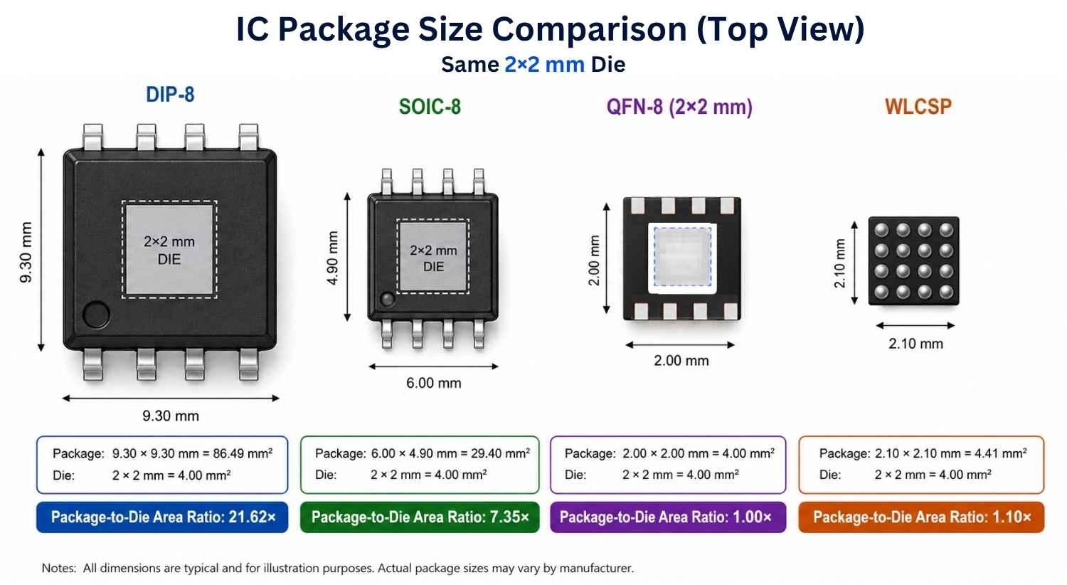
Figure: Comparison of DIP, SOIC, QFN, and WLCSP package sizes for a 2x2mm die.
| Package | Size vs Die | Typical Pitch | I/O Style |
|---|---|---|---|
| DIP | 10-20× | 2.54 mm | Through-hole leads |
| SOIC | 3-8× | 1.27 mm | Surface-mount leads |
| QFN | 1.5-3× | 0.5-0.8 mm | Perimeter pads |
| BGA | 1.5-4× | 0.8-1.27 mm | Ball array |
| CSP | ≤1.2× | 0.3-0.5 mm | Ball/bump array |
Why Chip Scale Packaging Matters in Modern Electronics
The Miniaturization Trend of Chip
PCB area per IC function has been shrinking for 20 years. A smartphone mainboard gives some ICs under 5 mm² to work with - space that a standard QFP couldn't fit into, even without any other components nearby. Chip scale packaging was the answer the industry developed: when the package is the size of the die, you stop losing board area to overhead.
While early devices used only a handful of WLPs, recent flagship smartphones such as the Apple iPhone 17 series and Samsung Galaxy S25 series integrate dozens of WLCSP and other chip-scale packages across sensors, PMICs, RF front-ends, audio codecs, wireless connectivity, and display control subsystems.
What Short Interconnect Actually Buys You
Every millimeter of conductor adds inductance. In a wire-bonded QFP, the signal path from die pad to PCB trace might span 5-8 mm. In a WLCSP, it's 150-300 µm. That difference translates directly to:
- Lower parasitic inductance → less ringing on fast digital edges
- Lower parasitic capacitance → better high-frequency signal integrity
- Reduced ground bounce → cleaner power delivery on fast load transients
- Lower switching losses → marginal but real power efficiency gains in battery-powered devices
This is why RF front-ends, PMICs, and high-speed memory controllers almost exclusively use CSP or wafer-level packaging in mobile applications.
Key Features of Chip Scale Package
| Feature | Detail |
|---|---|
| Form factor | ≤1.2× die area - smallest standard SMT package category |
| Interconnect length | 150-300 µm (die to PCB) |
| I/O style | Bottom-side solder ball or copper pillar array |
| Pitch range | 0.3 mm - 0.5 mm (most common: 0.4 mm) |
| Thermal path | Through solder balls to PCB copper; no dedicated thermal pad |
| SMT compatibility | Standard reflow profile; requires fine-pitch paste printing equipment |
Types of Chip Scale Packages
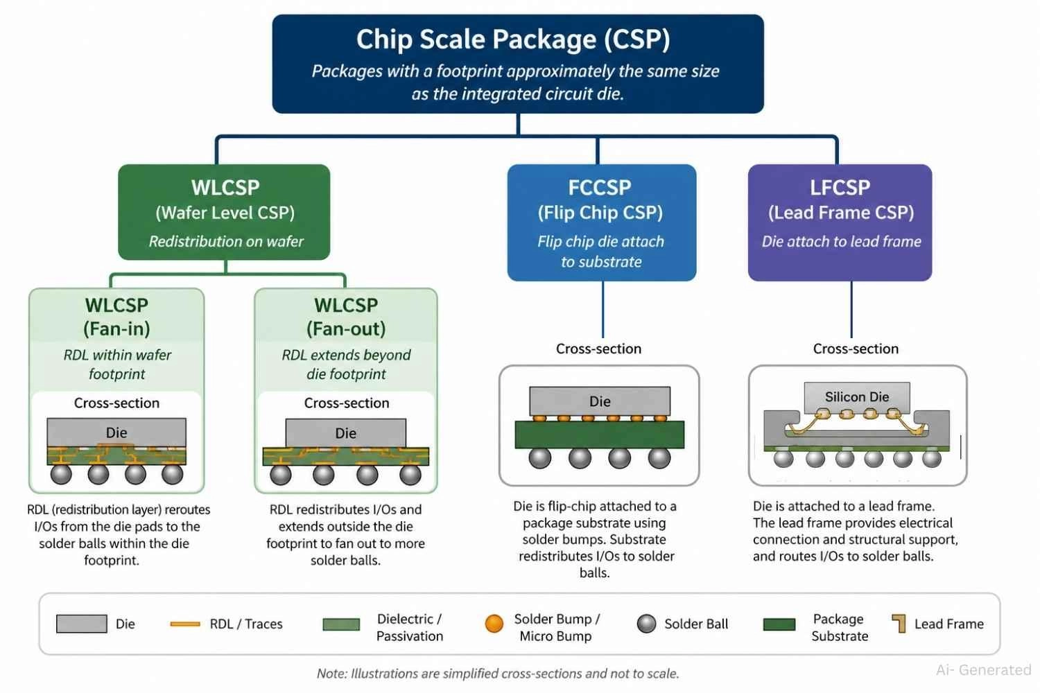
Figure: The CSP family tree including WLCSP, FCCSP, and LFCSP types.
Wafer-Level Chip Scale Package (WLCSP)
The WLCSP package is the most compact CSP variant - and the most widely used in consumer electronics. This wafer-level chip-scale package is a true chip-scale packaging technology since the resulting package is the same size as the die. It differs from other BGA package types and laminate-based CSPs in that no bond wires or interposer connections are required.
What makes WLCSP different from other CSPs: All packaging steps - redistribution, bumping, passivation - happen at the wafer level, before dicing. You process thousands of dies simultaneously rather than one at a time.
WLCSP Structure
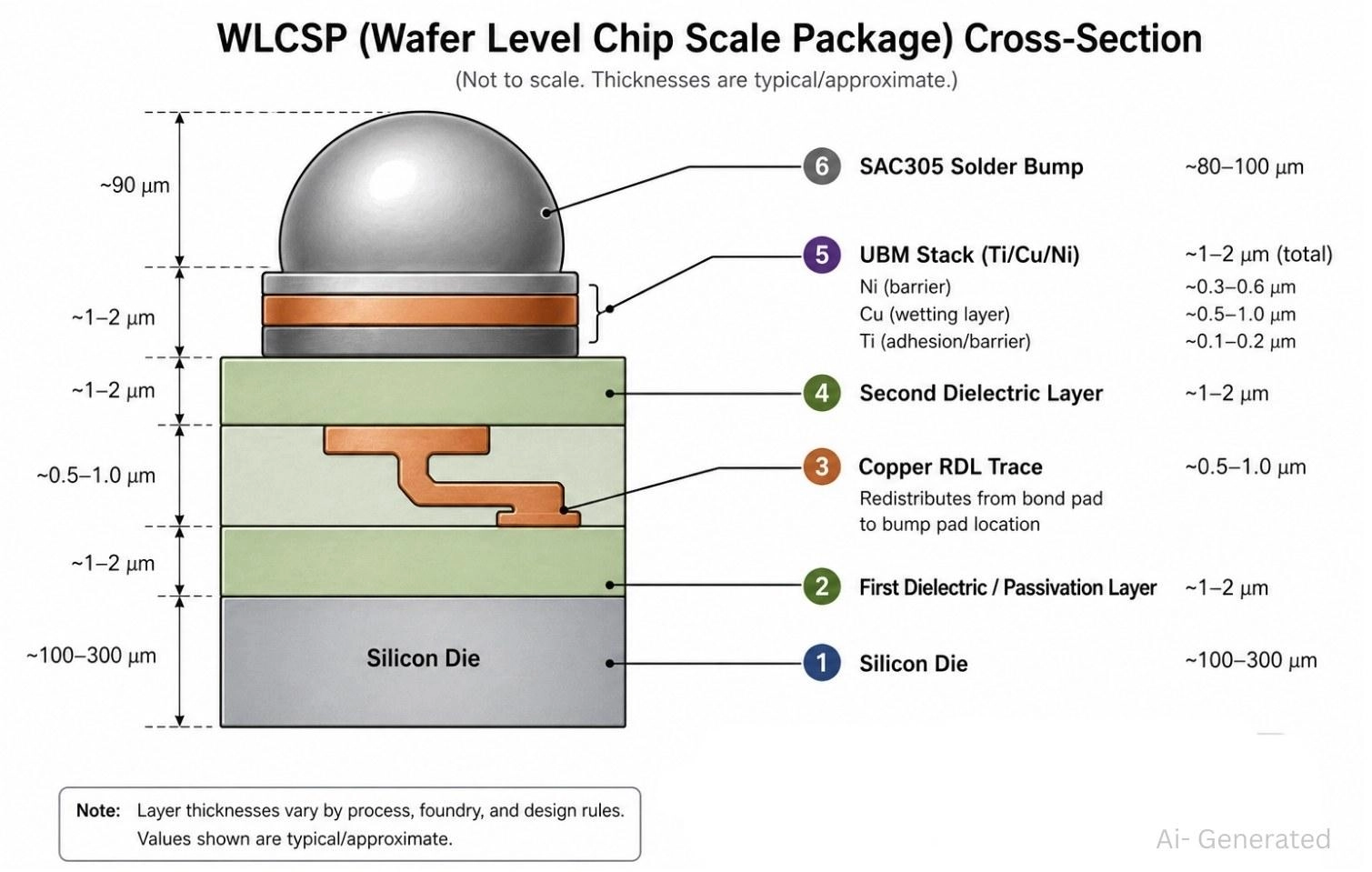
Figure: A WLCSP showing internal layers and solder bump.
The layer stack from silicon to solder ball:
- Passivation: Protects the active die surface; bond pad openings etched through
- Polymer stress buffer: Polyimide or PBO film; absorbs thermomechanical strain during thermal cycling
- Redistribution Layer (RDL): Copper traces routing from peripheral bond pads to the desired bump grid positions; single-layer RDL for simple designs, dual-layer for complex routing
- Under Bump Metallization (UBM): Ti/Cu/Ni or Ti/Cu stack; provides adhesion, diffusion barrier, and solder wettability
- Solder bumps: SAC305 alloy (96.5% Sn / 3% Ag / 0.5% Cu), 200-350 µm diameter
Quick note on cost
Because all steps happen at wafer level, cost scales with wafer area - not per-package assembly time. At high volumes with small die, WLCSP unit costs can undercut equivalent BGA or QFN options.
Flip-Chip Chip Scale Package (FCCSP)
A flip chip chip scale package (FCCSP) puts the die face-down on a thin organic substrate, with copper pillar bumps or solder bumps connecting die pads directly to the substrate routing layers below. Unlike WLCSP, there is a substrate between die and PCB solder balls.
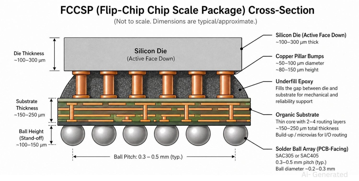
Figure: Showing FCCSP structure with die, underfill, and substrate.
- Why the substrate exists: Copper pillar pitch on modern SoC dies can be as fine as 40-100 µm. The organic substrate fans that out to 0.3-0.5 mm pitch compatible with PCB assembly. It also enables more routing layers than the thin RDL in a WLCSP.
- Why underfill matters: Silicon CTE is ~3 ppm/°C. Organic substrate CTE is ~17 ppm/°C. Without underfill, thermal cycling cracks solder joints in hundreds of cycles. Underfill epoxy distributes that thermomechanical strain across the full interface instead of concentrating it at individual bumps.
FCCSP is the go-to format for high-pin-count application processors, networking ASICs, and high-bandwidth memory controllers - anywhere WLCSP's I/O density limits become a constraint.
Leadframe Chip Scale Package (LFCSP)
A leadframe chip scale package (LFCSP) uses the same stamped copper leadframe approach as a QFN, but trims the package body down to meet the ≤1.2× die size requirement. Wire bonds connect die to leadframe; mold compound encapsulates with minimal overhang.
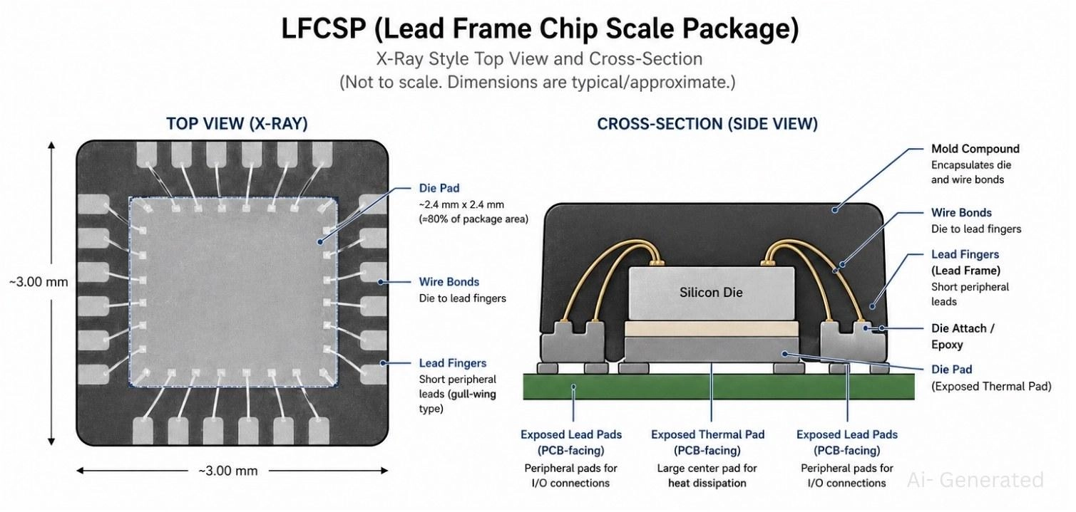
Figure: Top-view and cross-section of an LFCSP structure with wire bonds.
LFCSP vs QFN - the key differences:
| Feature | QFN | LFCSP |
|---|---|---|
| Package-to-die ratio | 2-4× | ≤1.2× |
| Molding margin | Generous | Trimmed to die edges |
| Lead count | Up to 100+ | Typically ≤32 |
| Cost | Low | Low-Medium |
| Best for | Thermal-heavy, moderate I/O | Compact, low-I/O designs |
Note
LFCSP wins on cost for simple low-I/O parts - op-amps, LDOs, sensors - where the mature wire bonding supply chain keeps unit prices competitive with no wafer-level processing overhead.
Fan-In vs Fan-Out CSP
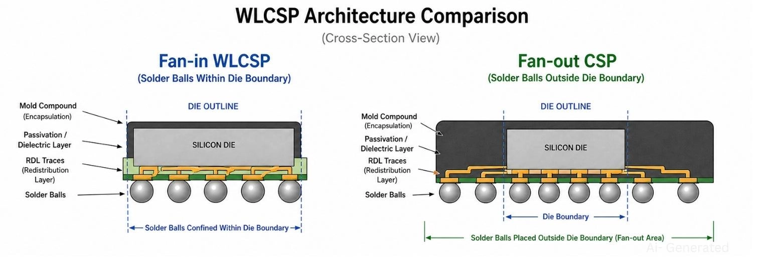
Figure: Comparison of fan-in WLCSP versus fan-out CSP.
Fan-In CSP (WLCSP is the canonical example):
- All solder balls sit within the die footprint
- I/O count limited by die area at the chosen pitch
- A 2×2 mm die at 0.4 mm pitch supports roughly 12-16 usable balls
- Lowest cost, smallest footprint
Fan-Out CSP:
- Die is embedded in a reconstituted wafer or molded panel
- RDL extends over surrounding mold compound beyond the original die edge
- Balls placed outside the die area - breaks the I/O ceiling
- Higher cost; package slightly larger than die but still very compact
- Used for high-I/O SoCs and chiplet-based designs
Chip Scale Package vs Other IC Packages
| Package | Size vs Die | Pitch | PCB Complexity | Reworkability | Best Application |
|---|---|---|---|---|---|
| DIP | 10-20× | 2.54 mm | Minimal | Easy | Prototyping, legacy |
| QFP | 4-8× | 0.4-0.8 mm | Low | Moderate | General purpose |
| QFN | 1.5-3× | 0.5-0.8 mm | Low-Medium | Moderate | Compact thermal designs |
| CSP/WLCSP | ≤1.2× | 0.3-0.5 mm | High (HDI) | Difficult | Mobile, IoT, RF |
| BGA | 1.5-4× | 0.8-1.27 mm | Medium | Difficult | High I/O SoCs |
| Bare Die (COB) | 1× | - | Very High | Very Difficult | Ultra-miniature |
Chip Scale Package vs BGA
This is the comparison engineers most often need to make. While a typical BGA package would be 7.0 mm by 7.0 mm, an equivalent WLCSP would be 2.88 mm by 3.10 mm. That's roughly 6× less board area, which is significant.
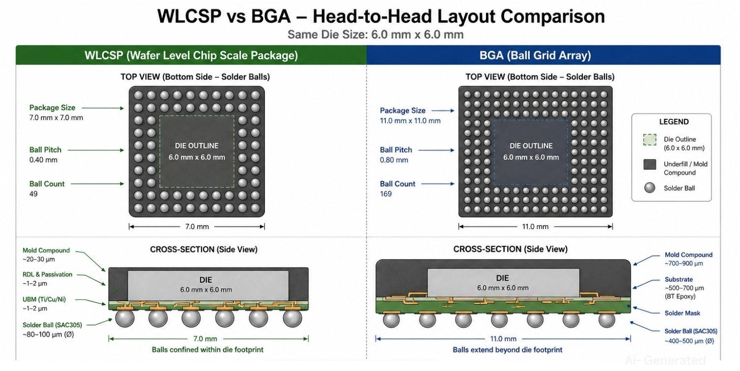
Figure: Comparison between WLCSP and BGA packages for an identical die, demonstrating the significant reduction in physical footprint.
Size and Ball Pitch
- WLCSP typically 0.3-0.5 mm pitch; package = die size
- BGA typically 0.8-1.27 mm pitch; package 1.5-4× die size
- CSP wins on board area; BGA wins on routability
Routing Complexity: At 0.8 mm BGA pitch, standard 4-layer PCBs with 100 µm trace/space can escape route most ball counts without via-in-pad. At 0.4 mm WLCSP pitch, you typically need:
- ≤75 µm trace/space
- Laser-drilled microvias
- Via-in-pad (VIPPO) for any package with more than 2 rows
That moves the PCB into HDI territory - and adds cost. The package is cheaper; the board is more expensive. Evaluate system cost, not just package cost.
When to Choose CSP vs BGA
| Choose CSP when... | Choose BGA when... |
|---|---|
| Board area is the primary constraint | I/O count exceeds ~100 |
| I/O count is moderate (4-120) | PCB routability must stay simple |
| Low parasitic inductance is critical | Reworkability in production matters |
| Power dissipation is under ~500 mW | Die is large and BGA overhead is acceptable |
Chip Scale Package vs QFN
- Thermal: QFN's exposed center thermal pad is a dedicated low-resistance heat path. For parts dissipating over 1 W, that matters - WLCSP distributes heat across all solder balls with no single thermal pad, which works for low-power ICs but becomes limiting above ~500 mW.
- Assembly: QFN at 0.5-0.8 mm pitch is within reach of most standard SMT lines. WLCSP at 0.3-0.4 mm pitch requires finer stencils and tighter placement alignment.
- Electrical: CSP wins - shorter interconnect, lower parasitics.
- Rule of thumb: 200 mW Bluetooth SoC → CSP. 2 W motor driver → QFN.
CSP vs WLP - Clearing Up the Confusion
These terms overlap and cause real confusion. Here's the distinction:
- WLP (Wafer-Level Package) = a manufacturing process - packaging steps happen at wafer level
- CSP (Chip Scale Package) = a size specification - package is ≤1.2× die size
- WLCSP = both: wafer-level processed AND chip-scale in size
All WLCSPs are CSPs. Not all CSPs are WLCSPs - FCCSP and LFCSP also meet the size spec but use substrate or leadframe processes.
How to Choose the Right IC Package
When to choose CSP:
- Board area is your hardest constraint
- I/O count is 4-120 (fan-in WLCSP); higher with fan-out
- The design is RF, high-speed analog, or requires low parasitic inductance
- Power dissipation is under ~500 mW (WLCSP) or ~2 W (FCCSP with thermal design)
- Your PCB fabrication partner supports HDI
When NOT to use CSP:
- Your PCB budget requires standard 2-layer or low-cost fab
- I/O count is 200+
- Power dissipation is high and a dedicated thermal pad is needed
- Board-level rework is part of your production or field return process
- The design must survive aggressive drop or vibration testing without underfill
| Factor | CSP | BGA | QFN |
|---|---|---|---|
| Board area | Best | Moderate | Moderate |
| Electrical performance | Excellent | Good | Good |
| Thermal dissipation | Moderate | Moderate | Best |
| PCB complexity | High | Medium | Low |
| Reworkability | Hard | Hard | Moderate |
| Package cost | Medium | Medium-High | Low |
| High I/O count | Limited | Excellent | Limited |
Note
Thermal dissipation depends heavily on PCB copper design and the specific CSP package technology used.
Advantages of Chip Scale Package
- 20-80% smaller PCB footprint than traditional packages for the same die.
- 10-20× lower parasitic inductance vs wire-bonded packages - critical for RF and fast digital designs.
- Lower EMI and better RF behavior - A CSP IC package minimizes antenna effects and crosstalk due to ultra-short routing.
- Reduced package inductance - The direct bump-to-pad connection ensures rapid switching without power integrity drops.
- Better signal integrity - less ground bounce, lower SSN, reduced noise coupling in mixed-signal designs.
- Scale economics - WLCSP cost scales with wafer area; at high volumes with small die, unit cost undercuts BGA equivalents.
- Known Good Die - Wafer-level electrical test before dicing reduces PCB assembly yield losses from bad dies.
Disadvantages and Challenges of Chip Scale Package
- Difficult Rework: Fine pitch and bottom-side I/O require specialized equipment for every rework attempt, including X-ray verification and precise thermal profiling. Plan for this cost explicitly if frequent repair is needed.
- Sensitive Assembly: Eliminating the leadframe and mold compound makes WLCSP a fragile package. It requires careful handling and pick-and-place machines with compliant nozzle tips and precise Z-height control.
- Requires HDI PCB: Fine pitch forces the use of sub-75 µm traces, laser-drilled microvias, and via-in-pad. This necessitates advanced HDI PCB design techniques, adding fabrication cost and lead time.
- Thermal Cycling Reliability: CTE mismatch between silicon (~3 ppm/°C) and FR4 PCB (~17 ppm/°C) concentrates stress at the solder joints. For rigorous automotive or industrial applications, FCCSP with underfill is often required.
- I/O Ceiling on Fan-In: A 2×2 mm WLCSP at 0.4 mm pitch holds roughly 12-16 usable balls. Increasing I/O requires a larger die area or fan-out processing, both of which add cost.
Design Considerations for Chip Scale Package
PCB Layout and Escape Routing
Getting signals out from under a WLCSP is the hardest routing task on most CSP boards. Three approaches:
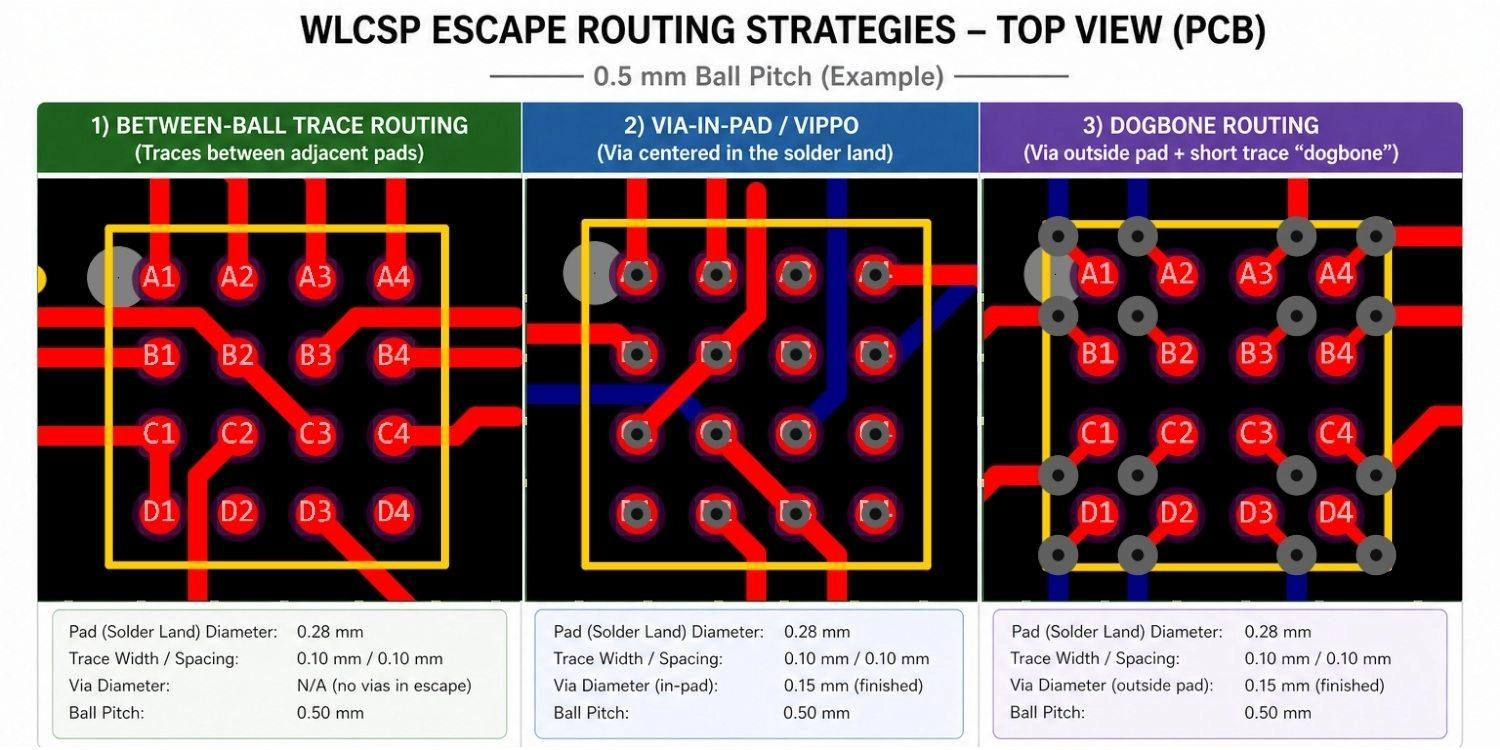
Figure: Comparing three WLCSP escape routing strategies: between-ball, via-in-pad, and dogbone.
| Strategy | When to Use | Limitation |
|---|---|---|
| Between-ball trace routing | ≥0.5 mm pitch, outer rows only | Not possible at 0.3-0.4 mm |
| Via-in-pad (VIPPO) | Fine pitch, inner rows | Adds PCB cost; must be filled and capped |
| Dogbone routing | Moderate pitch with space available | Needs clearance outside the pad |
For packages with more than 2 ball rows, VIPPO is typically unavoidable for inner rows.
Pad and Solder Mask Rules
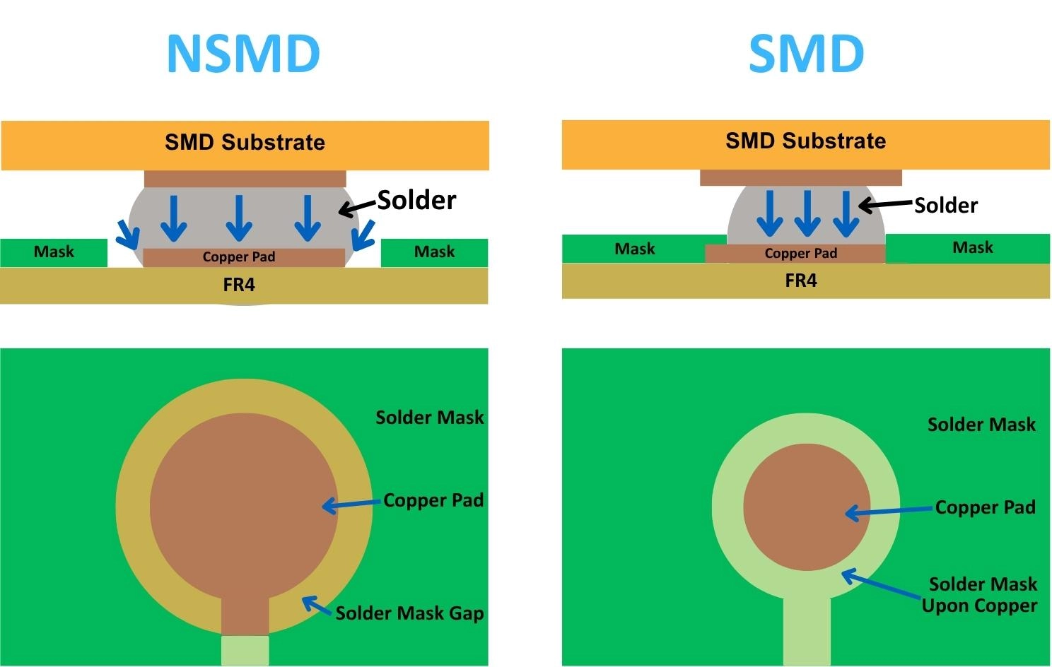
Figure: Comparison of NSMD and SMD pad designs for solder joints
- NSMD vs. SMD: Use NSMD pads for thermal fatigue reliability (the standard for consumer/IoT), as solder wets the pad sides for a stronger joint. Use SMD pads only if drop test performance is the primary concern.
- Solder Mask Webbing: At 0.3-0.4 mm pitch, webbing is extremely thin (50-75 µm). Use Liquid Photoimageable (LPI) solder mask and confirm your PCB fab's registration tolerance to prevent mask shifting and solder bridging.
Via-in-Pad (VIPPO)
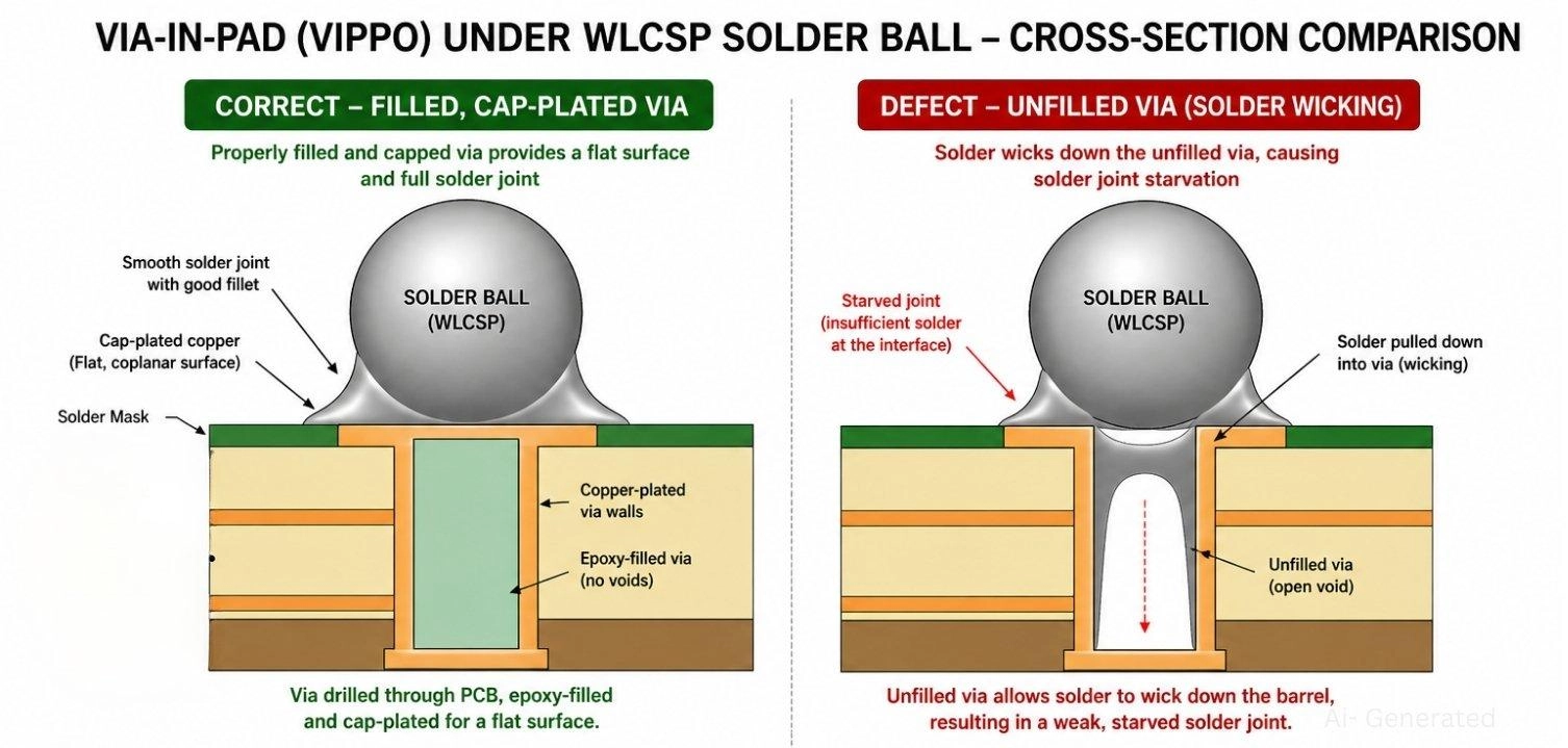
Figure: Correct via-in-pad (VIPPO) structure compared to a defective unfilled via.
Unfilled vias trap flux and starve the solder joint above. If using via-in-pad, the VIPPO (Via-in-Pad, Plated Over) process is non-negotiable for reliability. This requires drilling, plating, epoxy-filling, and cap-plating the via perfectly flat before surface finish.
Thermal Management
WLCSPs lack dedicated thermal pads, making them entirely PCB-driven. Maximize copper pour under the component, stitch thermal vias to inner planes, and use 4-layer PCBs to effectively reduce θ_JA.
CSP Assembly Process Explained
Solder Paste Printing
Stencil design is critical and non-negotiable at fine pitch, and the standard SMT assembly process equipment requires specific tuning. Key parameters from manufacturer application notes:
- Solder Paste Printing: Requires a 75-100 µm thick stencil (laser-cut stainless steel) with specific square apertures. Use Type 4 or finer solder paste.
- Pick and Place: Demands automated fine-pitch machines with vision alignment (no mechanical centering). Use compliant nozzle tips and Z-height control to avoid bump damage.
- Reflow: Follow a standard reflow soldering profile (SAC305 lead-free) keeping the ramp rate below 3°C/sec to prevent thermal shock to the silicon.
- Inspection: Because joints are hidden beneath the die, 2D X-ray is mandatory to detect bridging and voids, while 3D CT X-ray is used for precise volumetric inspection.
Reliability Testing (JEDEC Standards)
| Test | Standard | Condition |
|---|---|---|
| Temperature Cycling | JESD22-A104 | -40°C to +125°C, 1000 cycles (consumer); 2000 cycles (automotive) |
| Drop Test | JESD22-B111 | Critical for wearables and handheld devices |
| Moisture Sensitivity | J-STD-020 | Typically MSL 1 or MSL 2 |
| Bend Test | IPC-9702 | Board-level mechanical stress |
Applications of Chip Scale Package
1. Smartphones: Every flagship phone PCB is dense with CSP package technology. Power management ICs, RF transceivers, and audio codecs are all wafer-level packaged, as the size constraint is absolute for modern 6-8 mm thin devices.
2. Wearables: With usable board areas often under 20 cm², devices require the smallest available footprint, meaning a WLCSP package is used for virtually every IC in a competitive wearable design.
3. IoT Devices: Cost and size compete equally. WLCSP variants reduce module area while keeping component BOM costs highly competitive, and their lower parasitic losses extend battery life.
4. Medical Electronics: Implantable devices require sub-centimeter form factors with additional hermetic sealing for multi-year reliability.
5. Automotive Electronics: Used in ADAS and infotainment (AEC-Q006 qualified), though often less preferred in high-heat or high-stress industrial environments compared to space-constrained consumer applications.
6. CSP LED Packaging: The LED die is packaged with phosphor applied directly to die surfaces and solder bumps on the bottom (no leadframe), offering higher luminous efficacy and a superior thermal path directly to the PCB.
From Design to Production: Reliable CSP Assembly with JLCPCB
Getting a WLCSP design from schematic to assembled board involves more process discipline than standard SMT. Most early CSP failures in production come from insufficient PCB capability or lack of X-ray inspection - not the design itself.
Challenges Engineers Face with CSP Manufacturing
Two common failure modes catch engineers in their first build:
1. Fine-pitch paste printing failures - A paste printer running at ±50 µm registration accuracy struggles to hit ±25 µm demanded by 0.4 mm WLCSP pitch consistently across a full panel. The result: insufficient paste on edge balls, bridging on inner balls, or inconsistent deposit volumes that cause cold joints after reflow.
2. Hidden joint defects - Every solder joint under a WLCSP is invisible to AOI. Without X-ray inspection, voids, inner-row cold joints, and subtle bridging pass through functional test and fail in the field.
How JLCPCB Simplifies CSP-Based PCB Assembly
JLCPCB's PCB assembly service addresses both directly:
- Fine-pitch SMT capability - Placement equipment handles 0.3 mm pitch components with vision-alignment feedback, not mechanical centering.
- Stencil engineering - For WLCSP designs, aperture geometry is matched to the specific part pitch and pad type before paste printing begins.
- X-ray inspection - Standard for fine-pitch ball grid components; not an optional add-on.
- DFM review - Gerber files are checked against component specs before manufacturing starts - VIPPO requirements, solder mask web violations, and stencil aperture mismatches flagged on paper rather than in hardware.
Future Trends in Chip Scale Packaging
Fan-Out Wafer-Level Packaging (FOWLP)
TSMC's InFO, ASE's FOCoS, and Samsung's FO-WLP are all production FOWLP platforms. The next evolution: multi-die FOWLP embedding heterogeneous dies in a single reconstituted wafer with inter-die RDL routing - the foundation of chiplet architectures for AI and 5G applications.
3D IC and TSV Stacking
Through-Silicon Vias enable vertical die stacking with electrical connections through the silicon. HBM (High Bandwidth Memory) is the most mature application - stacking 4-12 DRAM dies with 55 µm TSV pitch. Hybrid bonding (sub-10 µm pitch, copper-to-copper direct bond) is the next step for AI accelerator memory integration.
Heterogeneous Integration
The chiplet model - multiple specialized dies in one package - is moving down-market. Mixed-signal chiplets, integrated passive components, and RF front-end integration within CSP-format modules are in active development across TSMC, Intel, and the OSAT ecosystem.
AI and HPC Packaging
AI accelerators need enormous memory bandwidth at low latency. CoWoS (Chip-on-Wafer-on-Substrate), EMIB, and 3D-stacked die architectures are the current high-end solutions. Over the next decade, the interconnect density and thermal management techniques developed for AI packaging will propagate into mainstream CSP formats.
FAQs About Chip Scale Package
Q: Does a wafer-level chip scale package (WLCSP) require underfill?
Standard fan-in WLCSP packages used in consumer electronics usually do not require underfill, as the polymer stress buffer layer absorbs thermomechanical strain. However, for flip chip chip scale packages (FCCSP) or applications in extreme automotive environments, underfill epoxy is often necessary to prevent solder joint cracking from CTE mismatch.
Q: What type of solder paste is recommended for CSP package assembly?
Due to the fine pitch (0.3 mm-0.5 mm) of a CSP package, standard Type 3 solder paste is inadequate. Engineers should specify Type 4 (or even Type 5) no-clean solder paste, which features smaller solder spheres (25-36 µm) to ensure clean release from the fine stencil apertures and prevent bridging.
Q: Are chip-scale packages more expensive than traditional BGA or QFN?
At the component level, wafer-level packaging can actually be cheaper in high volumes because the packaging steps are applied to the entire wafer at once. However, the total system cost may increase because a chip-scale package often forces the use of more expensive HDI PCB fabrication and specialized fine-pitch assembly processes.
Q: How do I test or prototype with a chip-scale package?
Bare CSPs cannot be easily hand-soldered or probed with standard multimeter leads. For prototyping, engineers typically use breakout boards (adapters that convert the fine-pitch array to standard 2.54 mm headers) or rely on turnkey PCBA services like JLCPCB to machine-assemble the initial test boards.
Q: Where is the chip-scale package LED used?
SP LEDs are used in automotive headlamp modules, mini-LED backlights for display panels, high-power illumination fixtures, and any application requiring a small light-emitting point source with efficient heat dissipation and high luminous efficacy.
Conclusion
Chip scale packaging solves one problem - the package taking up space the silicon doesn't need - and delivers a cascade of benefits: smaller boards, shorter signal paths, lower parasitics, and, in high volumes, competitive unit costs. As electronics continue to shrink, mastering the chip-scale package (CSP) layout constraints will only become more critical for engineers. The shift toward advanced chip-scale packaging will continue to define the next generation of hardware.
For WLCSP and fine-pitch designs, JLCPCB offers full-stack fabrication and PCB assembly - including HDI with VIPPO, precision SMT, and standard X-ray inspection. Start with a free DFM review to catch errors early and avoid costly respins. Quote your design today.
Popular Articles
• Common PCB Assembly Methods and Soldering Techniques Explained
• What Is BGA Void? Causes, IPC Limits, and Solutions
• SMD Soldering Tools You Need: Complete Guide from Beginner to Pro
• Reflow Soldering: Everything You Need to Know
• SMT Assembly Process Explained and Equipment Used: A Step-by-Step Guide to PCBA Manufacturing
Keep Learning
12 Professional Soldering Tips and Tricks Every Beginner Should Know
Soldering is not merely "gluing" metal; it is a metallurgical process that creates an intermetallic compound (IMC). This molecular bond ensures the electrical and mechanical integrity of your device. A poor joint might pass a quick visual check but will inevitably fail under vibration or thermal stress, leading to "ghost" bugs and hardware failures. These soldering tips and tricks focus on practical, repeatable techniques used in professional electronics soldering—from correct heat transfer and flux u......
Solder Melting Point Guide: Chart, Alloy Types, and Reflow Considerations
In the precise world of electronics manufacturing, a difference of just a few degrees can mean the distinction between a perfect, reliable solder joint and a catastrophic "cold" joint failure. While many hobbyists view soldering simply as "melting metal to stick things together," professional PCB assembly requires a nuanced understanding of thermodynamics. The solder melting point is not simply a single value listed in a datasheet; it is a decisive limit that determines the choice of components, the s......
The Ultimate Guide to Solder Flux: Everything You Should Know Before Soldering PCB
Soldering is needed to make almost all electronic devices. Adding solder alone won't make a joint that is strong, clean, and sound from a metallurgical point of view. Solder flux is a very important part of the process that comes in here. If you want to do your job better and make it more reliable, you need to know a lot about soldering flux, whether you're an engineer, a professional technician, or just a hobbyist. This article goes into a lot of detail about solder flux, including what it is, how it......
Common PCB Assembly Methods and Soldering Techniques Explained
Whether you're designing your first prototype or scaling up to production, understanding PCB assembly methods and soldering techniques is crucial to achieving reliable, high-performance circuit boards. Modern PCBA primarily relies on Surface Mount Technology (SMT) and Through-Hole Technology (THT)—each offering unique advantages for component density, durability, and manufacturability. In this guide, we'll break down the major PCB assembly methods, key soldering techniques such as reflow and wave sold......
Flex PCB Assembly Guide: Process, Challenges, and Solutions
Flexible Printed Circuit Boards (Flex PCBs) are the foundational technology enabling the compact, innovative design of modern electronics. Because of their ability to bend and fold, they power devices from smart wearables to compact medical instruments where traditional rigid printed circuit boards (Rigid PCBs) can't be used. Achieving a functional electronic circuit from the raw plastic film demands special expertise, with flexible PCB assembly (FPCA) representing the crucial final step in this trans......
SMD Rework Guide: Tools, Temperatures, and Techniques That Prevent PCB Damage
From replacing a burned regulator to correcting wrong component values or removing solder bridges on fine-pitch ICs, SMD rework is an essential skill in electronics manufacturing and prototyping. It allows engineers to repair assembly defects, implement design changes, and recover valuable PCBs without the cost and delay of building new boards. In this guide, you will learn: What SMD rework is Common rework scenarios Tools and temperatures Safe removal and installation Package-specific techniques Real......