
The Ultimate Guide to Solder Bridging — What It Is, What Causes It & How to Fix It
13 min
- What Is Solder Bridging?
- Why Does Solder Bridging Occur?
- How to Detect Solder Bridging
- How to Fix Solder Bridges
- The Risks of Solder Bridging
- How to Prevent Solder Bridging
- How JLCPCB Minimizes Solder Bridging Through Reliable PCB Fabrication & Assembly
- FAQ
- Conclusion
As modern electronics continue to shrink - moving from 0805 passives to microscopic 0201s and high-density Ball Grid Arrays (BGAs) - the margin for error in PCB assembly (PCBA) vanishes. In this precision environment, even a microscopic amount of excess alloy can lead to one of the most frustrating defects in manufacturing: solder bridging.
For engineers and hobbyists alike, a solder bridge is more than just a cosmetic flaw; it is a critical failure that can ruin components and delay production. While Design for Manufacturing (DFM) guidelines help, partnering with a high-precision manufacturer like JLCPCB PCBA service is the first line of defense.
In this guide, we will analyze the root causes of solder bridging, how to detect it using professional methods, and the specific steps to fix and prevent it.
What Is Solder Bridging?
In technical terms, what is solder bridging? It is an unintended electrical connection between two conductive leads or pads that should be isolated. Ideally, solder should adhere only to the metal pad and the component lead, separated by the non-conductive solder mask. When the solder spreads across the mask and joins two adjacent points, a bridge is formed.
It is important to distinguish between a solder bridging defect and an intentional design feature. Engineers often design a solder bridge jumper - a specific footprint consisting of two close pads intended to be bridged manually to configure board settings. However, when this happens accidentally on the fine-pitch pins of a microcontroller, it is a critical defect.
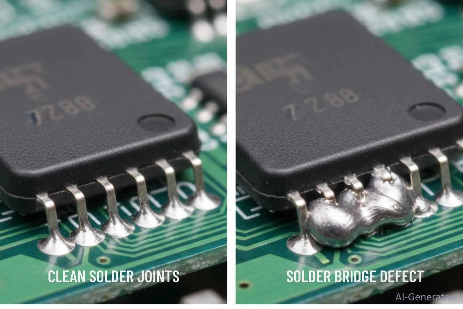
Figure: Comparison showing clean SMT solder joints versus a solder bridging defect on a microprocessor.
How Solder Bridges Affect PCB Functionality
The most immediate impact of a solder bridge is a short circuit. If a bridge connects a power line (VCC) to a ground line (GND), the best-case scenario is that the device simply won't power on. The worst-case scenario is catastrophic thermal failure - traces burning, batteries venting, or sensitive ICs being destroyed instantly.
Even "micro-bridges" that are barely visible pose a reliability risk. They may pass a quick continuity check, but can eventually cause intermittent signal failures due to electromigration or thermal expansion during device operation.
Why Does Solder Bridging Occur?
A solder bridge in PCB assembly is rarely caused by bad luck. It is usually the result of specific process variables drifting out of spec.
#1 Excess Solder Leading to Bridges
The most common solder bridge cause is the application of too much solder paste. In the Surface Mount Technology (SMT) process, a stencil is used to print paste onto pads. If the stencil aperture (the hole size) is too large relative to the pad - for example, a 1:1 ratio on a 0.4mm pitch component - the excess paste has nowhere to go during reflow and will spill over to the adjacent pad.
#2 PCB Design Issues (Pad Spacing & Solder Mask)
Sometimes the issue is baked into the Gerber files. If the solder bridge footprint design violates minimum clearance rules, bridging is inevitable.
● Insufficient Solder Mask Dams: The "dam" is the thin strip of green mask between pads. If this dam is narrower than 4 mil (0.1mm), it may peel off during manufacturing or fail to repel the molten solder.
● Solder Mask Slivers: Thin slivers of mask can detach and float into the molten solder, creating a pathway for a bridge to form.
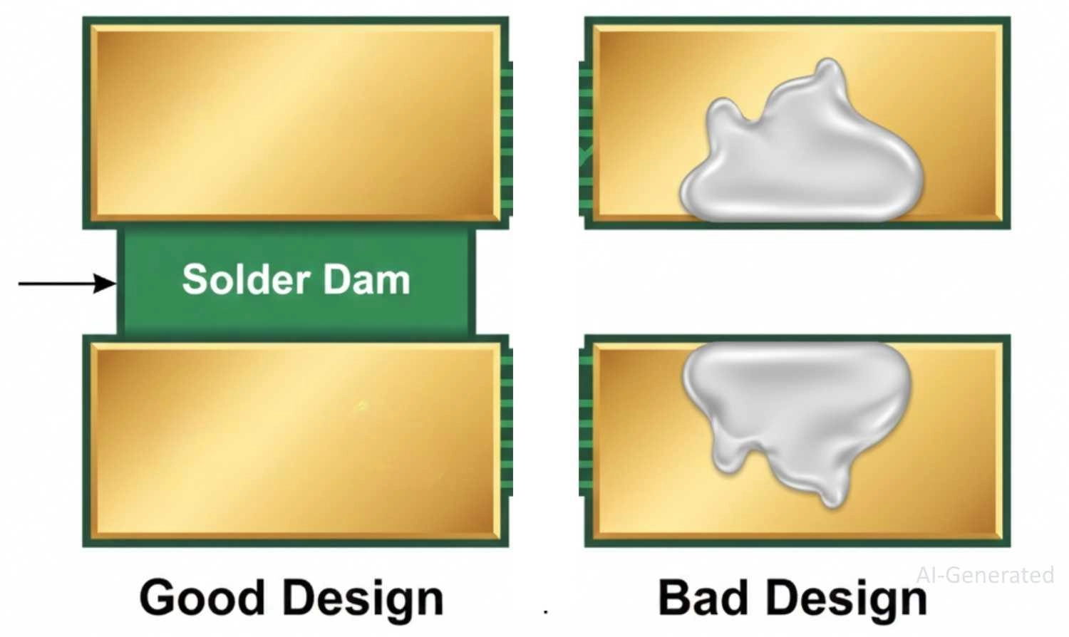
Figure: Solder mask dams preventing solder flow between PCB pads.
#3 Incorrect Soldering Temperature & Reflow Profile
Soldering relies on surface tension. If the reflow profile is incorrect, this tension fails:
● Ramp-Up Too Fast: Flux activates explosively, causing paste to splatter and bridge.
● Peak Temp Too Low: The solder doesn't reach the liquidus state long enough to "wet" properly. Good wetting pulls the solder back onto the pad; poor wetting leaves it slumped between pads.
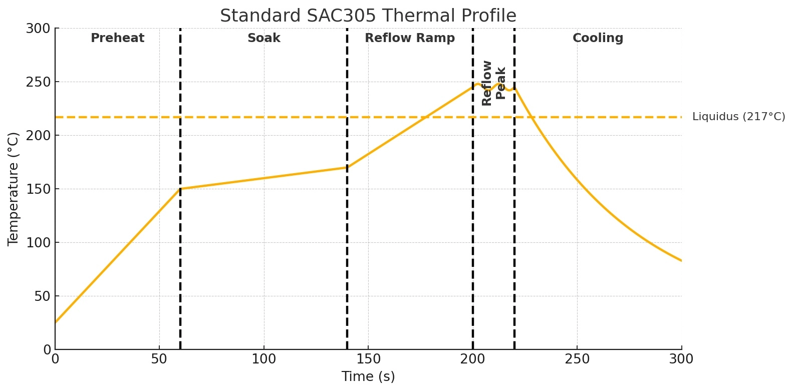
Figure: Standard SMT Reflow Profile graph highlighting the importance of the soak zone for flux activation.
#4 Causes in Wave Soldering (Pin Length & Conveyor Angle)
While SMT gets the most attention, bridging is the #1 defect in through-hole wave soldering.
● Pin Length: If component leads stick out too far (e.g., >2mm) beneath the board, they drag in the molten wave, pulling solder with them and bridging to neighbors.
● Conveyor Issues: If the speed is too fast or the angle is too shallow, the excess solder doesn't have time to drain back into the pot before solidifying.
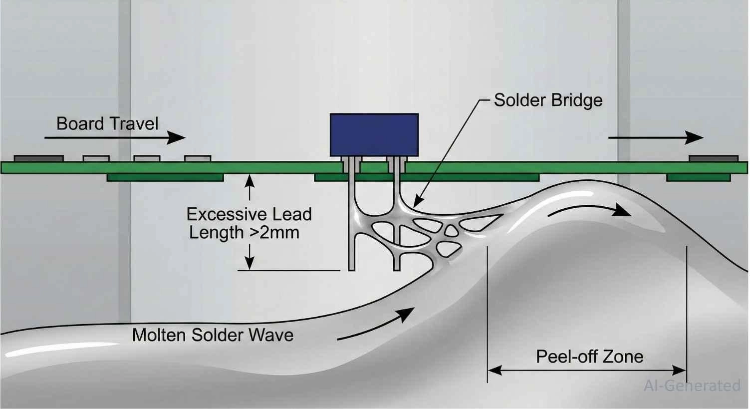
Figure: Showing how excessive component lead length causes solder bridging during wave soldering.
#5 Misaligned Components or Stencils
Precision is key. If the pick-and-place machine shifts a component by just 0.1mm, the leads might land on the edge of the pads. During reflow, as the component settles, the displaced paste can squeeze out and bridge.
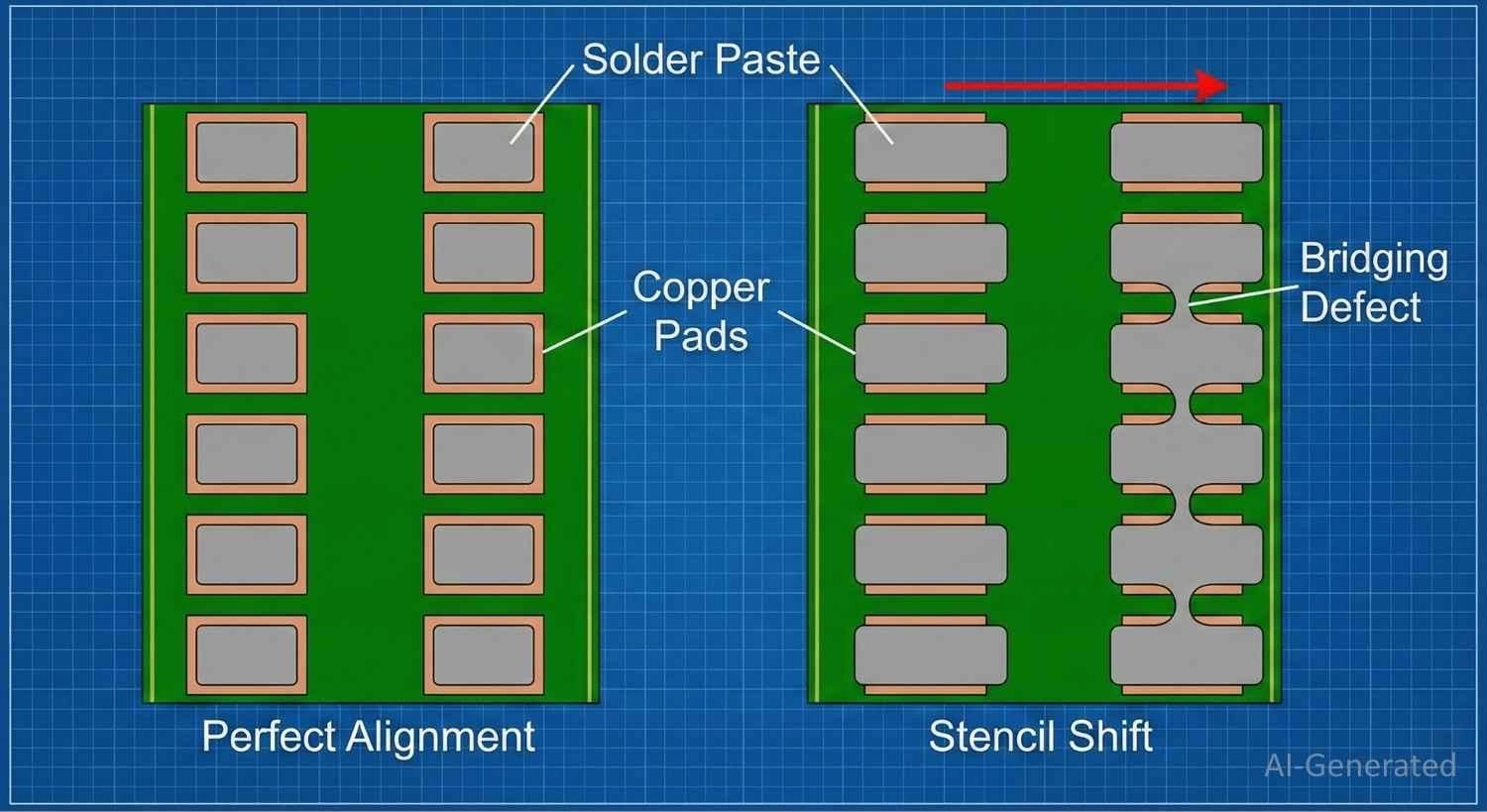
Figure: Showing how stencil misalignment causes solder paste to be printed between pads, leading to bridges.
#6 Contaminated Surfaces or Poor Solder Paste Quality
Old solder paste (where the flux has dried out) or oxidized PCB pads (poor surface finish) prevent smooth flow. Instead of coating the metal, the solder balls up and rolls into the gaps between pins.
How to Detect Solder Bridging
#1 Visual Inspection with Magnification
For leaded components (like QFPs and SOPs) and passives, visual inspection is the first step. Technicians use Mantis stereo microscopes or digital magnifiers to look for the tell-tale reflective glint of solder between pins.
#2 Using a Multimeter for Continuity Testing
If a bridge is suspected but not visible (e.g., hidden under a connector body), a multimeter is essential.
1. Set the multimeter to Continuity Mode (beep).
2. Consult the schematic to identify the solder bridge symbol or intended connections.
3. Probe adjacent pins. A beep indicates a short. Always verify with the schematic, as some adjacent pins (like multiple GND pins) are connected intentionally.
#3 Automated Optical Inspection (AOI) for SMT Production
At JLCPCB, we don't rely on human eyes alone. AOI machines scan every assembled board using high-resolution cameras and various light angles. The software analyzes the shape and reflection of every joint. If a joint appears continuous with its neighbor, the AOI flags it as a defect.
#4 X-Ray Inspection (AXI) for BGA Components
For BGAs, where the solder joints are sandwiched between the component and the board, visual inspection is impossible. Automated X-ray Inspection (AXI) is required. X-rays can see through the silicon and plastic, revealing if the solder balls underneath have merged into a bridge.
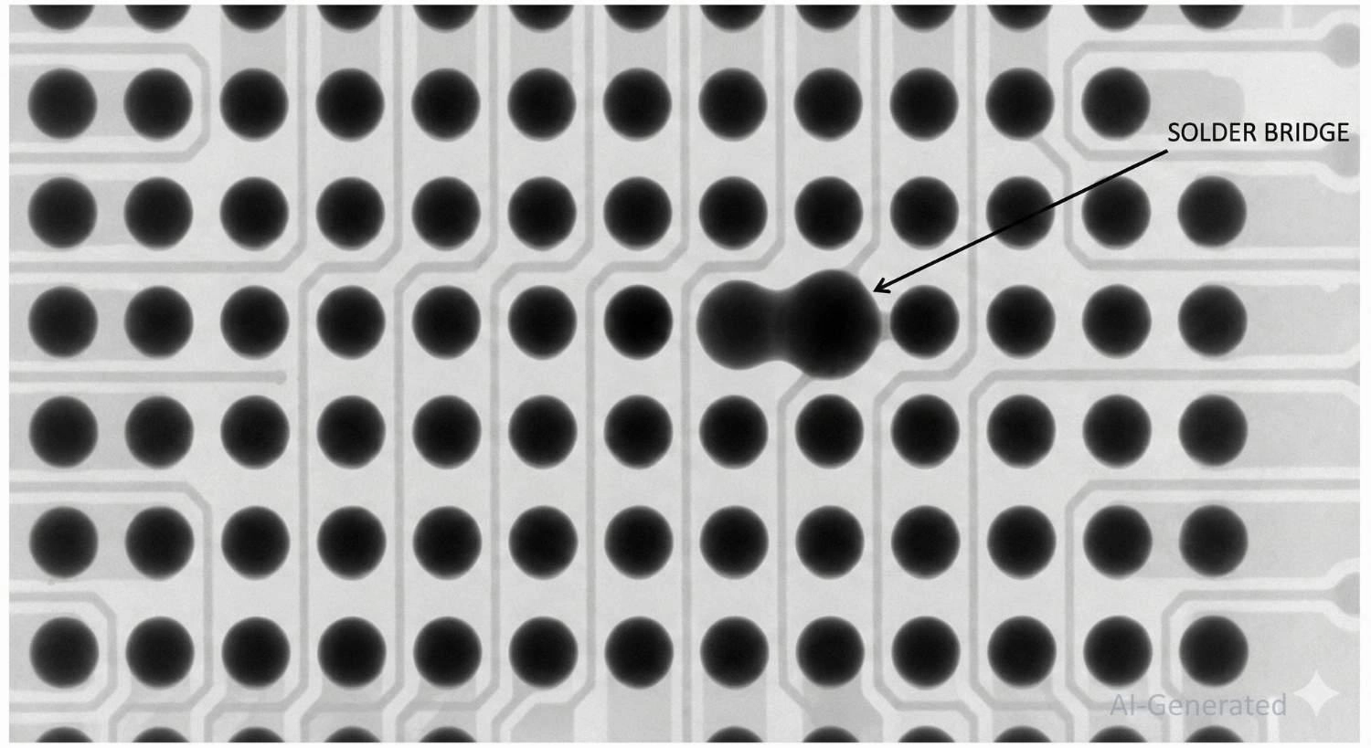
Figure: X-ray inspection image revealing a hidden solder bridge defect under a BGA component.
How to Fix Solder Bridges
#1 Using Solder Wick / Desoldering Braid
This is the standard method for how to remove solder bridge defects.
1. Apply a small amount of liquid or gel flux to the bridge.
2. Place the copper desoldering braid (wick) over the bridge.
3. Press a hot soldering iron onto the braid.
4. Wait a few seconds for the heat to transfer; the braid will suck up the molten solder via capillary action.
5. Lift the iron and braid together to avoid sticking.
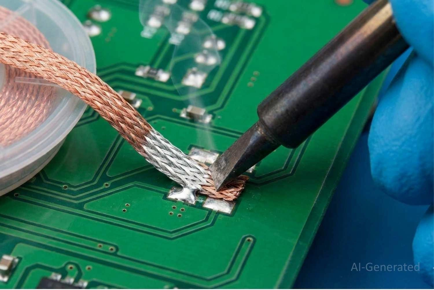
Figure: Using copper desoldering wick to absorb excess solder and fix a bridge.
#2 Hot Air Gun and Drag Solder Techniques
For multi-pin ICs, the "drag solder" technique is effective for how to fix solder bridge issues without removing all the solder.
1. Flood the pins with flux.
2. Use a clean, hoof-tip soldering iron or hot air.
3. Drag the iron across the pins. The surface tension of the molten solder, aided by the flux, will cause it to snap back onto the pads and break the bridge.
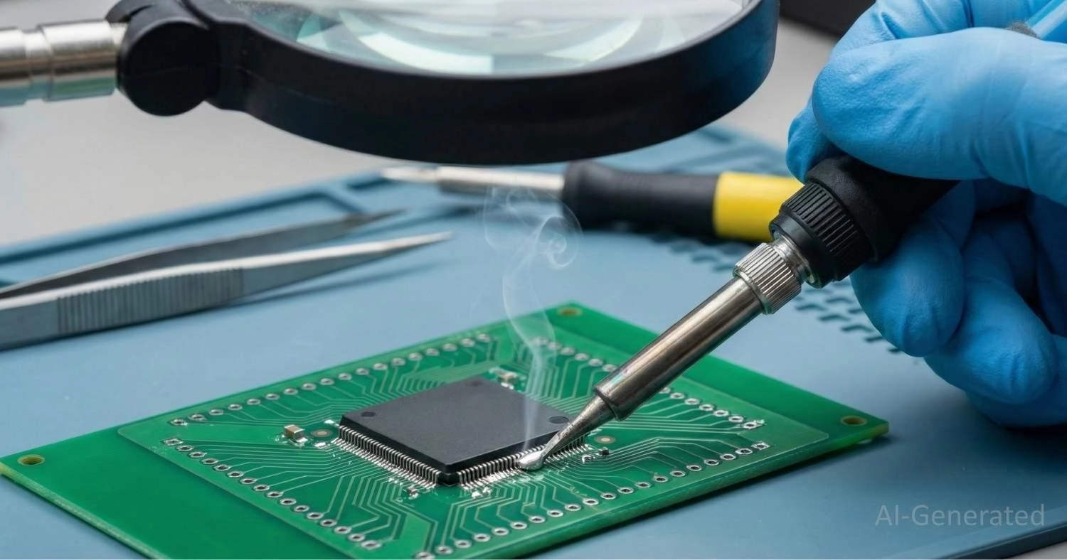
Figure: Technician performing the drag soldering technique to clear solder bridges on a fine-pitch IC.
#3 Mechanical Removal (For Prototypes Only)
In rare cases on prototype boards, a technician might use a heated knife tip to "slice" a bridge while the solder is molten.
Warning: This is risky. One slip can cut a trace or lift a pad. This method is never used in professional production, but it can save a prototype in a pinch.
#4 Expert Tips from Forums & Communities
● Flux is your friend: Most bridging issues are actually "lack of flux" issues. Flux helps solder flow where it belongs.
● Don't Overheat: Applying heat for too long can delaminate the copper pad from the fiberglass (FR4), ruining the board permanently.
The Risks of Solder Bridging
1. Electrical Short Circuits & Device Failure
Shorts are the primary danger. In high-power circuits, a bridge can cause arcing. In data lines, it can cause signal corruption that is incredibly difficult to debug because the device appears "alive" but behaves erratically.
2. Impact on High-Density PCB Designs
As designs move toward high-density interconnects (HDI), repairing a bridge becomes exponentially harder. A bridge under a CSP (Chip Scale Package) is physically inaccessible to a soldering iron.
3. Manufacturing Rework Costs & Yield Loss
Rework destroys efficiency. Detecting a bridge, manually desoldering it, cleaning the board, and re-inspecting it takes 10–20 minutes per board. For a production run of 1,000 units, a 5% bridging rate can add dozens of hours of labor and delay shipping.
How to Prevent Solder Bridging
Prevention is always cheaper than rework. How to prevent solder bridging relies on strict adherence to design rules and process controls.
#1 PCB Design Rules Check (Pad Spacing & Solder Mask)
Ensure your CAD layout respects the manufacturing capabilities of your fab house.
| Component Pitch | Recommended Mask Dam | Stencil Aperture Reduction |
|---|---|---|
| > 0.65mm | 0.1mm (4mil) | 0 - 10% |
| 0.5mm | 0.08mm (3-3.5mil) | 10 - 15% |
| 0.4mm | 0.05mm - 0 (Gang opening) | 20 - 25% |
#2 Use NSMD Pads for Fine-Pitch BGAs to Prevent Bridging
For fine-pitch components, using Non-Solder Mask Defined (NSMD) pads is an effective way to reduce solder bridging. In NSMD, the mask opening is larger than the copper pad, leaving a gap between the copper edge and the mask. This provides better registration and ensures the solder wraps around the copper, reducing the likelihood of bridging compared to Solder Mask Defined (SMD) pads.
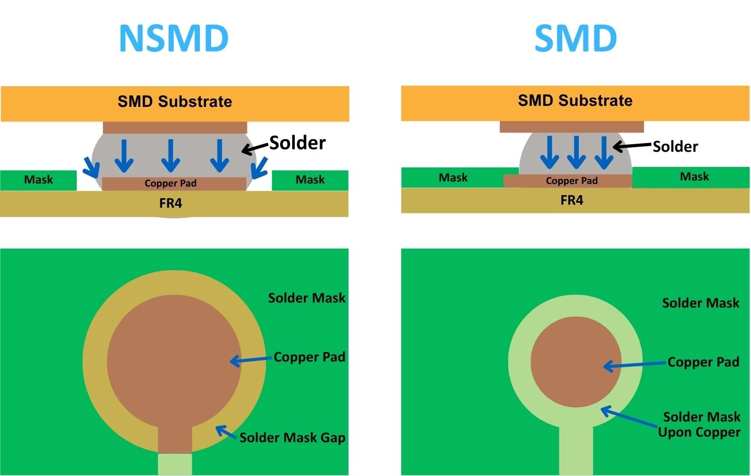
Figure: Comparison of Solder Mask Defined (SMD) vs. Non-Solder Mask Defined (NSMD) pad structures for BGA reliability.
#3 Proper Solder Paste Application in SMT
Using the right stencil is critical. For fine-pitch components, the aperture should be slightly smaller than the pad (e.g., a "home plate" or rounded square shape) to reduce paste volume. JLCPCB uses electropolished stencils, which have smoother walls, ensuring paste releases cleanly rather than sticking and smearing.
#4 Optimizing Reflow Temperature Profiles
The reflow oven must be tuned to the specific solder paste used. Extending the "Soak Zone" (the period before reflow) allows the entire board to reach a uniform temperature, ensuring that when the peak zone hits, the flux activates and cleans the pads right before the solder melts.
#5 Hand-Soldering Techniques to Avoid Excess Solder
For hobbyists, the golden rule is: Heat the pad, not the solder. Touch your iron to the junction of the pad and lead, wait a second, and then feed the solder into the joint. Feeding solder directly onto the iron creates a blob that falls onto the board, causing bridges.
#6 Surface Preparation & Cleaning
Oil, fingerprints, and dust repel solder. Always clean bare boards with Isopropyl Alcohol (IPA) before assembly. For moisture-sensitive devices, baking the board and components can prevent outgassing, which can disturb the solder joint formation.
How JLCPCB Minimizes Solder Bridging Through Reliable PCB Fabrication & Assembly
At JLCPCB, we implement industrial-grade controls to ensure your boards arrive defect-free.
1. LDI Technology: We use Laser Direct Imaging for solder mask application. This allows for extremely tight alignment, ensuring mask dams are preserved even on 0.4mm pitch ICs.
2. High-Quality Stencils: Our high-precision steel stencils ensure exact paste volume deposition.
3. 100% AOI Inspection: Every SMT order undergoes Automated Optical Inspection to catch and filter out bridging defects before they leave the factory line.

FAQ
Q1: Why does solder bridging happen more frequently on one side of a QFP chip?
This is often due to "slumping" during reflow or uneven heating. If the airflow in the oven hits one side of the chip first, that side reflows sooner. It can also be caused by a slightly warped PCB or uneven solder paste printing on that specific quadrant.
Q2: Does lead-free solder bridge more easily than leaded solder?
Yes, generally. Lead-free alloys (like SAC305) have higher surface tension and do not "wet" or spread as easily as traditional SnPb (Tin-Lead) solder. This reduced wetting action means the solder is less likely to pull back onto the pad, making it slightly more prone to bridging if process parameters aren't perfect.
Q3: Can old flux cause solder bridging?
Yes. Flux cleans oxidation to allow solder to flow. If the flux is old or expired, it loses its activity. Without active flux, the solder won't wet the pad; instead, it remains as a ball or blob that can easily roll over and bridge to an adjacent pin.
Q4: Is it better to scrap a bridged board or rework it?
It depends on the board's value. For a simple $5 IoT node, the labor cost to fix a bridge might exceed the board cost, so scrapping is better. For a complex $500 FPGA board, reworking the bridge is mandatory. However, excessive rework can degrade reliability, so the goal is always zero defects.
Q5: What is the difference between solder bridging and solder balling?
A solder bridge is a connection between two pins. Solder balling is when tiny, isolated spheres of solder scatter across the board (often on the solder mask) without necessarily connecting anything. While balls can cause shorts if they move, they are distinct defects with different causes (usually moisture or rapid pre-heating).
Conclusion
Solder bridging is a challenge inherent to the physics of soldering, but it is entirely manageable. By combining robust Design for Manufacturing (DFM) practices - like proper mask dams and aperture reduction - with precise assembly processes, you can virtually eliminate this defect. Whether you are prototyping a single board or running 10,000 units, understanding the science of wetting and flow is key to reliability.
Ready to build your next design? Trust a manufacturer that understands the details.
Get an instant quote for your PCB Assembly at JLCPCB and experience the difference high-precision manufacturing makes.

Popular Articles
• Common PCB Assembly Methods and Soldering Techniques Explained
• What Is BGA Void? Causes, IPC Limits, and Solutions
• SMD Soldering Tools You Need: Complete Guide from Beginner to Pro
• Reflow Soldering: Everything You Need to Know
• SMT Assembly Process Explained and Equipment Used: A Step-by-Step Guide to PCBA Manufacturing
Keep Learning
Common PCB Assembly Methods and Soldering Techniques Explained
Whether you're designing your first prototype or scaling up to production, understanding PCB assembly methods and soldering techniques is crucial to achieving reliable, high-performance circuit boards. Modern PCBA primarily relies on Surface Mount Technology (SMT) and Through-Hole Technology (THT)—each offering unique advantages for component density, durability, and manufacturability. In this guide, we'll break down the major PCB assembly methods, key soldering techniques such as reflow and wave sold......
12 Professional Soldering Tips and Tricks Every Beginner Should Know
Soldering is not merely "gluing" metal; it is a metallurgical process that creates an intermetallic compound (IMC). This molecular bond ensures the electrical and mechanical integrity of your device. A poor joint might pass a quick visual check but will inevitably fail under vibration or thermal stress, leading to "ghost" bugs and hardware failures. These soldering tips and tricks focus on practical, repeatable techniques used in professional electronics soldering—from correct heat transfer and flux u......
Solder Melting Point Guide: Chart, Alloy Types, and Reflow Considerations
In the precise world of electronics manufacturing, a difference of just a few degrees can mean the distinction between a perfect, reliable solder joint and a catastrophic "cold" joint failure. While many hobbyists view soldering simply as "melting metal to stick things together," professional PCB assembly requires a nuanced understanding of thermodynamics. The solder melting point is not simply a single value listed in a datasheet; it is a decisive limit that determines the choice of components, the s......
The Ultimate Guide to Solder Flux: Everything You Should Know Before Soldering PCB
Soldering is needed to make almost all electronic devices. Adding solder alone won't make a joint that is strong, clean, and sound from a metallurgical point of view. Solder flux is a very important part of the process that comes in here. If you want to do your job better and make it more reliable, you need to know a lot about soldering flux, whether you're an engineer, a professional technician, or just a hobbyist. This article goes into a lot of detail about solder flux, including what it is, how it......
Flex PCB Assembly Guide: Process, Challenges, and Solutions
Flexible Printed Circuit Boards (Flex PCBs) are the foundational technology enabling the compact, innovative design of modern electronics. Because of their ability to bend and fold, they power devices from smart wearables to compact medical instruments where traditional rigid printed circuit boards (Rigid PCBs) can't be used. Achieving a functional electronic circuit from the raw plastic film demands special expertise, with flexible PCB assembly (FPCA) representing the crucial final step in this trans......
SMD Rework Guide: Tools, Temperatures, and Techniques That Prevent PCB Damage
From replacing a burned regulator to correcting wrong component values or removing solder bridges on fine-pitch ICs, SMD rework is an essential skill in electronics manufacturing and prototyping. It allows engineers to repair assembly defects, implement design changes, and recover valuable PCBs without the cost and delay of building new boards. In this guide, you will learn: What SMD rework is Common rework scenarios Tools and temperatures Safe removal and installation Package-specific techniques Real......