
IC Package Types Explained: A Practical Guide for PCB Designers
25 min
- What Is an IC Package?
- Different Types of IC Packages: Quick Comparison
- How Many Types of IC Packages Are There?
- SMD IC Package Types: Quick Reference
- Surface Mount IC Package Types
- Through-Hole IC Package Types
- Advanced IC Packaging Types: Next-Generation Technologies
- IC Packaging in Real Projects (Practical Examples)
- How to Choose the Right IC Package for Your PCB
- Common Mistakes Engineers Make When Selecting IC Packages
- From IC Package Selection to PCB Assembly: How JLCPCB Supports Your Project
- FAQs
- Conclusion
Walk into any electronics lab, and you'll hear the same debate: "Which IC package should I use here?" It sounds like a simple question until you realise the answer determines your PCB footprint, thermal headroom, assembly process, rework feasibility, and field reliability - all at once.
This guide breaks down every major IC package type used in modern PCB design, helping you understand the differences between common IC package types in plain engineering language so you can make the right call from the start.
In this guide, you will learn:
- The fundamental differences between through-hole vs. surface mount IC packages.
- Key characteristics of standard SMD IC package types like SOIC, QFP, and QFN.
- When to choose advanced packaging like BGA, LGA, and CSP for high-density designs.
- How thermal performance and signal integrity impact your package selection.
- Practical tips for matching your chosen IC package to reliable PCB assembly processes.
What Is an IC Package?
An IC package is the physical housing that encapsulates a semiconductor die and exposes its electrical connections to a PCB. The silicon die itself is microscopic - the package is what makes it handleable, solderable, and protected against mechanical stress, moisture, and heat.
The package determines how the IC connects to your board: through leads that pass through drilled holes, flat leads soldered to surface pads, or solder balls arranged in a grid on the underside. It also defines the thermal path from the die junction to the PCB copper, which directly controls how well the chip survives under load.
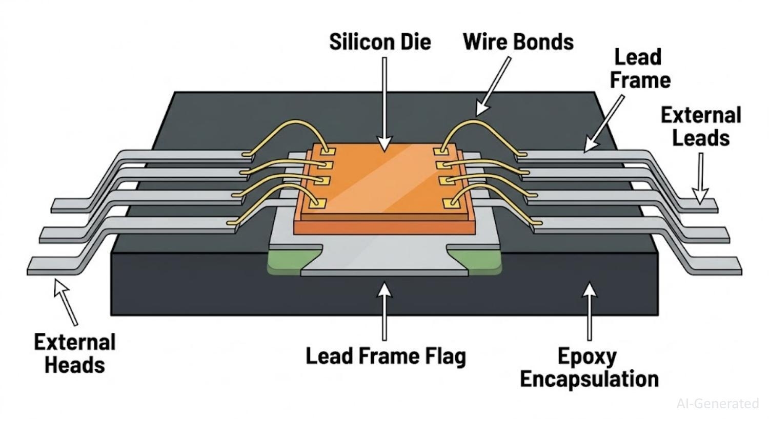
Figure: Internal structure of an IC package showing the silicon die, wire bonds, and external leads.
Why IC Packaging Matters
Selecting the wrong package early creates problems that are expensive to fix. Here is where the decision has the most real-world impact:
- Thermal performance: Packages like QFN and BGA have exposed thermal pads or die-attach areas that dramatically reduce junction-to-board thermal resistance. A QFN running a power regulator can dissipate heat 3–5× more efficiently than the same die in an SOIC.
- Signal integrity: In designs above 1 GHz, package lead inductance and interconnect length become parasitic elements. BGA packages with short, stubless interconnects outperform leaded packages at RF and high-speed digital frequencies.
- PCB footprint and assembly cost: A 100-pin LQFP occupies significantly more board area than a BGA with the same pin count - but BGAs demand finer trace routing and more rigorous assembly processes, raising per-board cost.
- Reliability: In harsh environments, through-hole DIP packages offer stronger mechanical attachment. In compact consumer electronics, CSP and WLP packages reduce board flex stress by minimising package mass.
Different Types of IC Packages: Quick Comparison
Note: Package outlines and naming conventions are standardized by JEDEC, ensuring uniformity and interoperability across electronic components.
| Package | Mount Type | Pin Count | Thermal | Cost | Rework | Typical Size | Typical Applications |
|---|---|---|---|---|---|---|---|
| DIP | Through-hole | 4–64 | Moderate | Low | Easy | 7.6–36 mm L | Prototyping, education, legacy industrial, socketed ICs |
| SOT-23 | SMD | 3–6 | Low–Mod | Low | Easy | 2.9×1.3 mm | Transistors, voltage refs, supervisors, single-gate logic |
| SOIC | SMD | 8–28 | Moderate | Low | Easy | 4–18 mm L | Op-amps, comparators, logic ICs, LDOs, gate drivers |
|
QFP/
LQFP |
SMD | 32–256 | Good | Medium | Medium | 7–28 mm sq. | Microcontrollers, DSPs, FPGAs (mid-range), ASICs |
| DFN | SMD | 2–16 | Excellent | Medium | Hard | 1–5 mm sq. | Power management, LDOs, current sense amps, sensors |
| QFN | SMD | 8–128 | Excellent | Medium | Hard | 2–12 mm sq. | RF SoCs, PMICs, wireless MCUs, motor drivers |
| LGA | SMD | 4–2000+ | Excellent | High | Medium | 3–45 mm sq. | Processors (CPU sockets), RF modules, MEMS sensors |
| BGA | SMD | 100–2000+ | Excellent | High | Very Hard | 5–45 mm sq. | CPUs, FPGAs, DDR memory, networking ASICs, SoCs |
| CSP | SMD | 16–400 | Good | High | Very Hard | ≤1.2× die area | Smartphones, wearables, IoT nodes, mobile PMICs |
| WLP | SMD | 4–200 | Good | High | Specialist | = die size | RF front-ends, MEMS, mobile power ICs |
| Flip Chip | SMD | 100–5000+ | Excellent | High | Specialist | Die-dependent | High-perf CPUs, GPUs, RF ICs, direct chip attach |
| SiP | SMD/Module | Variable | Depends | High | Specialist | 3–20 mm sq. | IoT modules, wearables, audio devices, smart sensors |
| 3D / TSV | SMD | 100–2000+ | Excellent | Very High | Specialist | Package-level | HBM memory, AI accelerators, chiplet processors |
How Many Types of IC Packages Are There?
There is no fixed number. IC packages fall broadly into three categories - through-hole, surface-mount, and advanced packaging - but within each, dozens of variants exist, and new sub-types continue to emerge as semiconductor nodes shrink.
JEDEC maintains the official package outline registry, which lists hundreds of standardised package families. In day-to-day PCB design, most engineers work with fewer than 15 types regularly. What keeps the count growing is the continuous push for higher pin density, lower profile, better thermals, and smaller footprint - often all at once.
The surface-mount category is where most of the action is in modern designs, so that is where the bulk of this guide focuses.
SMD IC Package Types: Quick Reference
Before the deep dives, here is a high-level overview of the five most common surface-mount IC packages:
- SOIC: Small Outline IC - the workhorse of logic and analog ICs. 1.27 mm pin pitch, gull-wing leads on two sides. Easy to hand-solder and inspect.
- QFP: Quad Flat Package - four-sided gull-wing leads for high pin counts. Standard for microcontrollers and DSPs. LQFP and TQFP are the most common variants.
- QFN: Quad Flat No-lead - thermally superior, compact footprint, no protruding leads. Widely used in wireless SoCs and power ICs. Requires reflow.
- BGA: Ball Grid Array - dominant for processors, FPGAs, and memory. Maximum pin density and signal integrity. Challenging rework and inspection.
- CSP: Chip Scale Package - package area within 1.2× of the die. Used in wearables, mobile devices, and compact IoT hardware.
Surface Mount IC Package Types
Surface-mount IC package types dominate modern PCB design. These SMD IC package types support automated pick-and-place, enable fine-pitch components, and generally deliver better electrical performance than through-hole alternatives.
Small Outline Packages: SOIC, SOP, SSOP, TSSOP, SOT
SOIC / SSOP / TSSOP:
The SOIC family is one of the most common SMD IC package types across analog and digital design. Standard SOIC runs at 1.27 mm pin pitch with gull-wing leads on two sides.
SSOP (Shrink Small Outline Package) tightens the pitch to 0.65 mm.
TSSOP (Thin Shrink Small Outline Package) reduces body height further for low-profile applications.
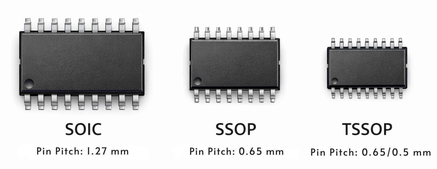
Figure: Comparison of SOIC, SSOP, and TSSOP SMD IC package sizes and pin pitches.
Note
Why they're still popular: These packages remain popular because they are visually inspectable after soldering and manageable with hand soldering tools. They suit op-amps, comparators, voltage regulators, gate drivers, and logic ICs well. The constraint is pin count - typically 8 to 28 - and a larger footprint than QFN for the same function. Understanding how SMD component markings relate to package dimensions is essential when reading datasheets. For example, resistor package sizes and codes follow standardized markings (see SMD resistor code guide).
SOT-23 / SOT-89 / SOT-223:
SOT (Small Outline Transistor) packages belong to this same family despite the transistor-centric name - they are widely used for low-pin-count ICs, voltage references, single-gate logic, and small signal MOSFETs.
SOT-23 is the most common variant, with three pins on a 0.95 mm pitch in a 2.9 × 1.3 mm body. SOT-23-5 and SOT-23-6 extend this to five or six pins for small op-amps and supervisory ICs.
SOT-89 and SOT-223 are larger power variants with a heat-dissipation tab for higher current applications.
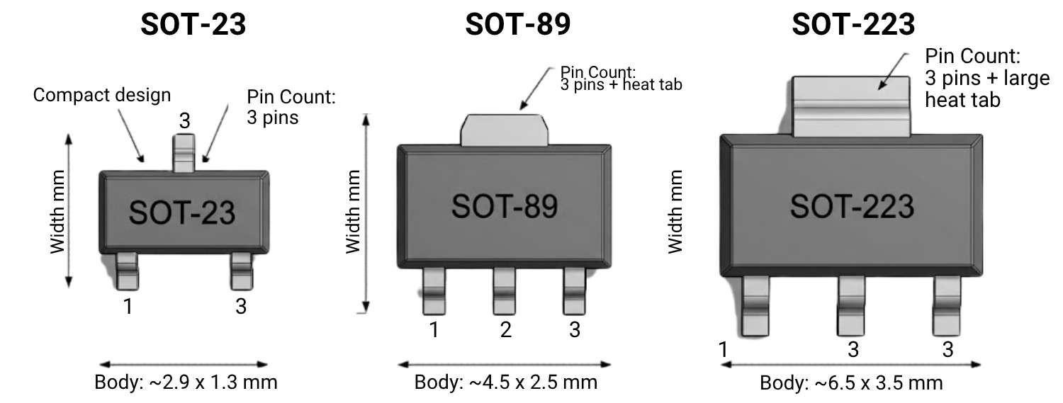
Figure: SOT-23, SOT-89, SOT-223 pin comparison
Note
Assembly note: SOT packages are among the most hand-solderable SMD packages available. The large pad-to-pad spacing relative to the package size makes them accessible even for engineers transitioning from through-hole work. They appear on almost every modern PCB in some form - as bypass capacitor discharge paths, reset supervisors, or discrete level-shifting transistors.
Quad Flat Packages: QFP, LQFP, TQFP
QFP / LQFP / TQFP:
Quad Flat Packages extend the SOIC concept to all four sides, enabling much higher pin counts.
LQFP is the dominant variant in embedded design - the STM32 family alone ships in LQFP-48, LQFP-64, LQFP-100, and LQFP-144 configurations. Pitch ranges from 0.4 mm to 0.8 mm depending on the variant.
TQFP (Thin Quad Flat Package) is a thinner, low-profile version of QFP, used in space-constrained designs where height is limited. Pitch ranges from 0.4 mm to 0.8 mm depending on the variant.
Handling and assembly: QFP packages offer a solid balance of capability and accessibility: joints are visually inspectable, rework is feasible with hot-air stations, and the packages are compatible with standard FR4 processes. The main fragility point is the exposed leads - they bend during rough handling, so careful ESD and mechanical protection during assembly is essential.
High-frequency limit: In high-frequency designs above a few hundred MHz, QFP lead inductance starts limiting performance. That is typically the trigger to move toward BGA.
Quad Flat No-lead (QFN)
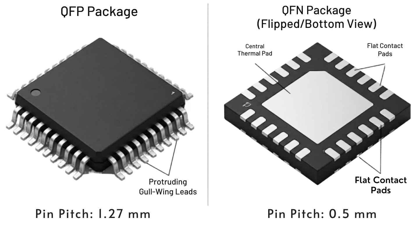
Figure: Comparison between QFP and QFN surface mount IC packages.
QFN has displaced SOIC in many applications where thermal performance or compact size is a priority. There are no protruding leads - contact pads sit flush on the package underside, and a large exposed thermal pad in the centre connects directly to the die attach area.
Thermal performance: The exposed thermal pad is QFN's greatest strength and its primary assembly challenge. When properly reflowed onto a PCB with a matched thermal via array, QFN can achieve junction-to-board thermal resistance (θJB) as low as 3–5°C/W on a 4-layer board. This makes it ideal for power management ICs, RF transceivers, and motor driver chips.
Solder voiding (key assembly risk): The challenge is solder voiding under the thermal pad. IPC-7093 recommends limiting voiding to below 25% of the pad area to maintain thermal performance. Proper stencil aperture design - typically 50–70% of the pad area, split into multiple smaller openings - is critical for achieving this reliably in SMT assembly. Reading up on solder pad design is highly recommended for understanding the geometries that minimise voids in QFN layouts.
Dual Flat No-lead (DFN)
DFN (Dual Flat No-lead) is essentially QFN with contacts on only two opposing sides instead of all four. The result is a smaller package outline that suits low-to-medium pin count ICs where a full quad perimeter would be wasteful. Common DFN configurations run from 2-pin (DFN-2, used in temperature sensors and single diodes) up to 14 or 16 pins for multi-channel analog ICs and small microcontrollers.
Assembly and use cases: Like QFN, DFN packages often include a central exposed thermal pad. The assembly rules are identical - the package requires reflow soldering, the thermal pad needs a via array connecting to the ground plane, and inspection relies on the same X-ray or cross-section methods. DFN is widely used in power management ICs, current-sense amplifiers, and low-noise LDOs, where a compact footprint and good thermal dissipation matter, but the pin count does not justify a full QFN outline.
Ball Grid Array (BGA IC Package)
The BGA IC package replaces perimeter leads with an array of solder balls on the underside, enabling far higher pin counts in a smaller footprint. A 17×17 mm BGA can carry 400 or more connections - something impossible with QFP at standard pitches.
Where BGA excels: BGAs dominate wherever high pin count and high-speed signalling coincide: processors, FPGAs, DDR memory, networking ASICs, and complex SoCs. The short interconnect from die pad to solder ball reduces package inductance directly, which benefits signal integrity at gigahertz frequencies.
Assembly challenge: The trade-off is assembly and inspection complexity. BGA joints sit under the package and cannot be visually verified after reflow - X-ray inspection (2D or 3D CT) is the standard method. Rework requires specialised BGA stations with controlled thermal profiles and reballing capability. For a deeper dive into variants including PBGA, CBGA, and flip-chip configurations, reviewing a detailed BGA package types guide is a solid technical step.
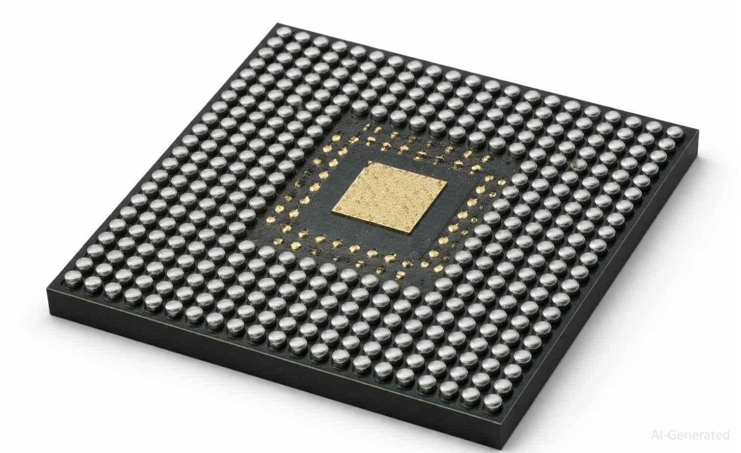
Figure: Underside of a BGA IC package showing the array of solder balls used for surface mount assembly.
Land Grid Array (LGA)
LGA is structurally similar to BGA but replaces the pre-formed solder balls with flat land pads on the package underside. The solder is deposited on the PCB pads or applied via a solder paste stencil - the package itself carries no solder. Intel’s desktop processor sockets (LGA1700, LGA1851) are the most recognised examples of LGA in large format, but the package type also appears in compact form for wireless modules, RF transceivers, and MEMS sensors.
LGA vs BGA trade-offs: The advantage over BGA is that LGA avoids ball collapse variability during reflow and allows a lower stand-off height, which can improve thermal coupling to a heatsink. The disadvantage is that joint coplanarity depends entirely on the PCB pad and stencil quality, rather than pre-formed solder balls providing a self-levelling effect. LGA rework is generally easier than BGA since the package lands can be cleaned and re-pasted without a reballing step.
Chip Scale Package (CSP)
CSP represents the end of SMD miniaturization and is covered in detail in the advanced packaging section below.
Through-Hole IC Package Types
Through-hole packages fell out of favour for high-density production in the 1990s, but they remain relevant for prototyping, high-reliability hardware, and environments where mechanical robustness matters more than footprint.
Dual In-line Package (DIP)
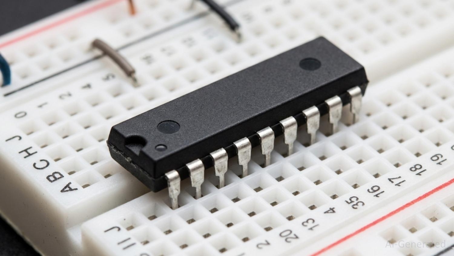
Figure: A 16-pin DIP IC package inserted into a prototyping breadboard.
DIP is the most recognisable IC package in electronics education. Two parallel rows of pins at 2.54 mm (100 mil) pitch plug directly into breadboards or DIP sockets, making it the fastest way to validate circuit behaviour without soldering.
In production, DIP use has narrowed considerably. You still find them in through-hole optocouplers, some op-amps, relay drivers, and legacy industrial hardware that has not been redesigned. For new designs, DIP is chosen specifically when breadboard compatibility or socketed field replacement is an explicit requirement. Pin counts range from 4 to 64; the 8-pin, 14-pin, and 16-pin variants are most common.
SIP and ZIP Packages
Single In-line Packages (SIP) carry one row of pins and are used for memory modules, resistor networks, and some hybrid power modules. Zigzag In-line Packages (ZIP) angle alternate pins to allow higher pin density while maintaining through-hole mounting.
Both see limited use in modern designs. The main advantage is a very narrow PCB footprint when board height is not constrained - useful in edge-mounted or vertical component configurations.
Advanced IC Packaging Types: Next-Generation Technologies
As transistor scaling faces physical limits, packaging innovation has become a primary driver of system performance. These technologies define the current frontier.
Chip Scale Package (CSP)
A CSP is defined as any package whose footprint area is no more than 1.2 times the area of the die. This near-zero packaging overhead makes CSP the dominant choice for space-constrained applications: smartphones, wireless earbuds, and compact wearables.
CSPs use a land grid array or fine-pitch ball array. Mounting requires 0.4 mm or finer ball pitch, which demands tight PCB fabrication tolerances and a controlled reflow profile to avoid bridging or open joints. Underfill is frequently recommended for CSP in applications with high mechanical shock or thermal cycling, as the small stand-off height concentrates fatigue stress at the solder joints.
Wafer-Level Packaging (WLP)
WLP takes CSP to its logical limit: the entire packaging process, including redistribution layers and solder-bump formation, is performed at the wafer level before die singulation. The resulting package is literally the same size as the die.
WLP is standard in RF front-end modules, MEMS sensors, and power management ICs in mobile devices. Very short interconnects reduce parasitic inductance, improving high-frequency performance. The downside: die size limits cap pin count, and WLP dies are mechanically fragile without underfill protection after board mounting.
System-in-Package (SiP)
SiP integrates multiple dies - processor, memory, RF module, PMIC, passives - into a single package. Unlike a System-on-Chip (SoC), where all functions share a single die, SiP allows heterogeneous integration: different process nodes and die types are assembled.
Apple's AirPods, Nordic Semiconductor's nRF modules, and many IoT edge devices use SiP to achieve complete sub-system functionality in a package smaller than a fingernail. For a PCB designer, a SiP simplifies the board layout dramatically - but it locks in whatever the vendor has integrated.
Flip Chip
Flip chip is an interconnect method rather than a standalone package family, but it underpins a large proportion of advanced IC packages including flip-chip BGA (fcBGA), flip-chip CSP (fcCSP), and direct chip attach (DCA).
The core idea is straightforward: instead of bonding the die face-up and connecting it to the package substrate with wire bonds, the die is flipped face-down. Solder bumps or copper pillars on the active face of the die connect directly to the substrate pads.
The electrical advantage is significant. Wire bond interconnects introduce inductance in the range of 1-3 nH per bond wire, which limits performance above a few gigahertz. Flip chip copper pillar bumps reduce interconnect inductance to the picohenry range, which is why virtually every high-performance processor, GPU, and FPGA manufactured today uses flip chip attach. The thermal path also improves because the die backside faces upward, making direct contact with a heatsink or thermal interface material straightforward.
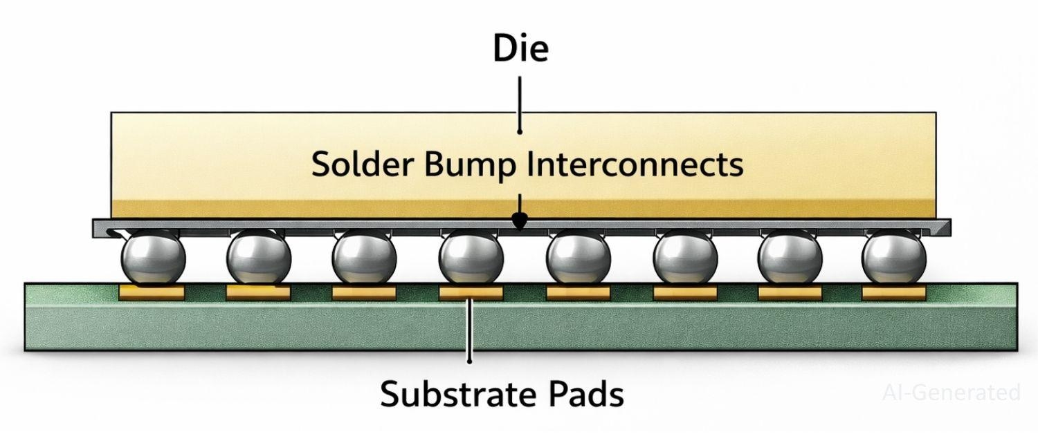
Figure: A flip chip IC package showing die face-down with solder bump interconnects.
From a PCB designer’s perspective, a flip chip device typically arrives as an fcBGA or fcCSP - the flip chip attach is internal to the package. The external footprint and assembly rules follow BGA or CSP conventions. Where flip chip becomes a direct PCB concern is in direct chip attach applications for high-volume consumer electronics, where bare dies are mounted directly onto the PCB substrate using underfill to manage the CTE mismatch between silicon and FR4.
3D Packaging and Die Stacking
3D packaging stacks multiple dies vertically within a single package, interconnecting them through the silicon itself rather than routing signals out to a package substrate and back in. The key enabling technology is Through-Silicon Vias (TSVs) - vertical copper-filled channels etched through the die that carry signals between stacked layers at extremely short distances.
High Bandwidth Memory (HBM) is the most commercially prominent application. HBM stacks four or more DRAM dies vertically using TSVs and connects them to a logic die (GPU, AI accelerator, or network ASIC) through a silicon interposer on the same package substrate.
The result is memory bandwidth that exceeds 1 TB/s - a figure impossible to achieve with conventional GDDR or LPDDR packages operating over PCB traces. AMD’s Instinct accelerators, NVIDIA’s H100, and Intel’s Ponte Vecchio all use HBM in 3D stacked configurations.
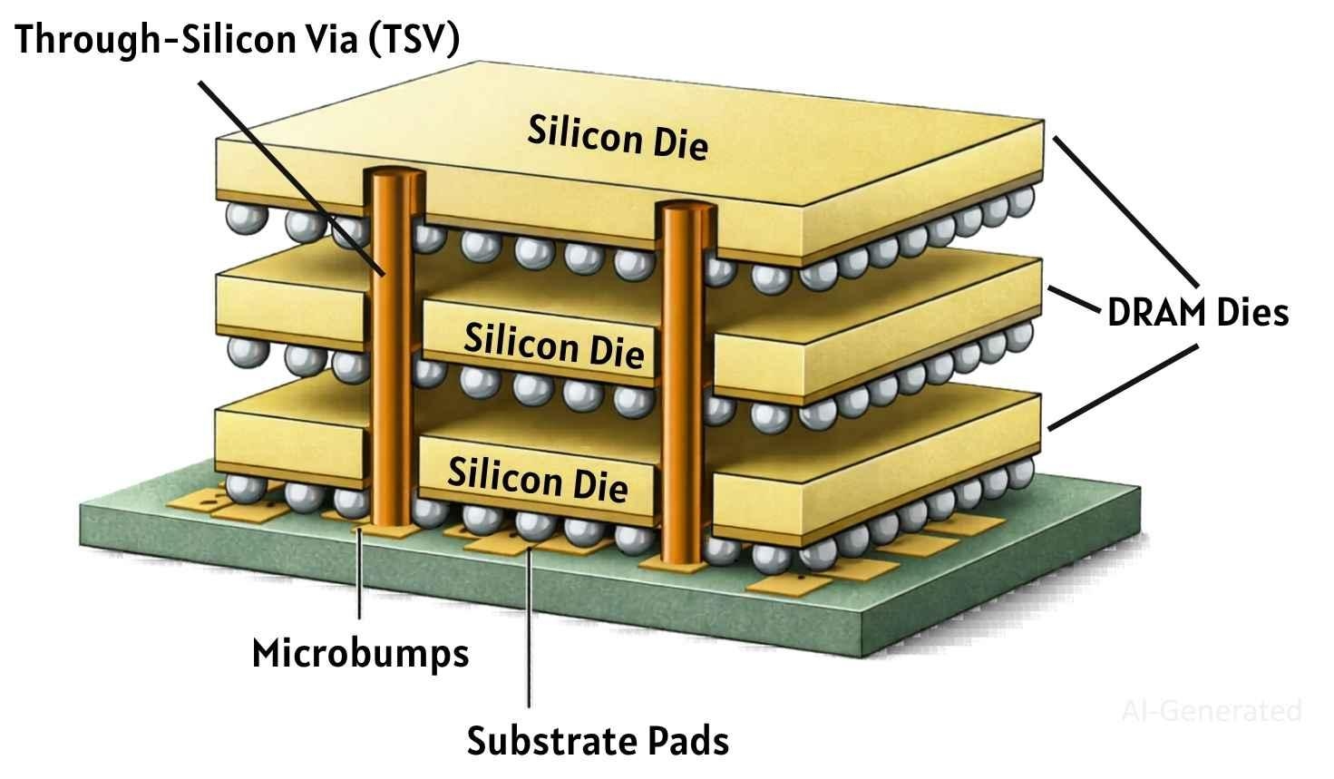
Figure: 3D packaging diagram showing vertically stacked silicon dies connected via Through-Silicon Vias (TSVs).
A related concept is the chiplet architecture, where a processor is disaggregated into multiple smaller dies (chiplets) connected through an advanced packaging interconnect rather than integrated on a single monolithic die. AMD’s 3D V-Cache technology stacks additional SRAM cache directly on top of a CPU compute die using TSVs. Intel’s EMIB (Embedded Multi-die Interconnect Bridge) embeds a silicon bridge inside the package substrate to connect chiplets at near-monolithic bandwidth without requiring a full silicon interposer.
For most PCB designers, 3D stacked packages and chiplet devices arrive as standard BGA or LGA footprints - the stacking is internal to the package. The PCB-level considerations are the same as any high-density BGA: controlled impedance routing, power delivery network design, and X-ray inspection for assembly verification.
Where 3D packaging directly affects board design is in the power delivery requirements: stacked dies with high transistor counts in a small footprint generate significant localised heat flux, demanding careful thermal via placement and heatsink mounting design.
IC Packaging in Real Projects (Practical Examples)
ESP32 → QFN
Espressif's ESP32 ships in a 5×5 mm QFN-48 package. The reasoning is practical: the chip needs RF performance (short interconnects help at 2.4 GHz), efficient thermal dissipation during active Wi-Fi transmission, and a compact footprint for IoT nodes. The exposed thermal pad connects to a GND copper pour with thermal vias, keeping junction temperature in check during burst transmissions.
If you are working on a custom board, reading up on how to design an ESP32-S2 module PCB covers the specific layout considerations for thermal pad via stitching and RF trace routing.
STM32 → LQFP or BGA
STMicroelectronics offers the STM32H7 core in both LQFP-144 and TFBGA-240. The LQFP variant fits prototyping and low-to-medium volume designs - hand-reworkable, visually inspectable, compatible with two-layer PCBs in some configurations. The BGA variant targets high-density industrial and communication hardware where pin count exceeds what LQFP can provide, or board area is tightly constrained.
DDR Memory → BGA
LPDDR4X and DDR5 memory chips exist exclusively in BGA packages. Pin counts often exceed 200, and signal speeds (3200 MT/s and above) make BGA the only viable option. Trace length matching, reference plane continuity, and via stub management become non-negotiable PCB requirements when working with these devices.
How to Choose the Right IC Package for Your PCB
Several factors should drive the selection:
- Assembly method: If you are hand-soldering prototypes, DIP and SOIC are realistic choices. QFP is manageable with a fine-tipped iron and flux. QFN and BGA require reflow - attempting BGA assembly without X-ray verification creates reliability risks that are very difficult to debug later.
- Thermal requirements: Calculate the required θJA based on power dissipation and maximum ambient temperature. If you need θJA below 30°C/W at significant power levels, QFN or BGA with thermal vias is likely necessary. SOIC and QFP packages generally will not satisfy tight thermal budgets.
- Signal speed: For designs operating above 500 MHz or with rise times below 1 ns, package parasitic inductance matters. BGA and QFN are the right choices. QFP at 0.4 mm pitch is usable to a few GHz; beyond that, BGA is standard.
- Manufacturing cost and volume: BGA assembly, X-ray inspection, and rework all add per-board cost. At prototype or low-volume stages, LQFP or QFN is often more economical even when BGA is the eventual production target. The comprehensive PCB assembly service at JLCPCB supports both low-volume runs and higher-volume production without requiring a supplier change between stages.
- Component availability: Some microcontrollers and power ICs are available in DIP, SOIC, and QFN simultaneously. Others - especially high-end SoCs and memory - exist in BGA only. Component availability should always be verified early. Platforms like JLCPCB Parts allow you to filter components by package type (QFN, BGA, LQFP), ensuring your selected IC is both available and compatible with your assembly process.
Common Mistakes Engineers Make When Selecting IC Packages
Ignoring Thermal Pad Design on QFN
The thermal pad is not optional and is not just a mechanical anchor. Leaving it unconnected or using a solid copper pad without thermal vias defeats the purpose of choosing QFN in the first place. The pad needs a via array connecting to internal ground planes, and the stencil aperture must be designed to control solder volume and minimise voiding below the IPC-7093 threshold of 25%.
Choosing BGA Without Proper Assembly Infrastructure
BGA is straightforward on a professional SMT line with controlled reflow, ENIG surface finish, and X-ray inspection. Without those, it is a liability. Teams that adopt BGA for a prototype without inspection capability frequently end up with intermittent connection failures that are extremely difficult to root cause. Checking standard reflow soldering processes covers the profile parameters most critical for BGA joint quality.
Overcomplicating Prototypes
Using BGA in an early prototype when the same IC is available in QFP slows down iteration unnecessarily. The practical principle: use the most accessible package during development, then migrate to the optimised production package after design validation. Skipping this step in the name of "designing for production from day one" regularly results in debugging sessions that would have been trivial with a leaded package.
Mismatching PCB Capability to Package Requirements
Fine-pitch QFP (0.4 mm) and micro-BGA (0.4 mm ball pitch) require PCB trace and space widths down to 75–100 μm. Not all fabricators can reliably hold these tolerances. Confirm minimum feature sizes with your manufacturer before committing to a package that demands them. Using a tool like JLCPCB's quotation page lets you verify manufacturability against your specific stackup before finalising package selection.
From IC Package Selection to PCB Assembly: How JLCPCB Supports Your Project
Understanding IC package types is the design side of the equation. Getting them assembled correctly and cost-effectively is where the manufacturing partner matters. Combined with its parts sourcing platform, JLCPCB enables a seamless transition from package selection to fully assembled PCB.
One-Stop PCB Manufacturing and Assembly
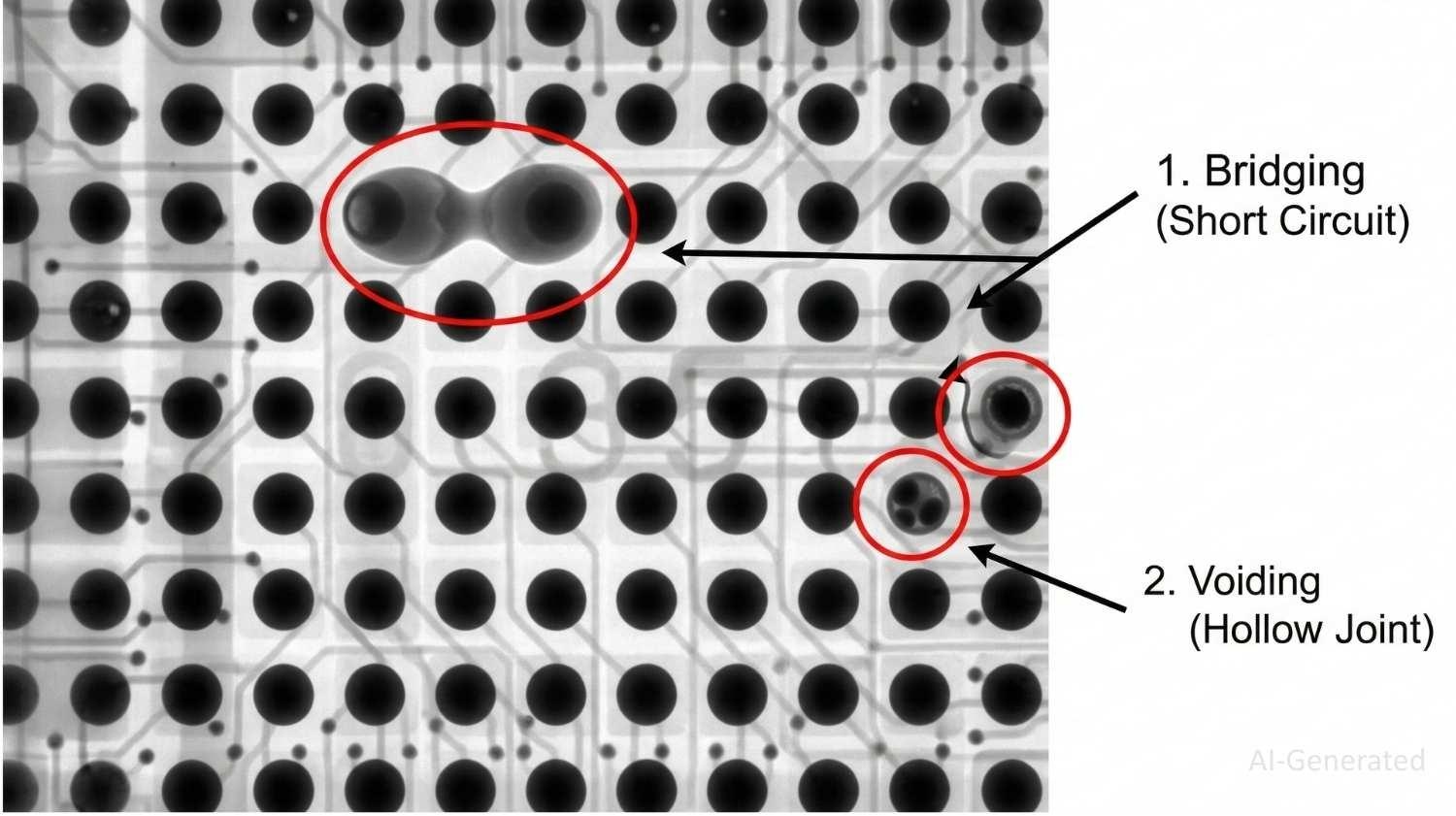
Figure: X-ray inspection image verifying solder joint integrity under a BGA IC package.
For packages like QFN and BGA, assembly quality directly impacts reliability. JLCPCB integrates X-ray inspection and controlled reflow profiling to ensure solder joint integrity across the full range of packages covered in this guide - QFN, BGA, QFP, SOIC, and CSP on the surface-mount side, plus through-hole DIP and SIP components for mixed-technology boards. For BGA specifically, automated optical inspection (AOI) and X-ray verification are part of the standard assembly process, which is critical for confirming joint quality without destructive testing.
Component Sourcing Integration
The JLCPCB Parts Library includes components pre-matched to assembly capabilities. When your BOM calls for a QFN-packaged MCU or a BGA memory device, the database reflects actual stock availability and footprint compatibility - reducing the risk of package mismatch errors appearing mid-order.
DFM and Engineering Support
Design-for-manufacturing checks at JLCPCB flag common package-related issues before fabrication starts: insufficient solder mask clearance around BGA pads, missing thermal via arrays under QFN thermal pads, or QFP pad geometries too narrow for reliable paste deposition. Catching these at the DFM stage avoids the costly cycle of assemble → fail → redesign → reassemble.
If you are expanding your production capabilities, understanding the best practices for scaling your PCBA prototype to low-volume production outlines the process checkpoints that matter as complexity and volume increase.
FAQs
Q: What are the different types of IC packages?
IC package types fall into three main categories: through-hole (DIP, SIP), surface-mount (SOIC, QFP, QFN, BGA), and advanced packaging (CSP, WLP, SiP). Within each category, multiple variants exist based on pin count, pitch, thermal design, and form factor.
Q: What is the most commonly used IC package?
In modern electronics production, QFN and BGA dominate high-volume consumer electronics and computing hardware. For general-purpose digital and analog ICs, SOIC and LQFP remain extremely common. The most-used package depends heavily on the application segment.
Q: What is a BGA IC package used for?
BGA is used where high pin count, high-speed signal integrity, and thermal performance are all required simultaneously. Typical applications include processors, FPGAs, DDR memory, networking ASICs, and complex SoCs. It is not suitable for designs that lack X-ray inspection capability or proper reflow infrastructure.
Q: Which IC package is best for beginners?
DIP is the most accessible - breadboard-compatible, hand-solderable, and physically robust. SOIC is the recommended step up when moving to SMD, since its 1.27 mm pitch tolerates hand soldering with a fine tip and flux. QFN and BGA should be attempted only after gaining experience with leaded SMD packages.
Q: What is the difference between QFN and QFP?
QFP has gull-wing leads extending from all four sides of the package body, making it visually inspectable and hand-reworkable. QFN has no protruding leads - pads sit flush on the package underside, along with a central thermal pad. QFN delivers better thermal performance and a smaller footprint than equivalent-pin-count QFP, but requires reflow soldering and cannot have its thermal pad verified visually without X-ray equipment.
Conclusion
IC package selection is a design decision with long-term consequences. The package you choose defines your thermal management strategy, sets the floor on your assembly process complexity, and determines whether rework is feasible in the field.
Getting it right from the start requires understanding what each package family actually optimises for - not just what it looks like in a datasheet diagram. In practice, package selection is a trade-off between thermal performance, manufacturability, and cost - not just footprint.
For most new designs: SOIC or QFP for straightforward digital and analog functions, QFN when thermal performance in a compact footprint is needed, and BGA when pin count or signal speed demands it. Avoid BGA in prototypes unless you have access to proper assembly and inspection infrastructure.
When you are ready to move from schematic to assembled boards, check out JLCPCB to see assembly pricing for your specific package mix. The platform supports every package type discussed in this guide - from through-hole DIP to fine-pitch BGA - with DFM checks built into the order workflow.
- Supports every package type discussed in this guide - from through-hole DIP to fine-pitch BGA
- With DFM checks built into the order workflow.
Popular Articles
• Common PCB Assembly Methods and Soldering Techniques Explained
• What Is BGA Void? Causes, IPC Limits, and Solutions
• SMD Soldering Tools You Need: Complete Guide from Beginner to Pro
• Reflow Soldering: Everything You Need to Know
• SMT Assembly Process Explained and Equipment Used: A Step-by-Step Guide to PCBA Manufacturing
Keep Learning
12 Professional Soldering Tips and Tricks Every Beginner Should Know
Soldering is not merely "gluing" metal; it is a metallurgical process that creates an intermetallic compound (IMC). This molecular bond ensures the electrical and mechanical integrity of your device. A poor joint might pass a quick visual check but will inevitably fail under vibration or thermal stress, leading to "ghost" bugs and hardware failures. These soldering tips and tricks focus on practical, repeatable techniques used in professional electronics soldering—from correct heat transfer and flux u......
Solder Melting Point Guide: Chart, Alloy Types, and Reflow Considerations
In the precise world of electronics manufacturing, a difference of just a few degrees can mean the distinction between a perfect, reliable solder joint and a catastrophic "cold" joint failure. While many hobbyists view soldering simply as "melting metal to stick things together," professional PCB assembly requires a nuanced understanding of thermodynamics. The solder melting point is not simply a single value listed in a datasheet; it is a decisive limit that determines the choice of components, the s......
The Ultimate Guide to Solder Flux: Everything You Should Know Before Soldering PCB
Soldering is needed to make almost all electronic devices. Adding solder alone won't make a joint that is strong, clean, and sound from a metallurgical point of view. Solder flux is a very important part of the process that comes in here. If you want to do your job better and make it more reliable, you need to know a lot about soldering flux, whether you're an engineer, a professional technician, or just a hobbyist. This article goes into a lot of detail about solder flux, including what it is, how it......
Common PCB Assembly Methods and Soldering Techniques Explained
Whether you're designing your first prototype or scaling up to production, understanding PCB assembly methods and soldering techniques is crucial to achieving reliable, high-performance circuit boards. Modern PCBA primarily relies on Surface Mount Technology (SMT) and Through-Hole Technology (THT)—each offering unique advantages for component density, durability, and manufacturability. In this guide, we'll break down the major PCB assembly methods, key soldering techniques such as reflow and wave sold......
Flex PCB Assembly Guide: Process, Challenges, and Solutions
Flexible Printed Circuit Boards (Flex PCBs) are the foundational technology enabling the compact, innovative design of modern electronics. Because of their ability to bend and fold, they power devices from smart wearables to compact medical instruments where traditional rigid printed circuit boards (Rigid PCBs) can't be used. Achieving a functional electronic circuit from the raw plastic film demands special expertise, with flexible PCB assembly (FPCA) representing the crucial final step in this trans......
SMD Rework Guide: Tools, Temperatures, and Techniques That Prevent PCB Damage
From replacing a burned regulator to correcting wrong component values or removing solder bridges on fine-pitch ICs, SMD rework is an essential skill in electronics manufacturing and prototyping. It allows engineers to repair assembly defects, implement design changes, and recover valuable PCBs without the cost and delay of building new boards. In this guide, you will learn: What SMD rework is Common rework scenarios Tools and temperatures Safe removal and installation Package-specific techniques Real......