
Wire Bonding vs Flip Chip: Key Differences in Semiconductor Packaging
17 min
- Wire Bonding vs Flip Chip: Key Differences
- Wire Bonding vs Flip Chip: Cost Comparison
- What Is Wire Bonding?
- What Is Flip Chip Packaging?
- Advantages of Wire Bonding
- Advantages of Flip Chip Technology
- Wire Bonding Limitations
- Flip Chip Manufacturing Challenges
- Applications of Wire Bonding and Flip Chip
- Future Trends in Semiconductor Packaging
- FAQ About Wire Bonding and Flip Chip
- Conclusion
In the rapidly evolving world of semiconductor packaging, the choice between Wire Bonding and Flip Chip technology is more than just a mechanical decision—it is a strategic pivot that dictates your product’s performance, thermal limits, and bottom line.
Are you looking for the cost-effective reliability of traditional interconnects, or does your application demand the high I/O density and superior signal integrity of modern flip-chip architectures?
In this comprehensive guide, we draw on years of high-level packaging engineering experience to strip away the complexity. We will dive deep into the structural mechanics, cost trade-offs, and electrical characteristics of wire bonding and flip chip.
By the end of this article, you will have a clear, engineering-backed roadmap to determine whether wire bonding or flip chip aligns with your specific design requirements and market goals.
Wire Bonding vs Flip Chip: Key Differences
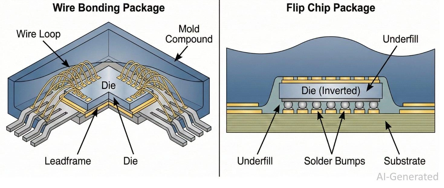
While Wire Bonding relies on peripheral connections using fine metal wires (Gold, Copper, or Aluminum), Flip Chip technology involves "flipping" the die face-down to connect directly to the substrate via conductive "bumps" distributed across the entire surface of the chip.
The following table provides a high-level technical comparison to help you distinguish between these two pillars of semiconductor packaging:
Feature | Wire Bonding | Flip Chip |
|---|---|---|
Interconnect Method | Loops of fine wire (Au, Cu, Al) | Solder bumps or copper pillars |
Connection Type | Peripheral (usually around the edges) | Area Array (entire die surface) |
I/O Density | Limited (lower pin count) | High (maximum I/O per unit area) |
Signal Integrity | Higher inductance (due to wire length) | Low inductance (short path) |
Thermal Performance | Moderate (relies on substrate) | Excellent (direct thermal path) |
Footprint Size | Larger (requires space for loops) | Minimal (package-scale or near-die size) |
Process Maturity | Very High (Standard for decades) | High (Standard for HPC & Mobile) |
Repairability | Possible (wires can be replaced) | Difficult to Impossible (underfilled) |
Key Takeaway for Engineers
If your design targets cost-sensitive applications with moderate pin counts (such as basic microcontrollers or power discretes), Wire Bonding remains the gold standard.
However, for high-frequency or high-power applications (like CPUs, GPUs, or 5G RFICs), the parasitic inductance of a bond wire becomes a bottleneck, making Flip Chip the necessary choice.
Wire Bonding vs Flip Chip: Cost Comparison
In semiconductor packaging, cost is a function of volume, complexity, and the specific performance requirements of the silicon.
Manufacturing Cost Factors
The cost delta between these two technologies is primarily driven by the interconnect density and substrate requirements:
- Substrate Complexity: Wire bonding typically uses simpler, lower-layer-count organic substrates or leadframes. Flip chip requires high-density interconnect (HDI) substrates with fine line/space capabilities to match the bump pitch on the die, which significantly drives up the BOM (Bill of Materials).
- Consumables: Wire bonding uses precious metals (Gold, Silver-plated Copper). While the amount per chip is small, at scale, fluctuating gold prices can impact margins. Flip chip uses solder bumps or copper pillars, which are cheaper as materials but require expensive wafer-level processing (WLP).
Equipment and Process Complexity
- Wire Bonding: This is a sequential process. Each wire is bonded one by one. While modern bonders are incredibly fast (up to 20+ wires per second), the process time increases linearly with the number of I/Os.
- Flip Chip: This is a "mass reflow" process. Whether the chip has 100 or 10,000 bumps, they are all connected simultaneously during the reflow cycle. However, the upfront investment in wafer bumping lines and high-precision flip-chip bonders is substantially higher than a standard wire bonding floor.
Cost Considerations for Different Applications
Application Tier | Preferred Technology | Cost Logic |
|---|---|---|
Low-End/Discrete | Wire Bonding | Low I/O count makes leadframe-based wire bonding unbeatable in price. |
Mid-Range IoT/MCU | Wire Bonding | Mature infrastructure and high yield rates keep total cost of ownership (TCO) low. |
High-Performance (SoC/GPU) | Flip Chip | Although the unit cost is higher, the performance gains (speed/thermal) justify the premium. |
Engineer's Tip: When calculating cost, don't forget the "Silicon Real Estate" factor. Flip chip allows for a smaller die size because you don't need a large "bond pad" ring around the perimeter. Sometimes, the savings in silicon area can offset the higher packaging cost.
What Is Wire Bonding?
Wire bonding is the industry’s most established method of creating electrical interconnections between a semiconductor die and its packaging substrate or leadframe.
Wire bonding is a solid-state welding process that uses a combination of heat, pressure, and ultrasonic energy to create a bond between a thin wire and a metalized pad on the chip (the die) and the corresponding lead on the package.
Because it is a "looping" technology, the wires arch through the air before landing on their target, which is a defining characteristic of this method.
How Wire Bonding Works in Semiconductor Packaging
The process generally follows a sequence of high-speed mechanical movements. There are two primary types of bonding:
Common Materials Used in Wire Bonding
The choice of wire material directly impacts both cost and electrical performance:
- Gold (Au): The traditional standard. It is highly conductive, resists corrosion, and is soft enough to bond easily. However, its high cost makes it less attractive for high-volume consumer goods.
- Copper (Cu): The modern high-volume favorite. It offers superior electrical conductivity and thermal stability compared to gold at a fraction of the cost. The trade-off? It is harder and requires an inert gas (like Nitrogen) during bonding to prevent oxidation.
- Aluminum (Al): Typically used in "Large Wire" bonding for power modules (like those in EV inverters) because of its ability to handle high currents and its compatibility with ceramic substrates.
- Silver (Ag): An emerging middle-ground material that offers better conductivity than gold but at a lower price point than pure Au.
Engineering Note on Substrate Prep:
Successful wire bonding, especially for Chip-on-Board (COB) designs, heavily relies on the quality of the PCB surface finish. To ensure high bond pull strength and prevent oxidation, using a high-quality finish like ENIG (Electroless Nickel Immersion Gold) or ENEPIG is critical.
JLCPCB provides industry-leading ENIG surface finishes with precise thickness control, ensuring that your wire-bonded prototypes maintain maximum conductivity and long-term reliability.
Learn more about JLCPCB’s PCB Manufacturing & Assembly Capabilities
What Is Flip Chip Packaging?
If wire bonding is the "wiring" of a house, Flip Chip is the "plug-and-socket" approach. By eliminating the long, looping wires of traditional packaging, Flip Chip allows for a more compact, higher-performance connection.
Flip Chip, also known as Controlled Collapse Chip Connection (C4), is a method for interconnecting semiconductor devices, such as IC chips and microelectromechanical systems (MEMS), to external circuitry with solder bumps that have been deposited onto the chip pads.
The "Flip" in the name comes from the process of inverting the chip so that its top side faces down toward the substrate, allowing the bond pads on the chip to align directly with the pads on the PCB or substrate.
How Flip Chip Interconnection Works
The process is fundamentally different from the point-to-point "sewing" motion of wire bonding:
Flip Chip Structure and Components
- The Die (Silicon): The active semiconductor device.
- Under Bump Metallization (UBM): A thin metal layer between the chip pad and the solder bump that ensures good adhesion and acts as a diffusion barrier.
- Conductive Bumps: The actual "bridge" for the signal. Modern high-end chips often use Copper Pillars with solder caps for even finer pitch and better thermal performance.
- Underfill: The "glue" that protects the bumps from cracking due to Coefficient of Thermal Expansion (CTE) mismatches between the silicon and the organic substrate.
Advantages of Wire Bonding
Lower Manufacturing Cost
For most low-to-medium I/O applications, wire bonding is significantly cheaper than flip chip.
- No Wafer Bumping Required: You don't need the expensive "bumping" step at the wafer level.
- Inexpensive Substrates: Wire bonding works perfectly with simple leadframes or low-layer-count PCBs, which are far cheaper than the high-density substrates required for flip chip.
- Material Flexibility: Engineers can switch between Gold, Copper, or Silver wires depending on the budget and performance needs.
Mature and Reliable Process
Wire bonding has been the industry standard for over 50 years.
- High Yield Rates: The process is extremely stable, with modern equipment achieving near-perfect yields.
- Established Infrastructure: Almost every OSAT (Outsourced Semiconductor Assembly and Test) facility in the world has rows of wire bonders ready to go. There is no "learning curve" for this technology.
- Inspection Ease: Unlike flip chip, where the connections are hidden under the die, wire bonds are visible. They can be inspected optically or via X-ray with high confidence.
Suitable for Many Semiconductor Devices
Wire bonding isn't just for "old" tech; it is incredibly flexible for specific modern designs:
- Stacked Die (SiP): Wire bonding is excellent for stacking multiple chips in a single package (System-in-Package). You can easily "staircase" wires from different levels.
- Variable Heights: If you have components of different heights on a substrate, wires can easily bridge the gap.
- Power Electronics: Using heavy Aluminum ribbons or thick wires allows for high current carrying capacity, which is essential for EV power modules and industrial inverters.
Advantages of Flip Chip Technology
While wire bonding is the king of cost-efficiency, Flip Chip is the undisputed champion of performance. As chip designs shrink and frequencies rise, the physical limitations of long metal wires become a liability. Flip chip solves these issues by bringing the connection directly to the circuitry.
Higher Electrical Performance
The most significant advantage of flip chip is the drastic reduction in parasitic inductance and capacitance.
- Short Interconnects: In wire bonding, a signal must travel through a relatively long loop of wire. In flip chip, the "bump" is microscopic. This shorter path translates to faster signal transition times and much higher data rates.
- Power Integrity: Because the bumps can be placed anywhere on the die (Area Array), power and ground can be distributed evenly across the chip. This minimizes "IR drop" (voltage sag) and provides a much cleaner power supply to the high-speed cores of a CPU or FPGA.
Improved Thermal Dissipation
In a wire-bonded chip, heat primarily escapes through the bottom of the die into the substrate. Flip chip offers a dual-path advantage:
- Direct Thermal Path: The solder bumps provide a direct metallic path for heat to move from the active side of the silicon into the substrate.
- Heatsink Compatibility: Since the "back" of the die is facing up and is completely bare (not covered by bond wires), a heatsink or Integrated Heat Spreader (IHS) can be attached directly to the silicon. This is why almost all high-wattage processors use flip-chip packaging.
Higher I/O Density
Wire bonding is limited by the perimeter of the chip; you can only fit so many pads around the edges.
- Area Array Advantage: Flip chip uses the entire surface area of the die for connections.
- Pitch Scaling: Modern flip chip processes can achieve a bump pitch of 150um or even 40um, allowing for thousands of I/Os on a single small die. This is essential for modern SoCs (System on Chips) that require massive memory bandwidth.
To fully leverage the I/O density of Flip Chip or high-count BGA packages, the underlying PCB must support advanced routing techniques. This is where High-Density Interconnect (HDI) technology and Via-in-Pad designs become essential.
Manufacturers like JLCPCB have democratized access to these advanced technologies, offering multi-layer HDI boards with microvias and POFV (Plated Over Filled Via) capabilities. This allows engineers to transition from simple wire-bonded designs to high-performance flip-chip architectures without the traditional "prototype-stage" cost barriers.
Wire Bonding Limitations
While wire bonding is the backbone of the industry, it faces physical and electrical "ceilings" that make it unsuitable for the most advanced nodes.
- Parasitic Inductance: The longer the wire, the higher the inductance. At high frequencies (GHz range), these wire loops act like tiny antennas or resistors, causing signal distortion and electromagnetic interference (EMI).
- The "Perimeter" Bottleneck: Since pads are typically placed around the edge of the die, you are limited by the chip's circumference. To add more I/Os, you must either increase the die size (wasting silicon) or shrink the pad pitch, which leads to fragile bonds and potential short-circuiting (wire sweeping) during the molding process.
- Thermal Bottleneck: Wire bonding provides a poor path for heat. The wires themselves are too thin to conduct significant thermal energy, forcing the chip to rely almost entirely on the leadframe or substrate for cooling.
Flip Chip Manufacturing Challenges
Flip chip is high-performance, but it comes with a "high-maintenance" manufacturing profile. It is a much less forgiving process than wire bonding.
- Coefficient of Thermal Expansion (CTE) Mismatch: This is the biggest headache for packaging engineers. Silicon expands very little when heated, while organic substrates expand much more. Without a perfectly applied Underfill, the solder bumps will crack under thermal cycling stress.
- Coplanarity Issues: Every single bump on the die must be the exact same height. If one bump is slightly shorter (non-coplanar), it won't touch the substrate, resulting in an "open circuit" that is nearly impossible to repair once the chip is attached.
- High Upfront Costs: Implementing flip chip requires a "Wafer Bumping" line, which involves lithography, plating, and etching—essentially mini-wafer fab processes. This makes the initial CapEx (Capital Expenditure) significantly higher than buying a few wire bonders.
Applications of Wire Bonding and Flip Chip
Consumer Electronics
This is where Wire Bonding still reigns supreme for high-volume, cost-sensitive components.
- Microcontrollers (MCUs): The "brains" of your microwave, washing machine, or TV remote don't require massive I/O speeds. Wire bonding provides the perfect balance of reliability and low cost.
- Memory (NAND Flash): Look inside a microSD card or a standard SSD. You will often see multiple layers of NAND flash die stacked and connected via ultra-fine wire bonds to save vertical space.
- Basic Sensors: Simple MEMS sensors (like accelerometers) often use wire bonding due to its mechanical flexibility.
High-Performance Computing (HPC)
In the world of data centers and gaming, Flip Chip is mandatory.
- CPUs and GPUs: Modern processors from NVIDIA, AMD, and Intel require thousands of connections to handle massive data throughput. Flip chip’s area-array bumps provide the necessary density that wire bonding simply cannot reach.
- AI Accelerators: The high power consumption of AI chips generates intense heat. Flip chip allows for direct-to-die cooling, preventing the silicon from thermal throttling during heavy workloads.
- FPGAs: These chips often have extremely high I/O counts to interface with various peripherals, making flip-chip the only viable interconnect.
Automotive Electronics
The automotive sector is a unique battleground where both technologies are pushed to their limits.
- Engine Control Units (ECUs): Historically wire-bonded for their proven vibration resistance and long-term reliability in harsh environments.
- ADAS and Autonomous Driving: As cars become "computers on wheels," the cameras, LiDAR, and radar processing units have migrated to Flip Chip to handle the real-time image processing speeds required for safety.
- Power Modules: In Electric Vehicles (EVs), Heavy Aluminum Wire Bonding (or Ribbon Bonding) is used in the inverter to manage the massive currents (hundreds of Amps) flowing from the battery to the motor.
Future Trends in Semiconductor Packaging
As we move deeper into the era of "More than Moore," the industry is no longer just choosing between wire bonding and flip chip. Instead, we are seeing these technologies evolve and merge into complex, multi-dimensional architectures.
Advanced Flip Chip Technologies
The traditional solder bump is reaching its physical limits. To support the next generation of 5G and AI chips, the industry is shifting toward Copper Pillar technology. By replacing spherical solder bumps with cylindrical copper columns, engineers can achieve a much finer "pitch" (spacing between connections), allowing for even higher I/O density without the risk of solder bridging.
2.5D and 3D Packaging
We are moving from a single "flat" chip to stacked structures:
- 2.5D Packaging: Multiple dies (like a GPU and High-Bandwidth Memory) are flipped onto a silicon "interposer." This interposer acts as a high-speed highway, allowing the chips to communicate at speeds wire bonding could never dream of.
- 3D IC (Vertical Stacking): Chips are stacked directly on top of each other using Through-Silicon Vias (TSVs). This eliminates the "package" layer entirely for internal connections, providing the shortest possible electrical path.
Chiplet Architectures
The "Monolithic" die—one giant piece of silicon—is becoming too expensive and difficult to manufacture. The future belongs to Chiplets. In a chiplet design, different functions (logic, memory, I/O) are made on different specialized silicon and then integrated into a single package.
- Flip chip remains the primary interconnect for chiplets due to its high-speed requirements.
- Wire bonding still plays a role in these "System-in-Packages" (SiP) for connecting lower-speed auxiliary components, proving that the two technologies are partners, not just rivals.
FAQ About Wire Bonding and Flip Chip
Q: Is Flip Chip always better than Wire Bonding?
No. Flip chip is better for high-speed, high-density, and high-heat applications. However, wire bonding is superior for cost-sensitive, low-to-medium I/O devices and applications requiring mechanical flexibility (like stacked NAND).
Q: Can you use both wire bonding and flip chip on the same substrate?
Absolutely. Many modern System-in-Package (SiP) designs use flip chip for the high-speed processor and wire bonding for the surrounding sensors or power management chips.
Q: Wire Bonding VS Flip Chip, which is more reliable for automotive use?
Historically, wire bonding (specifically thick Aluminum bonding) has been the gold standard for power electronics. However, as cars require more computing power, high-reliability flip chip (with specialized underfills) is becoming the standard for ADAS and Infotainment systems.
Conclusion
The debate of Wire Bonding vs. Flip Chip isn't about finding a "winner." It’s about understanding the trade-offs between maturity, cost, and performance.
- Choose Wire Bonding if your priority is cost-effectiveness, proven reliability, and a straightforward manufacturing path for lower-density designs.
- Choose Flip Chip if you are pushing the boundaries of clock speeds, heat dissipation, and ultra-compact footprints.
Ready to test your next semiconductor integration? Upload your Gerber files to JLCPCB today, get instant quote and take advantage of professional-grade HDI and SMT services that bring advanced packaging performance to your desktop.
Popular Articles
• Common PCB Assembly Methods and Soldering Techniques Explained
• What Is BGA Void? Causes, IPC Limits, and Solutions
• SMD Soldering Tools You Need: Complete Guide from Beginner to Pro
• Reflow Soldering: Everything You Need to Know
• SMT Assembly Process Explained and Equipment Used: A Step-by-Step Guide to PCBA Manufacturing
Keep Learning
12 Professional Soldering Tips and Tricks Every Beginner Should Know
Soldering is not merely "gluing" metal; it is a metallurgical process that creates an intermetallic compound (IMC). This molecular bond ensures the electrical and mechanical integrity of your device. A poor joint might pass a quick visual check but will inevitably fail under vibration or thermal stress, leading to "ghost" bugs and hardware failures. These soldering tips and tricks focus on practical, repeatable techniques used in professional electronics soldering—from correct heat transfer and flux u......
Solder Melting Point Guide: Chart, Alloy Types, and Reflow Considerations
In the precise world of electronics manufacturing, a difference of just a few degrees can mean the distinction between a perfect, reliable solder joint and a catastrophic "cold" joint failure. While many hobbyists view soldering simply as "melting metal to stick things together," professional PCB assembly requires a nuanced understanding of thermodynamics. The solder melting point is not simply a single value listed in a datasheet; it is a decisive limit that determines the choice of components, the s......
The Ultimate Guide to Solder Flux: Everything You Should Know Before Soldering PCB
Soldering is needed to make almost all electronic devices. Adding solder alone won't make a joint that is strong, clean, and sound from a metallurgical point of view. Solder flux is a very important part of the process that comes in here. If you want to do your job better and make it more reliable, you need to know a lot about soldering flux, whether you're an engineer, a professional technician, or just a hobbyist. This article goes into a lot of detail about solder flux, including what it is, how it......
Common PCB Assembly Methods and Soldering Techniques Explained
Whether you're designing your first prototype or scaling up to production, understanding PCB assembly methods and soldering techniques is crucial to achieving reliable, high-performance circuit boards. Modern PCBA primarily relies on Surface Mount Technology (SMT) and Through-Hole Technology (THT)—each offering unique advantages for component density, durability, and manufacturability. In this guide, we'll break down the major PCB assembly methods, key soldering techniques such as reflow and wave sold......
Flex PCB Assembly Guide: Process, Challenges, and Solutions
Flexible Printed Circuit Boards (Flex PCBs) are the foundational technology enabling the compact, innovative design of modern electronics. Because of their ability to bend and fold, they power devices from smart wearables to compact medical instruments where traditional rigid printed circuit boards (Rigid PCBs) can't be used. Achieving a functional electronic circuit from the raw plastic film demands special expertise, with flexible PCB assembly (FPCA) representing the crucial final step in this trans......
SMD Rework Guide: Tools, Temperatures, and Techniques That Prevent PCB Damage
From replacing a burned regulator to correcting wrong component values or removing solder bridges on fine-pitch ICs, SMD rework is an essential skill in electronics manufacturing and prototyping. It allows engineers to repair assembly defects, implement design changes, and recover valuable PCBs without the cost and delay of building new boards. In this guide, you will learn: What SMD rework is Common rework scenarios Tools and temperatures Safe removal and installation Package-specific techniques Real......