
Reflow Soldering Profile: Stages, Temperature Curves, and Optimization Guide
15 min
- Reflow Soldering Profile Quick Overview
- What Is a Reflow Soldering Profile?
- Stages of a Reflow Soldering Profile
- Reflow Soldering Temperature Curve Explained
- How to Create an Optimal Reflow Profile
- Common Reflow Profile Problems
- Reflow Profile Differences: Lead-Free vs Leaded Solder
- Equipment Used for Reflow Soldering
- Advanced PCB Assembly with Optimized Reflow Profiles at JLCPCB
- Best Practices for Reflow Soldering Profiles
- FAQ About Reflow Soldering Profiles
- Conclusion
In Surface Mount Technology (SMT), thermal management is the dividing line between a flawless circuit board and a costly scrap pile. The precision of your SMT reflow profile directly determines the mechanical strength and electrical reliability of every solder joint. A minor deviation in the temperature curve - even by a few degrees or seconds - can lead to catastrophic board failures, hidden voids, or heat-damaged components.
This guide explains:
- What a reflow soldering profile is and why it is critical for reliable SMT assembly
- The four stages of a reflow temperature profile: preheat, soak, peak reflow, and controlled cooling
- Recommended ramp rates, peak temperatures, and Time Above Liquidus (TAL) for lead-free soldering
- How PCB thermal mass, copper planes, and component density influence the reflow curve
- Practical methods for reflow profile measurement, validation, and optimization using thermocouples
- Common reflow soldering defects such as voiding, cold joints, tombstoning, and PCB warpage
- Best practices to achieve stable SMT yield, process repeatability, and reliable PCBA production
Reflow Soldering Profile Quick Overview
For a quick reference of a standard lead-free process, here are the target boundaries:
Stage | Typical Temperature Range | Duration / Rate |
|---|---|---|
Preheat | Ambient to 150°C | 1.0–3.0°C/sec ramp |
Soak | 150°C–200°C | 60–120 seconds |
Reflow (Peak) | 230°C–250°C | 45–90 seconds (Time Above Liquidus) |
Cooling | Peak down to Ambient | -2.0 to -4.0°C/sec slope |
What Is a Reflow Soldering Profile?
In technical terms, it is a predefined, controlled set of temperature values plotted over time that a printed circuit board undergoes as it travels through a reflow oven. It dictates exactly how fast the board heats up, how long it stays hot, and how quickly it cools down.
Why Reflow Profiles Are Critical in PCB Assembly
A precise thermal curve is non-negotiable for high SMT yield. It prevents thermal shock to sensitive silicon dies, mitigates the warping of FR4 substrates, and ensures proper metallurgical bonds between component leads and copper pads. This thermal control is the primary differentiator when moving from a bare board to a highly reliable completed assembly; you can read more about the transition in our guide on PCBA vs PCB.
Relationship Between Solder Paste and Reflow Profiles
The profile is inherently linked to the specific solder paste metallurgy. The curve is designed to evaporate the paste's solvents, activate its chemical flux to strip oxidation, and finally melt the metal alloy without exceeding the thermal limits of the board.
Stages of a Reflow Soldering Profile
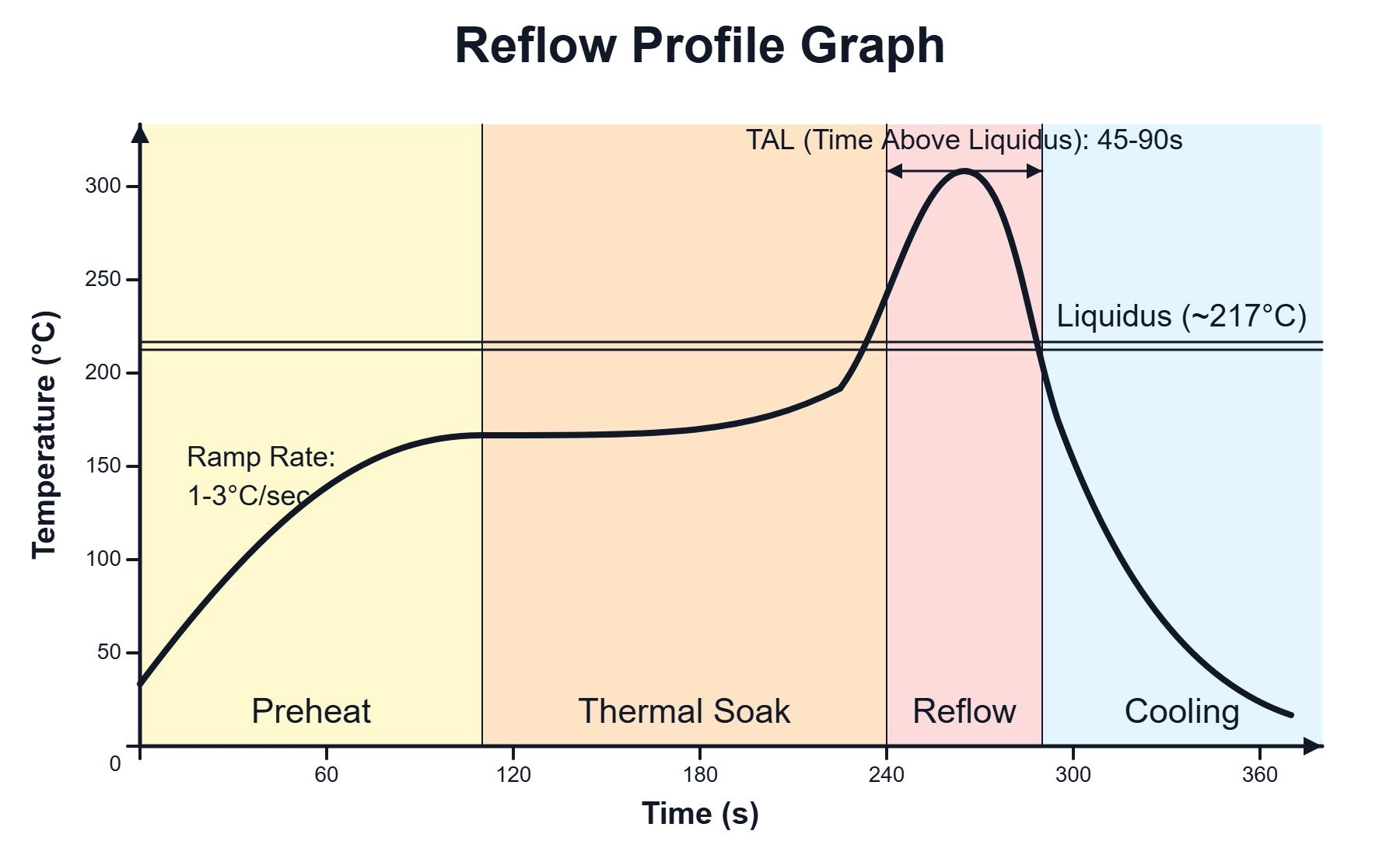
Figure: Reflow profile graph showing the Time versus Temperature curve across the Preheat, Thermal Soak, Reflow, and Cooling stages of SMT assembly.
Preheat Stage
The preheat stage safely transitions the board from ambient temperature to around 150°C. The critical metric here is the ramp rate, which must be strictly controlled to 1.0–3.0°C per second. Why?
If the ramp is too aggressive, the volatile solvents in the solder paste will boil rapidly, causing paste splattering (solder balls) and thermal shock to ceramic capacitors.
Soak Stage
The thermal soak phase holds the board in a thermal equilibrium, typically between 150°C and 200°C for 60 to 120 seconds. Why?
This stage has two purposes. First, it ensures that high thermal mass components (like heavy inductors) and low thermal mass components (like 0402 resistors) reach the same temperature before melting begins. Second, it activates the flux chemistry to chemically reduce surface oxides on both the PCB pads and component leads.
Reflow (Peak Temperature) Stage
This is the phase where the solder alloy transitions into a liquid. The reflow soldering temperature profile enters the critical Time Above Liquidus (TAL) zone. For 45 to 90 seconds, the temperature peaks roughly 20–30°C above the alloy's melting point. Why?
This ensures thorough wetting of the pads and drives the formation of a strong intermetallic layer between the copper and the solder.
Cooling Stage
The cooling stage brings the liquid solder back to a solid state using a controlled downward slope of -2°C to -4°C per second. Why? A rapid, controlled cool-down promotes a fine-grained, mechanically robust solder joint. If cooling is too slow, the joint becomes grainy and brittle. If it is too fast (e.g., > -6°C/sec), the sudden contraction can fracture delicate components.
Reflow Soldering Temperature Curve Explained
A typical reflow profile graph shows the relationship between temperature and time as the PCB travels through each oven zone.
Typical Temperature Range for Lead-Free Solder
Modern manufacturing relies almost exclusively on SAC305 (Sn96.5/Ag3.0/Cu0.5) alloys. A reflow soldering profile lead-free setup requires significantly higher heat than traditional tin-lead pastes. The melting point of SAC305 is ~217°C, meaning the peak oven temperature must hit 240°C-250°C to achieve proper wetting, reducing the margin of error before damaging components.
Ramp Rate and Thermal Gradient
A steep thermal gradient across a PCB is disastrous. Multi-layer PCBs contain varying densities of copper. If the ramp rate is uneven or too fast, the outer layers expand faster than the inner layers, leading to structural delamination or via barrel cracking.
Conversely, if the ramp rate through the soak zone is too slow or too hot, you risk flux exhaustion. The active chemicals burn off before the alloy reaches liquidus, leaving the metal exposed to re-oxidation right before the critical melting phase.
Peak Temperature and Time Above Liquidus
Peak temperature and TAL selection are governed by metallurgical kinetics. Why should TAL not exceed 90 seconds? Solder does not simply stick to a copper pad; it forms an Intermetallic Compound (IMC), specifically Cu3Sn and Cu6Sn5 layers.
A healthy IMC layer (1-3 microns) is necessary for a mechanical bond. However, if TAL extends to 110 seconds or beyond, the IMC layer grows excessively thick. Because IMCs are inherently brittle, a thick layer creates a fragile joint prone to sheer failure under physical vibration. Furthermore, prolonged liquidus causes copper dissolution kinetics - the aggressive SAC alloy literally dissolves the copper trace into the solder matrix, eating away the pad.
How to Create an Optimal Reflow Profile
Developing an engineering-grade profile requires a systematic, procedural approach. Here is the process manual for dialing in a new PCB assembly:
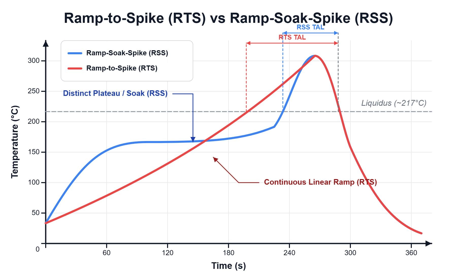
Figure: Comparison graph illustrating the thermal curve differences between a linear Ramp-to-Spike (RTS) profile and a plateaued Ramp-Soak-Spike (RSS) profile.
Step 1: Read the Paste Datasheet
Start by defining your absolute thermal boundaries. Decide between a Ramp-to-Spike (RTS) or Ramp-Soak-Spike (RSS) curve.
- RTS is preferred for simple boards with uniform thermal mass; it minimizes heat exposure.
- RSS is mandatory for complex boards to allow heavy components to "catch up" in temperature during the soak phase.
Step 2: Define Peak Temperature Limits
Identify the most heat-sensitive component on your Bill of Materials (BOM) to ensure your peak temperature does not exceed its maximum rating (often 260°C for 10 seconds for standard plastic connectors or ICs).
Step 3: Set Initial Zone Temperatures
Input baseline temperatures into your oven software. For an 8-zone oven running SAC305, a starting theoretical table might look like this:
Zone Number | Purpose | Top Temp (°C) | Bottom Temp (°C) |
|---|---|---|---|
Zones 1–3 | Preheat | 120 / 140 / 160 | 120 / 140 / 160 |
Zones 4–5 | Soak | 180 / 190 | 180 / 190 |
Zone 6 | Pre-Reflow | 210 | 210 |
Zone 7 | Peak Reflow | 255 | 255 |
Zone 8 | Cooling | Air Chill | Air Chill |
Step 4: Calculate Conveyor Speed
The physical length of the oven divided by the desired total profile time dictates your conveyor speed. If an oven's heated length is 300cm and the paste requires a 4-minute profile, the baseline speed is 75 cm/minute.
Step 5: Run a Profiling Board
Attach K-type thermocouples to a fully populated "dummy" board.
Step 6: Execute ΔT Correction
Analyze the profiler data. Your goal is to keep the delta (ΔT) between the hottest and coldest components under 10°C during reflow.
If a heavy inductor is peaking at 230°C (too cold) while a 0402 resistor hits 255°C (too hot): Increase the Soak Time to allow the inductor to absorb more heat before entering the peak zone, rather than just blasting the peak temperature higher. In real production environments, achieving a stable profile often requires multiple profiling iterations, particularly when switching PCB stackups, copper weights, or component densities.
Common Reflow Profile Problems
Process engineering relies on connecting the physical defect directly to a temperature mistake.
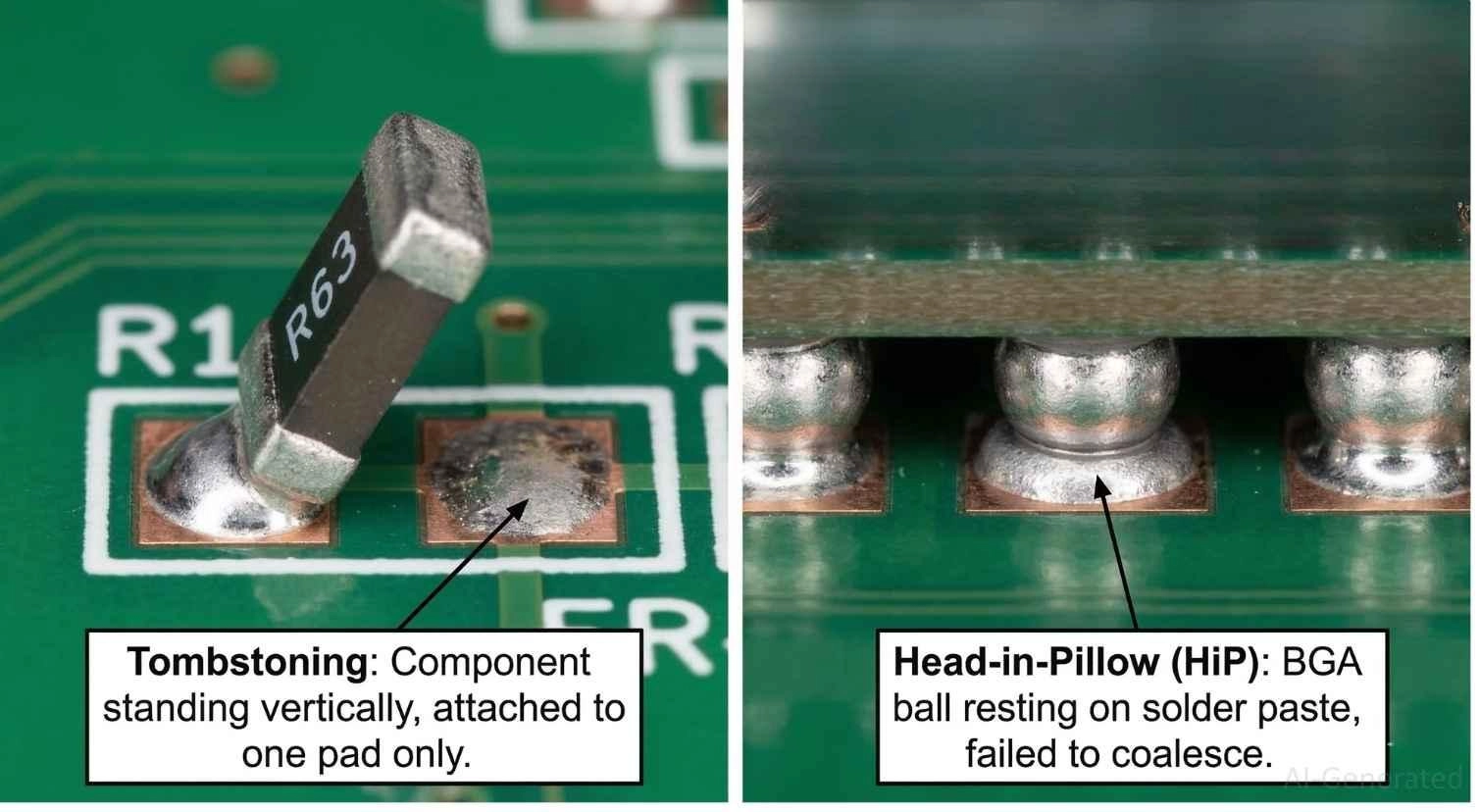
Figure: SMT soldering defects: Tombstoning of a passive component and Head-in-Pillow failure under a BGA package.
Tombstoning
- The Defect: One end of a passive component lifts off the pad, standing upright like a tombstone.
- The Cause & Fix: The ramp rate entering the reflow stage is too fast. The solder paste on one pad reaches the liquidus and wets before the other pad. Fix: Slow down the ramp rate or switch to an RSS profile to ensure both pads cross the liquidus threshold simultaneously.
Head-in-Pillow (HiP)
- The Defect: The solder ball of a BGA rests on the solder paste deposit but fails to coalesce, looking like a head resting on a pillow.
- The Cause & Fix: Usually caused by early flux exhaustion or dynamic PCB warpage during the peak stage. Fix: Shorten the soak duration to preserve flux activity, or reduce the peak temperature slightly to prevent the BGA package from warping upward.
Solder Voids
- The Defect: Pockets of trapped outgassing (bubbles) inside the solid solder joint, weakening thermal and electrical conductivity.
- The Cause & Fix: The soak stage was insufficient. The flux solvents did not fully evaporate before the exterior of the solder joint hardened. Fix: Extend the soak time to allow complete outgassing before liquidus.
Component Cracking & PCB Warpage
- The Defect: Micro-cracks in ceramic capacitors, or a permanently bowed FR4 substrate.
- The Cause & Fix: A cooling slope exceeding -4°C/sec causes thermal shock (cracking). A severe mismatch between top and bottom oven zone temperatures causes warpage. Fix: Flatten the cooling slope and balance the convection blowers evenly between the top and bottom zones.
Reflow Profile Differences: Lead-Free vs Leaded Solder
Temperature Differences
Leaded solder (Sn63/Pb37) boasts a highly forgiving melting point of 183°C, allowing for a safe peak temperature of ~210–220°C. Conversely, Lead-free (SAC305) melts at 217°C, requiring a peak of ~240–250°C.
Process Adjustments
Because lead-free pastes require higher heat, the process window is dramatically narrower. The process window represents the allowable temperature and time tolerance where acceptable solder joints are consistently produced. A narrow process window in lead-free assembly requires tighter oven control and frequent profiling verification. You have less than a 15°C buffer between a successful lead-free melt and the thermal destruction of standard FR4 substrates and plastic component bodies.
Reliability Considerations
Lead-free profiles put immense thermal stress on the assembly. As discussed earlier, the higher temperatures vastly accelerate copper dissolution, making the precise management of TAL even more critical for lead-free assemblies than it was in the legacy tin-lead era.
Equipment Used for Reflow Soldering
Reflow Ovens
Industrial manufacturing relies on multi-zone forced convection reflow ovens. While some hobbyists attempt reflow soldering at home using modified toaster ovens, these lack closed-loop zone control and even air distribution, making repeatable SAC305 soldering incredibly difficult.
Temperature Profiling Tools
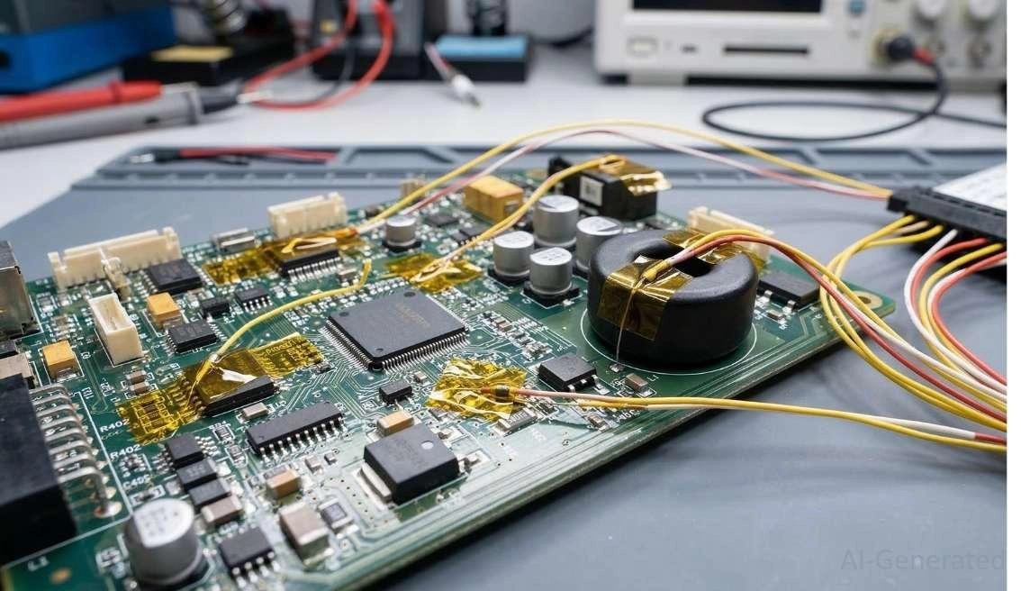
Figure: A test PCB prepared for thermal profiling, showing K-type thermocouples attached to high and low thermal mass components using Kapton tape.
Profilers are data-logging devices that travel through the oven alongside the PCB. To gather actionable data, engineers typically use 4 to 6 thermocouples adhered with high-temperature Kapton tape or thermal epoxy.
Placement Strategy:
- 1 probe on the largest thermal mass (e.g., a power inductor).
- 1 probe on the lowest thermal mass (e.g., a 0402 resistor).
- 1 probe directly on the body of a heat-sensitive IC or plastic connector.
- 1 probe on a bare FR4 spot to measure substrate stress.
By reading the convergence of these lines on the software graph, engineers can isolate the exact zone where thermal divergence occurs.
Advanced PCB Assembly with Optimized Reflow Profiles at JLCPCB
Achieving high-yield production requires mastering mixed-SMD optimization. When a PCB features massive thermal imbalances - such as a large copper plane acting as a massive heat sink beneath a power MOSFET, situated next to tiny 0201 passives - standard profiles fail.
To protect delicate components while ensuring heavy thermal masses reach liquidus, engineers must employ selective shielding methods, specialized reflow pallets, or local thermal buffering. Additionally, proper copper balancing in PCB design is essential to minimize uneven heat sinking.
Advanced manufacturers must utilize Nitrogen (N2) convection. Pumping nitrogen into the reflow chamber displaces oxygen, practically eliminating high-temperature oxidation. This vastly widens the process window, allowing for better wetting at slightly lower peak temperatures, saving heat-sensitive components.
Furthermore, managing double-sided reflow requires strict zone-by-zone tuning to ensure bottom-side components (soldered during the first pass) do not exceed their liquidus point and drop off the board during the second pass.
To combat these extreme engineering challenges, JLCPCB utilizes state-of-the-art, multi-zone industrial nitrogen convection ovens. By utilizing extended multi-zone profiling, our engineers flatten the thermal gradient, ensuring massive connectors reach reflow temperature without scorching adjacent micro-components.
For engineers demanding industrial-grade process control, explore JLCPCB's PCB Assembly services. You can instantly check automated production costs via our Quotation Page.
Best Practices for Reflow Soldering Profiles
Monitoring Temperature Profiles
Profile creation is not a "set and forget" task. Engineers should run continuous profiling validation using a dedicated "golden board" (a fully populated test board reserved only for profiling) at the start of every production shift or whenever changing product runs.
Maintaining Reflow Oven Calibration
Schedule routine oven calibration. Over time, blower motors degrade, and heating elements drift, meaning the physical zone temperature may no longer match the software setpoint.
Material Handling Protocols
Even the perfect profile will fail if the paste is mishandled. Maintain strict paste storage protocols - keep refrigerated until use, then allow it to thaw completely to room temperature naturally before opening to prevent condensation from introducing moisture into the flux. Additionally, ensure consistent board loading gaps on the conveyor to prevent air-flow starvation inside the oven.
FAQ About Reflow Soldering Profiles
Q: How many times can a standard PCB safely pass through a reflow oven?
Typically, a standard FR4 board can withstand up to three full thermal excursions (e.g., top side, bottom side, and one potential rework cycle). Exceeding this limit severely degrades the FR4 substrate and creates dangerously thick intermetallic compound (IMC) layers, resulting in brittle joints.
Q: Do I need to pre-bake my components before subjecting them to a reflow profile?
Yes, if your components are rated as Moisture Sensitive Devices (MSDs) and have exceeded their allowable factory floor life. If unbaked, the rapid temperature climb during the preheat and reflow stages will cause trapped moisture to boil instantly, cracking the component package - a defect known as the "popcorn effect."
Q: Can I use a lead-free reflow profile if some of my components have legacy leaded finishes?
Mixing alloys is highly discouraged in professional SMT assembly. Subjecting a legacy leaded component to a 250°C lead-free peak can easily destroy its plastic housing or internal die. Additionally, the mixed metallurgy creates unpredictable, structurally compromised solder joints with altered, uneven melting points.
Q: How does the PCB substrate thickness alter the required soak time?
Thicker substrates (e.g., 2.4mm or 3.2mm backplanes) act as massive thermal sinks compared to standard 1.6mm boards. They require a significantly extended soak phase to ensure the dense inner copper planes achieve thermal equilibrium with the outer surface pads before the board enters the liquidus stage.
Q: Can I use external fans to speed up the cooling stage?
No. Forcing a rapid cool-down (exceeding -4°C/sec) using uncalibrated external fans induces severe thermal shock across the PCB. This sudden contraction can shear the pads off the board, fracture delicate ceramic capacitors (MLCCs), and create microscopic stress fractures within the solder joints. The cooling slope must be exclusively controlled by the oven's designated cooling zones.
Conclusion
Mastering the reflow soldering profile is the cornerstone of high-yield electronics manufacturing. By understanding the physics of the ramp, soak, peak, and cooling stages, process engineers can directly eliminate defects ranging from Head-in-Pillow to aggressive copper dissolution. Success requires meticulously matching the thermal curve to the solder paste datasheet, profiling for $\Delta$T correction, and respecting the PCB's unique thermal mass distribution.
When you are ready to put theory into production, ensure you are starting with top-tier materials.
Source reliable, authentic components for your SMT process at the JLCPCB Parts Page, and bring your optimized designs to life seamlessly at JLCPCB.
Popular Articles
• Common PCB Assembly Methods and Soldering Techniques Explained
• What Is BGA Void? Causes, IPC Limits, and Solutions
• SMD Soldering Tools You Need: Complete Guide from Beginner to Pro
• Reflow Soldering: Everything You Need to Know
• SMT Assembly Process Explained and Equipment Used: A Step-by-Step Guide to PCBA Manufacturing
Keep Learning
12 Professional Soldering Tips and Tricks Every Beginner Should Know
Soldering is not merely "gluing" metal; it is a metallurgical process that creates an intermetallic compound (IMC). This molecular bond ensures the electrical and mechanical integrity of your device. A poor joint might pass a quick visual check but will inevitably fail under vibration or thermal stress, leading to "ghost" bugs and hardware failures. These soldering tips and tricks focus on practical, repeatable techniques used in professional electronics soldering—from correct heat transfer and flux u......
Solder Melting Point Guide: Chart, Alloy Types, and Reflow Considerations
In the precise world of electronics manufacturing, a difference of just a few degrees can mean the distinction between a perfect, reliable solder joint and a catastrophic "cold" joint failure. While many hobbyists view soldering simply as "melting metal to stick things together," professional PCB assembly requires a nuanced understanding of thermodynamics. The solder melting point is not simply a single value listed in a datasheet; it is a decisive limit that determines the choice of components, the s......
The Ultimate Guide to Solder Flux: Everything You Should Know Before Soldering PCB
Soldering is needed to make almost all electronic devices. Adding solder alone won't make a joint that is strong, clean, and sound from a metallurgical point of view. Solder flux is a very important part of the process that comes in here. If you want to do your job better and make it more reliable, you need to know a lot about soldering flux, whether you're an engineer, a professional technician, or just a hobbyist. This article goes into a lot of detail about solder flux, including what it is, how it......
Common PCB Assembly Methods and Soldering Techniques Explained
Whether you're designing your first prototype or scaling up to production, understanding PCB assembly methods and soldering techniques is crucial to achieving reliable, high-performance circuit boards. Modern PCBA primarily relies on Surface Mount Technology (SMT) and Through-Hole Technology (THT)—each offering unique advantages for component density, durability, and manufacturability. In this guide, we'll break down the major PCB assembly methods, key soldering techniques such as reflow and wave sold......
Flex PCB Assembly Guide: Process, Challenges, and Solutions
Flexible Printed Circuit Boards (Flex PCBs) are the foundational technology enabling the compact, innovative design of modern electronics. Because of their ability to bend and fold, they power devices from smart wearables to compact medical instruments where traditional rigid printed circuit boards (Rigid PCBs) can't be used. Achieving a functional electronic circuit from the raw plastic film demands special expertise, with flexible PCB assembly (FPCA) representing the crucial final step in this trans......
SMD Rework Guide: Tools, Temperatures, and Techniques That Prevent PCB Damage
From replacing a burned regulator to correcting wrong component values or removing solder bridges on fine-pitch ICs, SMD rework is an essential skill in electronics manufacturing and prototyping. It allows engineers to repair assembly defects, implement design changes, and recover valuable PCBs without the cost and delay of building new boards. In this guide, you will learn: What SMD rework is Common rework scenarios Tools and temperatures Safe removal and installation Package-specific techniques Real......