
What Is BGA Void? Causes, IPC Limits, and Solutions
11 min
- What Is BGA Voiding and How Does It Form in Solder Joints?
- Common Root Causes of BGA Voiding in PCB Assembly
- Types and Classification of BGA Voids
- IPC Standards for Acceptable BGA Voiding Levels
- How to Reduce and Prevent BGA Voiding: Proven Solutions
- How JLCPCB Controls BGA Voiding in Mass Production
- X-Ray Inspection (AXI) for BGA Voiding Detection and Analysis
- FAQs About BGA Voiding
- Conclusion
In the high-stakes world of SMT (Surface Mount Technology), the Ball Grid Array (BGA) is a critical component for modern high-density electronics. However, it introduces a complex challenge: the BGA void. While analysis is important, the ultimate goal for any PCB designer or manufacturer is prevention.
Unlike visible solder joints, BGA connections are hidden. A void - a gas bubble trapped within the hardened solder - can compromise thermal conductivity and mechanical integrity.
At JLCPCB, we prioritize void mitigation through strict adherence to IPC standards, advanced DFM checks, and precise reflow profiling. This guide focuses on actionable strategies to achieve near-zero voiding.
What Is BGA Voiding and How Does It Form in Solder Joints?
At its core, a BGA void is a cavity formed within the solder joint. It occurs when volatile compounds (from flux or circuit board moisture) turn into gas during the reflow process but fail to escape before the solder solidifies.
When the solder paste melts, the flux vehicle creates gases as it cleans the metal surfaces. In a perfect scenario, these bubbles rise to the surface and dissipate due to buoyancy. However, if the surface tension of the molten solder is too high, or if the cooling phase begins too quickly, the gas becomes trapped, effectively freezing a bubble inside the metal joint.
Technical Note
The physics of void formation is a battle between buoyancy force (pushing gas out) and viscous drag/surface tension (keeping gas in).
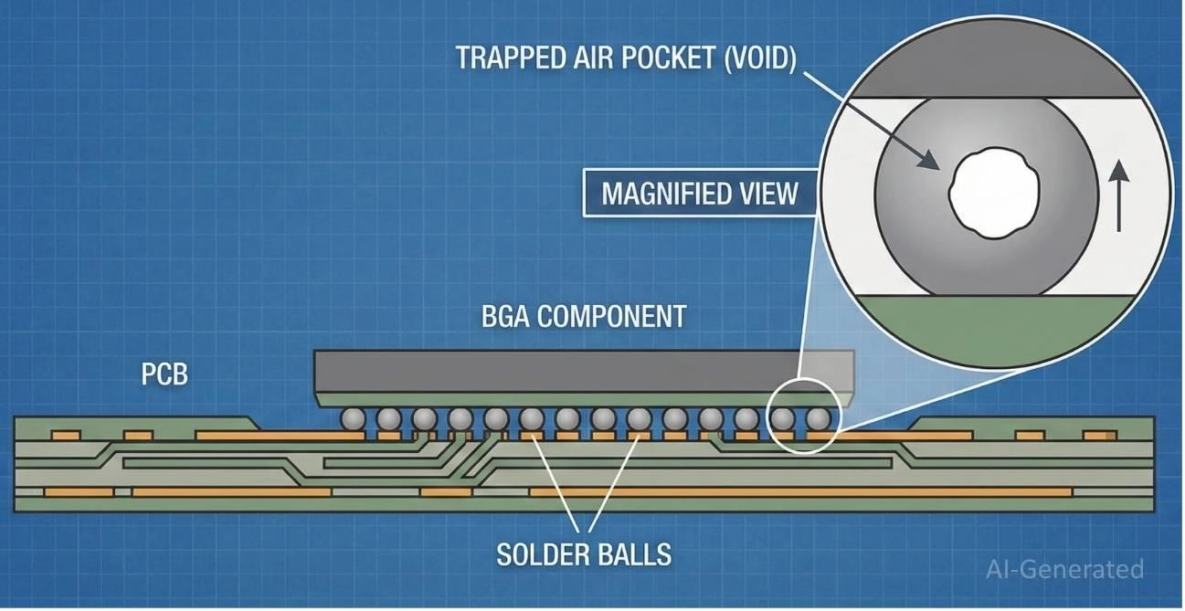
Figure: A BGA void trapped inside a solder ball due to flux outgassing during SMT reflow.
Common Root Causes of BGA Voiding in PCB Assembly
To reduce voids, we must first understand where they come from. About 90% of voiding issues stem from four specific areas.
Cause 1: Solder Paste Chemistry and Flux Volatiles
The type of solder paste used is the primary contributor. Pastes are a mixture of metal alloy spheres and flux vehicle.
● High Volatile Content: Fluxes designed for high wettability often contain more volatile solvents. If these solvents do not fully evaporate during the "soak" phase of reflow, they will boil violently during the "reflow" phase, creating large voids.
● Lead-Free Alloys: SAC305 and other lead-free alloys have higher surface tension than traditional SnPb solder, making it harder for gas bubbles to escape.
Cause 2: Improper Reflow Thermal Profile
The temperature curve your board travels through inside the reflow oven is critical.
● Short Soak Time: The "Soak Zone" (typically 150°C to 190°C) is where volatiles should burn off. If this stage is too short, gas remains trapped.
● Short Time Above Liquidus (TAL): If the solder stays molten for too short a time, the bubbles don't have enough time to rise to the surface and pop.
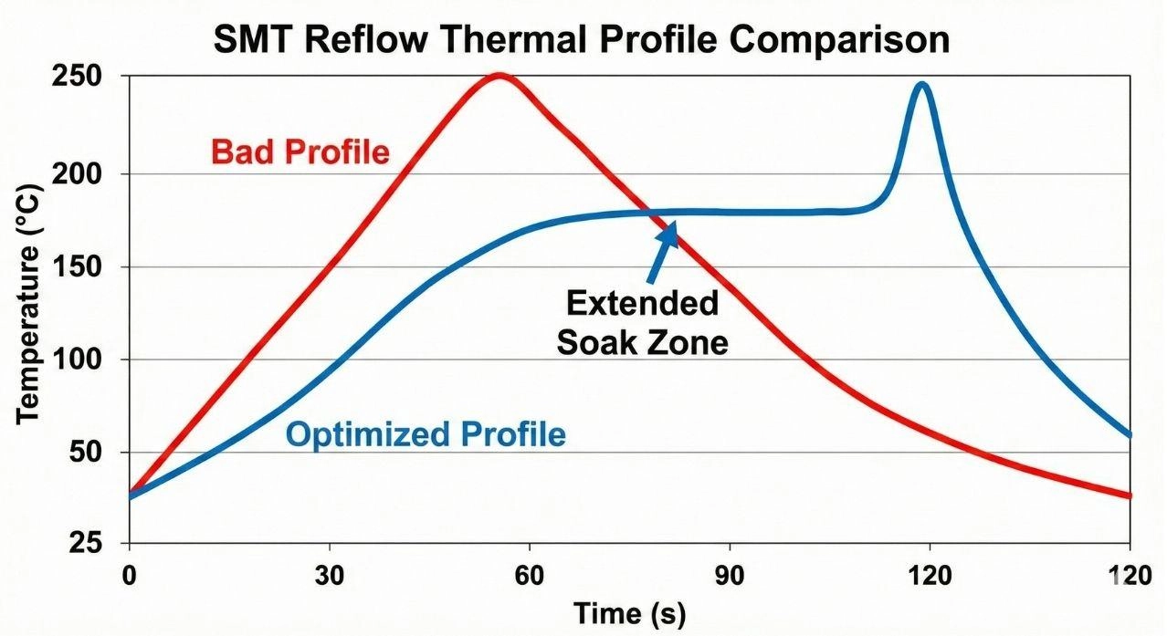
Figure: SMT reflow thermal profiles showing an extended soak zone to reduce BGA voiding.
Cause 3: PCB Pad Design and Via-in-Pad Defects
This is a frequent issue seen in Gerber files uploaded to JLCPCB.
● Open Via-in-Pad: If a via is placed directly in the BGA pad without being plugged or tented, air travels up from the bottom of the board through the via like a chimney. This air blasts into the molten solder ball, creating massive voids.
Check our "Via-in-Pad" capabilities to see how we handle filled vias for high-density designs.
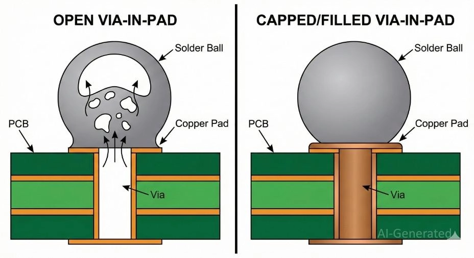
Figure: Showing how open via-in-pad designs cause massive BGA voids versus filled via-in-pad technology.
Cause 4: Stencil Aperture and Printing Issues
If the SMT stencil deposits too much paste, the excessive flux volume generates more gas than can escape. Conversely, a 1:1 circular aperture often traps air in the corners during printing.
Types and Classification of BGA Voids
Not all voids are created equal. Identifying the "species" of void helps in troubleshooting the root cause.
1. Macro Voids (Process Voids): The most common type, caused by trapped flux gases. These are usually random and float in the upper half of the solder ball.
2. Planar Microvoids: These are small, dangerous voids located right at the interface between the solder and the pad. They are often caused by surface finish issues (like Black Pad in ENIG) and can lead to catastrophic "head-in-pillow" failures.
3. Shrinkage Voids: These look like jagged cracks rather than smooth bubbles. They form during the cooling phase when the exterior of the ball hardens before the interior, creating a vacuum cavity as the metal shrinks.
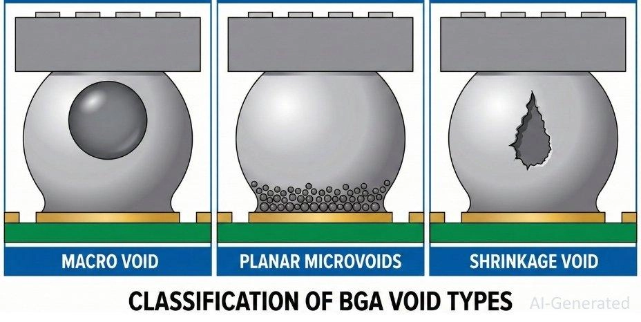
Figure: BGA void types: Macro Voids, Planar Microvoids, and Shrinkage Voids.
IPC Standards for Acceptable BGA Voiding Levels
It is important to note that not all voids are failures. In fact, small voids can sometimes arrest crack propagation. However, reliability depends on the size and location of the void.
The industry standard governing this is IPC-7095 (Design and Assembly Process Implementation for BGAs).
| Class | Product Type | Acceptable Void Criteria (Area %) |
|---|---|---|
| Class 1 | General Consumer Electronics | < 60% void area diameter |
| Class 2 | Dedicated Service Electronics | < 25% cumulative void area |
| Class 3 | High Reliability (Medical/Aero) | < 25% cumulative void area (Stricter process control) |
How to Reduce and Prevent BGA Voiding: Proven Solutions
If you are designing a board for manufacturing (DFM) or setting up a process, here is how to keep voiding under 25%.
1. Reflow Profile Optimization
The "Ramp-to-Spike" profile is often inferior to a "Ramp-Soak-Spike" profile for BGA assembly.
● Extend the Soak: increasing the soak time (60–90 seconds) allows the flux solvents to outgas before the alloy melts.
● Control the Cooling: A controlled cooling rate prevents shrinkage voids.
2. Stencil Design Optimization
Instead of a standard circular aperture for BGA pads, consider using a "Window Pane" or "Home Plate" design.
● Window Pane: Breaking a large aperture into four smaller squares reduces total paste volume and provides channels for gas to escape.
Order high-precision electropolished stencils from JLCPCB to ensure perfect paste release.
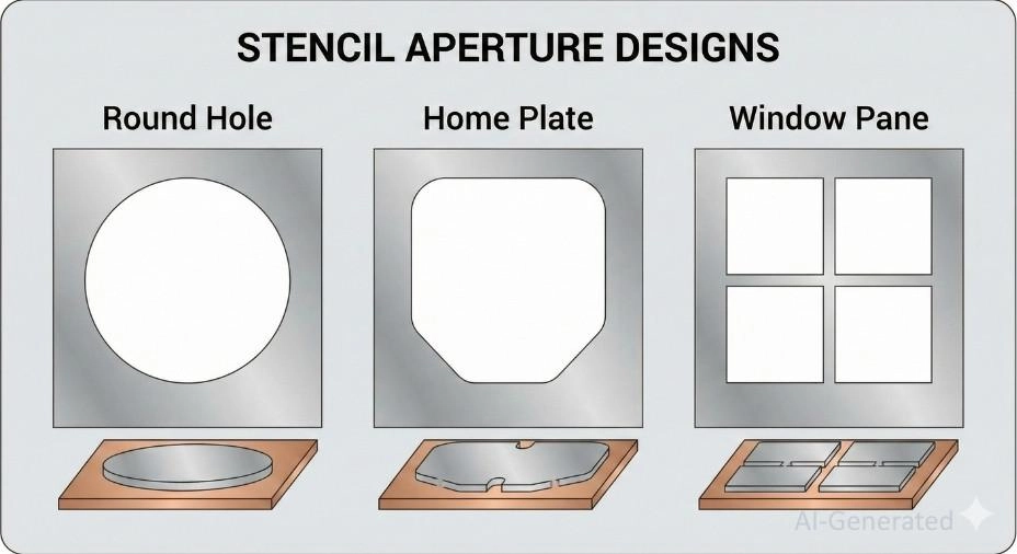
Figure: Stencil aperture designs for BGA pads, including Home Plate and Window Pane to allow gas escape and reduce voiding.
3. Low-Voiding Solder Paste Selection
Switching to a solder paste specifically formulated for "Low Voiding" can yield immediate results. These pastes often use specific activators that degas at lower temperatures.
Note
Beyond standard process settings, here are specific practical tips for PCB designers and assembly technicians to minimize void risks before the board even hits the line.
4. Choose NSMD (Non-Solder Mask Defined) Pads for Better Wetting
Where possible, use NSMD pads. In NSMD designs, the solder mask opening is larger than the copper pad. This provides a small gap around the pad that allows gas to escape more easily compared to SMD (Solder Mask Defined) pads, where the mask overlaps the copper. NSMD pads also provide better stress relief for the solder joint.
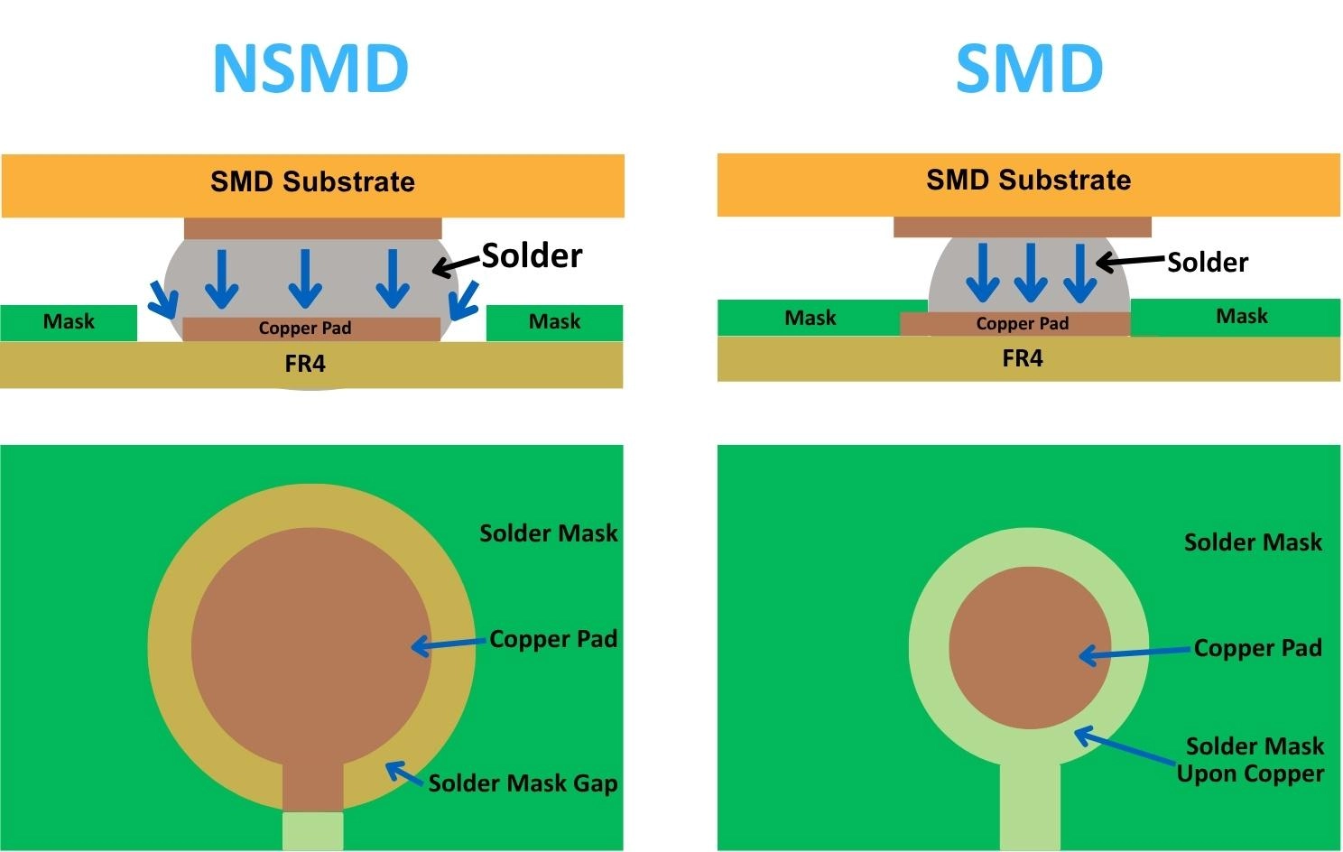
Figure: Difference of soldering in SMD vs NSMD
5. Control Proper Moisture Sensitivity Level (MSL) and Component Baking
Moisture trapped inside the BGA package or PCB substrate turns into steam during reflow, contributing to voiding.
● Practical Tip: Always bake BGA components according to J-STD-033 standards before assembly if they have been exposed to humidity. JLCPCB follows strict storage protocols to ensure components are dry before mounting.
6. Use POFV (Plated Over Filled Via) for Via-in-Pad Designs
If your design requires placing vias directly under BGA balls (common in 0.4mm pitch parts), you must use POFV technology.
● The Risk: Standard tenting with solder mask is insufficient; air will burst through the mask.
● The Solution: JLCPCB's POFV process fills the via with epoxy resin and plates copper over it, creating a flat, air-tight surface that eliminates via-induced voiding.
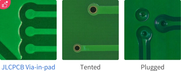
Figure: JLCPCB Via-in-pad vs Tented and Plugged via
7. Proper Solder Paste Handling
Ensure solder paste is allowed to reach room temperature naturally before opening the jar. Opening cold paste introduces condensation (water), which is a primary source of voids.
How JLCPCB Controls BGA Voiding in Mass Production
Handling BGAs requires a synergy of advanced equipment and experienced engineering.
● Precision: We support fine-pitch BGAs down to 0.35mm.
● Verification: X-Ray inspection is a standard procedure, not an expensive add-on.
● Efficiency: Our smart factories optimize reflow profiles based on your specific BOM and PCB thickness.
Learn More: JLCPCB PCB Assembly Capabilities
X-Ray Inspection (AXI) for BGA Voiding Detection and Analysis
Because BGA joints are sandwiched between the component and the PCB, visual inspection (AOI) is useless. You cannot see the voids with the naked eye.
This is why Automated X-Ray Inspection (AXI) is mandatory for reliable BGA assembly. X-rays penetrate the silicon and FR4 material but are blocked by the lead/tin alloy. On an X-ray image, the solder ball appears dark, while the void appears as a lighter, brighter spot within the ball.
At JLCPCB, we utilize high-resolution X-ray inspection for all PCBA orders containing BGA parts. Our Quality Assurance (QA) engineers measure the void percentage against IPC standards. If a board exceeds the safety threshold, it is flagged for rework or rejection before it ever ships to you.
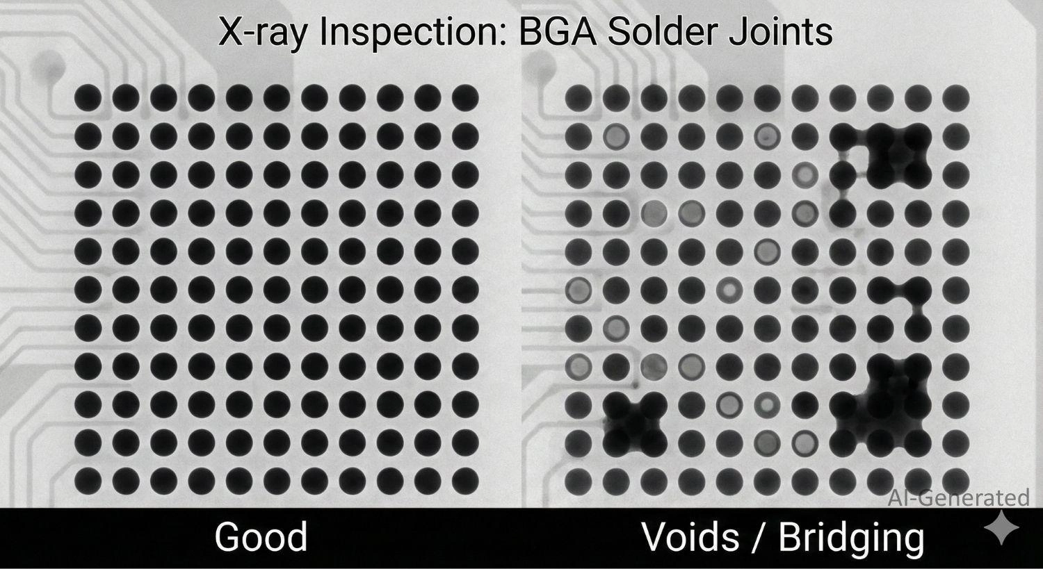
Figure: 2D X-ray inspection image showing BGA void detection in a ball grid array assembly.
FAQs About BGA Voiding
Q1. Is it possible to achieve 0% BGA voiding?
In a practical manufacturing environment, achieving 0% voiding across an entire BGA component is extremely difficult due to the physics of flux outgassing. Even IPC Class 3 standards (High Reliability) allow for some voiding (up to 25% area). The goal is not total elimination, but controlling the size and location of voids to ensure they do not affect mechanical or electrical integrity.
Q2. Do baking components remove BGA voids?
Baking components before assembly (MSL control) removes moisture from the package, which prevents "popcorning" (cracking of the component body). While this eliminates moisture-induced steam bubbles, it does not prevent voids caused by solder paste flux outgassing. Both proper component storage and correct reflow profiling are needed.
Q3. Can BGA voids be repaired after assembly?
Yes, but it is an invasive process. If X-ray inspection detects excessive voiding, the entire BGA component must be desoldered using a hot-air rework station, the site cleaned (dressed), and a new component resoldered. Repeated rework can thermally stress the PCB pads, so getting it right the first time via JLCPCB's controlled process is preferred.
Q4. Why are Lead-Free (RoHS) builds more prone to voiding?
Lead-free solder alloys (like SAC305) have higher surface tension and require higher reflow temperatures than traditional Tin-Lead solders. The higher surface tension makes it harder for gas bubbles to break free from the molten metal, trapping them inside. Additionally, the higher heat required can cause flux to volatize more aggressively.
Q5. How does the PCB surface finish affect voiding?
The flatness and oxidation level of the pad matter. ENIG (Electroless Nickel Immersion Gold) is generally preferred for BGAs because it is perfectly flat. However, if the Gold/Nickel interface is compromised (Black Pad), it can cause planar microvoids. HASL (Hot Air Solder Leveling) is less flat, which can cause uneven paste printing, indirectly leading to voids.
Q6: How Much BGA Voiding Is Too Much?
For most applications, BGA voiding should be kept below 25% of the solder joint area, according to industry-accepted standards from IPC.
Q7: Why BGA Reballing Often Fails in Field Repairs?
BGA reballing in the field often fails because standard repair shops lack the precise thermal profile and X-Ray inspection used in factories. Without uniform heating, the circuit board often warps, preventing the hundreds of microscopic solder balls from making consistent contact.
Additionally, trapped moisture can cause the chip to crack internally (the "popcorn effect") during the reflow process. Ultimately, these "blind" repairs cannot guarantee the sub-micron alignment required for long-term reliability.
Conclusion
BGA void prevention is a holistic approach combining Design (DFM), Process (Profile), and Materials (Paste). By implementing these strategies - optimizing your reflow profile, selecting the right paste, using POFV technology, and following strict handling protocols - you can drastically reduce the risk of field failures.
Popular Articles
• Common PCB Assembly Methods and Soldering Techniques Explained
• What Is BGA Void? Causes, IPC Limits, and Solutions
• SMD Soldering Tools You Need: Complete Guide from Beginner to Pro
• Reflow Soldering: Everything You Need to Know
• SMT Assembly Process Explained and Equipment Used: A Step-by-Step Guide to PCBA Manufacturing
Keep Learning
Common PCB Assembly Methods and Soldering Techniques Explained
Whether you're designing your first prototype or scaling up to production, understanding PCB assembly methods and soldering techniques is crucial to achieving reliable, high-performance circuit boards. Modern PCBA primarily relies on Surface Mount Technology (SMT) and Through-Hole Technology (THT)—each offering unique advantages for component density, durability, and manufacturability. In this guide, we'll break down the major PCB assembly methods, key soldering techniques such as reflow and wave sold......
12 Professional Soldering Tips and Tricks Every Beginner Should Know
Soldering is not merely "gluing" metal; it is a metallurgical process that creates an intermetallic compound (IMC). This molecular bond ensures the electrical and mechanical integrity of your device. A poor joint might pass a quick visual check but will inevitably fail under vibration or thermal stress, leading to "ghost" bugs and hardware failures. These soldering tips and tricks focus on practical, repeatable techniques used in professional electronics soldering—from correct heat transfer and flux u......
Solder Melting Point Guide: Chart, Alloy Types, and Reflow Considerations
In the precise world of electronics manufacturing, a difference of just a few degrees can mean the distinction between a perfect, reliable solder joint and a catastrophic "cold" joint failure. While many hobbyists view soldering simply as "melting metal to stick things together," professional PCB assembly requires a nuanced understanding of thermodynamics. The solder melting point is not simply a single value listed in a datasheet; it is a decisive limit that determines the choice of components, the s......
The Ultimate Guide to Solder Flux: Everything You Should Know Before Soldering PCB
Soldering is needed to make almost all electronic devices. Adding solder alone won't make a joint that is strong, clean, and sound from a metallurgical point of view. Solder flux is a very important part of the process that comes in here. If you want to do your job better and make it more reliable, you need to know a lot about soldering flux, whether you're an engineer, a professional technician, or just a hobbyist. This article goes into a lot of detail about solder flux, including what it is, how it......
Flex PCB Assembly Guide: Process, Challenges, and Solutions
Flexible Printed Circuit Boards (Flex PCBs) are the foundational technology enabling the compact, innovative design of modern electronics. Because of their ability to bend and fold, they power devices from smart wearables to compact medical instruments where traditional rigid printed circuit boards (Rigid PCBs) can't be used. Achieving a functional electronic circuit from the raw plastic film demands special expertise, with flexible PCB assembly (FPCA) representing the crucial final step in this trans......
SMD Rework Guide: Tools, Temperatures, and Techniques That Prevent PCB Damage
From replacing a burned regulator to correcting wrong component values or removing solder bridges on fine-pitch ICs, SMD rework is an essential skill in electronics manufacturing and prototyping. It allows engineers to repair assembly defects, implement design changes, and recover valuable PCBs without the cost and delay of building new boards. In this guide, you will learn: What SMD rework is Common rework scenarios Tools and temperatures Safe removal and installation Package-specific techniques Real......