
PCB X-Ray Inspection Explained: Non-Destructive Testing for PCB Assembly Quality Control
14 min
- What Is PCB X-Ray Inspection?
- Why X-Ray Inspection Is Essential for Modern PCBs
- How PCB X-Ray Inspection Works
- PCB Components That Require X-Ray Inspection
- Common Defects Detected by PCB X-Ray Inspection
- PCB X-Ray Inspection vs Other Inspection Methods
- IPC Standards and Acceptance Criteria for X-Ray Inspection
- Limitations of PCB X-Ray Inspection
- Technical Specifications and Selection Criteria for SMT X-Ray Inspection
- Choosing a PCB Assembly Manufacturer with X-Ray Capability
- Future Trends in X-Ray Inspection Technology
- FAQ about PCB X-Ray Inspection
- Conclusion: Is PCB X-Ray Inspection Necessary for Your Project?
In the era of miniaturization, modern printed circuit boards (PCBs) face an invisible challenge: verifying the quality of solder joints hidden beneath components. With Ball Grid Array (BGA) packages featuring pitch sizes down to 0.3mm and Quad Flat No-lead (QFN) components concealing critical thermal connections, traditional optical methods are blind to the most critical failure points.
PCB X-ray inspection has emerged as the definitive solution. This guide explores the technical foundations, applications, and acceptance criteria of X-ray inspection, empowering engineers to ensure manufacturing reliability.
What Is PCB X-Ray Inspection?
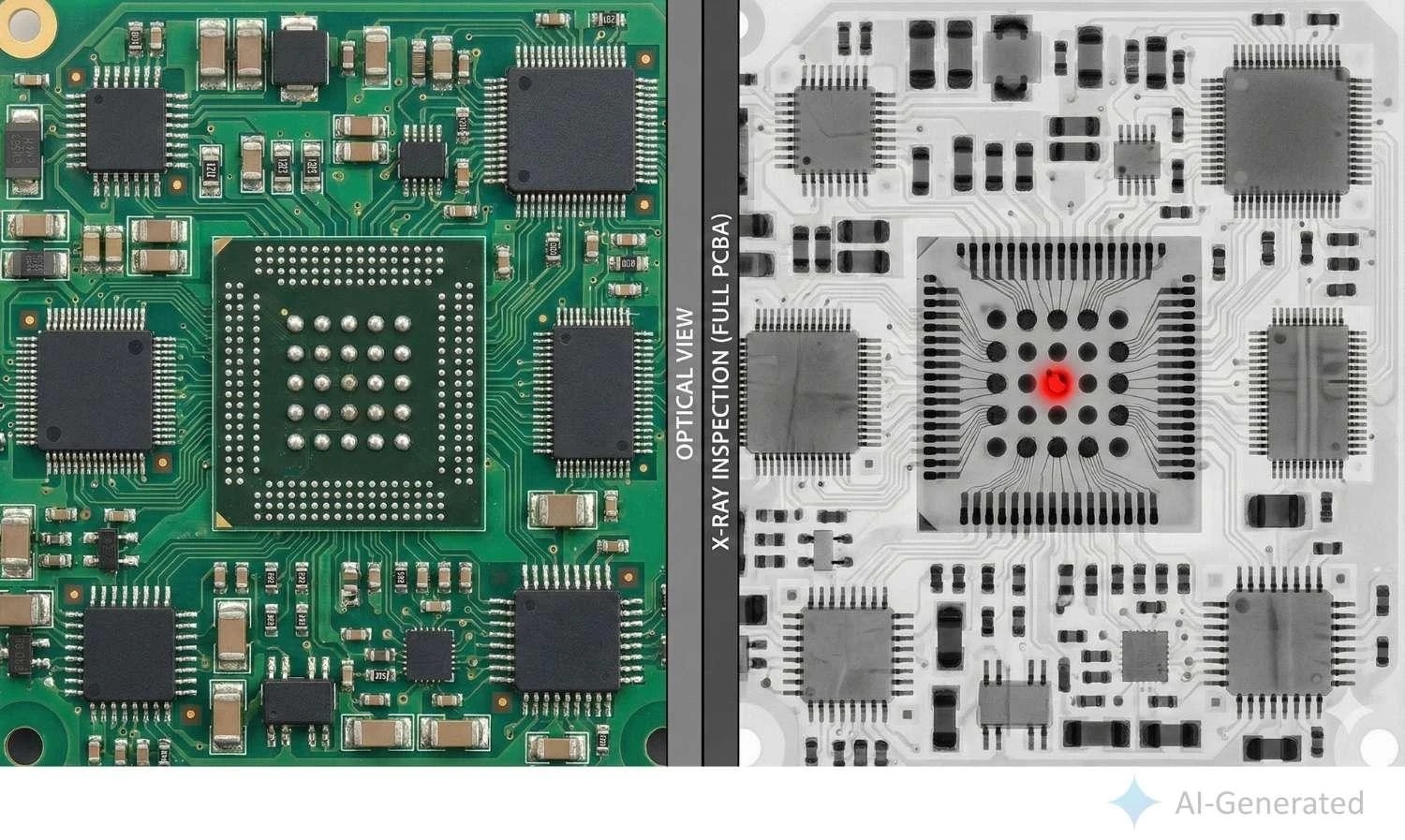
PCB X-ray inspection, also known as Automated X-ray Inspection (AXI), is a non-destructive testing (NDT) technique used in PCB assembly to evaluate internal features that are not visible to optical inspection.
AXI uses X-rays to penetrate PCB materials and electronic components, generating transmission images that reveal internal structures such as hidden solder joints beneath BGA, QFN, or LGA packages, solder fill quality in through-hole barrels, and internal wire bonds. Unlike Automated Optical Inspection (AOI), which inspects only visible surface features using reflected light, X-ray inspection enables the detection of subsurface defects, including voids, insufficient solder, bridging, and misalignment. As a result, PCB X-ray inspection plays a critical role in ensuring solder joint reliability, especially for high-density, fine-pitch, and advanced packaging technologies.
Why X-Ray Inspection Is Essential for Modern PCBs
As density increases, "line of sight" disappears. Implementing PCB X-Ray Inspection improves manufacturing quality through several key advantages:
Pros
- Hidden Joints: BGAs, CSPs, and Flip Chips have solder joints entirely underneath the package, making them invisible to optical inspection.
- High Density: 01005 passives and high-density interconnects (HDI) require precision that manual inspection cannot provide.
- Reliability: For JLCPCB's industrial and automotive clients, verifying void percentages is critical to preventing thermal failure.
- Early Defect Detection and Yield Improvement: Identifying internal defects like voids or bridges before functional testing prevents expensive scrap and rework. Catching issues early significantly boosts First Pass Yield (FPY).
- Feedback Loop for Process Optimization: X-ray data provides quantitative feedback to the SMT line. If void rates rise, engineers can immediately adjust reflow profiles or stencil apertures, preventing defect outbreaks.
How PCB X-Ray Inspection Works
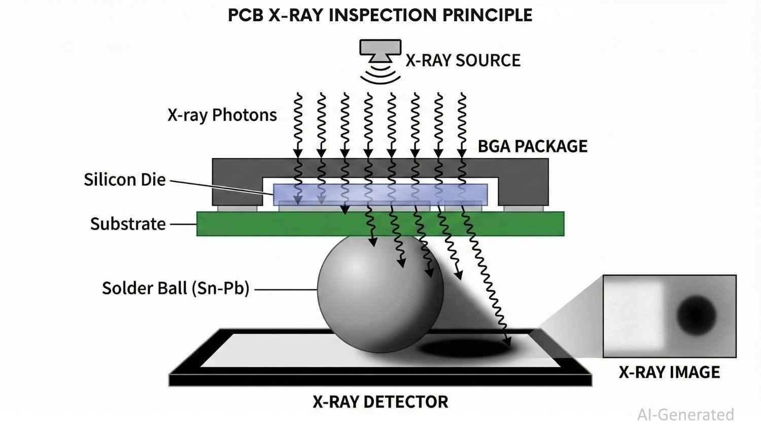
Basic Principle of X-Ray Imaging
X-ray PCB inspection functions based on the differential absorption of X-rays. When photons (30-160 keV) penetrate a PCBA, materials absorb them based on atomic number (Z) and density.
- High Attenuation (Bright White): Lead-free solder alloys (SAC305: Tin-Silver-Copper) with atomic numbers of 50 (Sn), 47 (Ag), and 29 (Cu).
- Moderate Attenuation (Grey): Copper traces (Z = 29).
- Low Attenuation (Dark): The X-ray absorption of the FR-4 substrate material and silicon die (Z = 14) is so low that they are seen as the darkest parts of the image.
This attenuation differential creates gray-scale images where solder joints, component leads, and internal structures become visible. The image contrast follows the Beer-Lambert law:
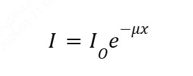
Where I is the transmitted intensity, I0 is the incident intensity, μ is the linear attenuation coefficient, and x is the material thickness.
2D X-Ray vs 3D CT X-Ray Inspection
| 2D X-Ray | 3D X-Ray / CT | |
|---|---|---|
| Methodology | Single-angle projection (Shadow map) | Multiple projections + volumetric reconstruction |
| Resolution | 3-5 μm | 0.5-2 μm |
| Inspection Speed | 60-200 boards/hour | 5-20 boards/hour |
| Void Detection Accuracy | ±3-5% | ±1-2% |
| Layer Differentiation | Limited (Overlapping features) | Excellent (Isolated slices) |
| Cost Range | $80K - $250K | $350K - $800K+ |
| Best Application | High-volume inline inspection | Failure Analysis, R&D, Complex PCBA |
PCB Components That Require X-Ray Inspection
BGA X-Ray Inspection
Ball Grid Arrays are the primary driver for X-ray adoption. Inspection verifies:
- Ball Shape: Ensuring reflow collapse is uniform.
- Alignment: Checking for offset between the BGA ball and PCB pad.
- Voiding: Quantifying gas pockets within the solder sphere.
QFN / LGA X-Ray Inspection
For Leadless packages, the critical focus is the Thermal Pad.
- Grounding: Ensuring the large central pad is soldered to the PCB ground plane.
- Fillet Inspection: Verifying wetting on the sidewall terminations, though X-ray primarily measures the solder volume underneath.
Through-Hole and Multilayer PCBs
X-ray penetrates the board substrate to inspect Plated Through-Hole (PTH) integrity.
- Barrel Fill: Confirming solder has filled >75% of the barrel vertical height (per IPC Class 2).
- Layer Alignment: In multilayer boards (up to 32 layers at JLCPCB), X-ray ensures drill holes align perfectly with internal copper rings.
Common Defects Detected by PCB X-Ray Inspection
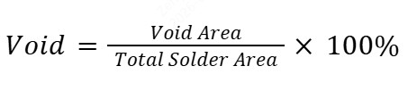
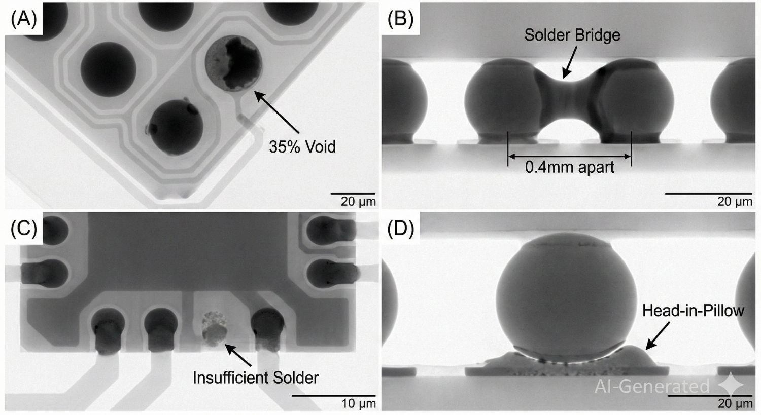
1Solder Voids and Void Percentage
Voids are air pockets trapped during reflow. Ball Grid Array inspection is the primary driver for X-ray adoption. Modern BGAs with 0.4mm pitch create solder joints completely hidden from optical view.
- Risk: High voiding reduces thermal conductivity and mechanical strength.
- Measurement: Void percentage is calculated as the ratio of void area to total ball area in the X-ray image.
2Open Joints and Head-in-Pillow (HiP)
Open Joints (Non-Wetting): An open joint occurs when there is a complete physical separation between the component termination and the PCB pad. On an X-ray, this typically appears as a perfectly spherical solder ball (indicating it did not wet and collapse onto the pad) or significantly smaller in diameter than adjacent functional joints.
Head-in-Pillow (HiP): A notorious and subtle defect where the BGA ball rests on the solder paste but fails to coalesce, often due to component warpage or oxidation. Unlike a complete open, HiP creates an intermittent electrical connection. X-ray detects this by identifying a distinct "waist" shape or separation line in the solder profile, which is invisible to optical inspection.
3Solder Bridging and Shorts
Bridges appear as bright white bands connecting adjacent pads. X-ray is the only way to detect bridges under BGAs or shielding cans.
4Insufficient or Excessive Solder
By analyzing grayscale density (thickness), algorithms determine if a joint is "starved" (insufficient solder volume) or bloated (excessive), which could lead to shorts.
5QFN Thermal Pad Voiding
Quad Flat No-lead packages concentrate connections on a central ground pad. Excessive voids (>20-30%) compromise thermal dissipation. X-ray imaging measures the actual solder volume and wetting angles along the component edge.
PCB X-Ray Inspection vs Other Inspection Methods
-
Technology
Uses X-ray photons to penetrate materials and generate internal images
-
Best For
BGA, QFN, LGA, CSP, and hidden solder joints
-
Limitations
Cannot detect electrical faults; slower than AOI; higher equipment cost
-
Technology
Uses cameras and reflected light for surface-level inspection
-
Best For
Component presence, polarity, visible solder fillets (0201s, SOIC)
-
Limitations
Cannot see under packages (BGAs, QFNs); no subsurface defect detection
-
Method
Physical structure verification using X-ray imaging
-
Detection
Finds "marginal" joints (HiP, excessive voiding) that may pass electrical testing but fail mechanically later
-
Method
Electrical probe testing for resistance, capacitance, and logic
-
Detection
Finds "dead" parts or hard shorts; may miss mechanical weaknesses
Note
When X-Ray Inspection Is Necessary: BGAs, LGAs, CSPs, QFNs with thermal pads, Metal Can Shields.
When It Is Not: Simple SMT (resistors/caps) and SOIC packages where optical inspection (AOI) provides sufficient coverage faster and cheaper.
IPC Standards and Acceptance Criteria for X-Ray Inspection
Relevant IPC Standards
- IPC-A-610: "Acceptability of Electronic Assemblies."
- IPC-7095: "Design and Assembly Process Implementation for BGAs."
Void Acceptance Guidelines for BGA and QFN (IPC Class 2)
| IPC Class 2 (Standard) | IPC Class 3 (High Reliability) | |
|---|---|---|
| BGA Ball Void % (Individual) | <25% | <15% |
| BGA Ball Void % (Cumulative) | <30% | <20% |
| Thermal Pad Void % | <30% | <20% |
| Solder Bridges | Not Acceptable | Not Acceptable |
| Insufficient Solder (Coverage) | >75% termination coverage | >90% termination coverage |
| Component Misalignment | <50% of electrode width | <25% of electrode width |
The quality control standards of JLCPCB follow the IPC Class 2 criteria with strict adherence in all assembly classes. Thus, through robotics and consumer applications, we guarantee the quality of their products or services.

Limitations of PCB X-Ray Inspection
What X-Ray Cannot Detect
- Electrical Logic: It cannot tell if a chip is fried internally or blank, only if it is soldered correctly.
- Zero-Contrast Materials: Aluminum wire bonds on aluminum pads (common in some COB tech) are hard to image without an advanced phase-contrast X-ray.
- Cold Solder Joints (Sometimes): If the solder shape is perfect but the metallurgical bond is weak, X-ray might miss it (unlike physical pull testing).
Cost and Throughput Considerations
- Bottleneck: X-ray is significantly slower than AOI. 100% X-ray inspection is often reserved for specific components (BGAs) rather than the entire board to maintain line throughput.
- Interpretation: While AI is improving, complex images (like CT reconstructions) often still require skilled operator review.
Technical Specifications and Selection Criteria for SMT X-Ray Inspection
Key Performance Parameters of SMT X-Ray Inspection Systems
Resolution: It is influenced by the size of the X-ray focal spot (1-10 μm) and the pitch of the detector pixels. The highest useful magnification is around 1000 times the size of the focal spot.
Tube Voltage: Selected based on sample thickness:
- 30-50 kV: Thin PCB assemblies (<1 mm) with low copper content.
- 60-90 kV: Standard SMT assemblies (1.6mm FR-4).
- 100-160 kV: Thick and multilayered (3-5mm), with a high copper percentage.
Detector Technology: Flat-panel detectors (Amorphous silicon or CMOS) have been preferred for their excellent image consistency and linearity over the older image intensifier technology.
Typical values shown below are indicative ranges. Actual performance depends on system architecture, focal spot size, detector resolution, and inspection mode (2D vs. CT).
| Resolution Required | Magnification Range | Tube Voltage | |
|---|---|---|---|
| BGA <0.4mm pitch | 2-3 μm | 500-1500X | 60-90 kV |
| Standard SMT (>0.5mm) | 5-8 μm | 100-800X | 50-80 kV |
| High-power modules | 5-10 μm | 50-500X | 80-130 kV |
| Aerospace/Medical (CT) | <1 μm | 1000-2000X | 90-160 kV |
Choosing a PCB Assembly Manufacturer with X-Ray Capability
When sourcing PCB assembly service, asking the right questions ensures your BGA designs are safe.
What to Ask Your PCB Assembly Supplier About X-Ray Inspection
-
Is X-Ray Inspection Inline or Offline?
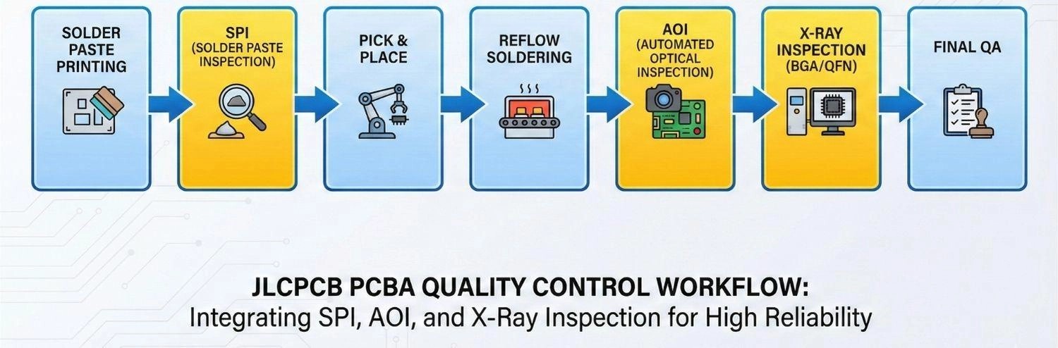
Inline allows for 100% inspection of critical parts in mass production without bottlenecks. Offline is typically used for sampling or detailed failure analysis (NPI). At JLCPCB, we integrate automated inspection directly into the quality control workflow, performing verification on BGA and QFN components as a standard inclusion.
-
What Type of X-Ray Technology Do You Use (2D vs. 3D/CT)?
For double-sided boards, basic 2D X-ray struggles with "shadowing" from components on the opposite side. 2.5D or 3D CT is essential for accurate defect detection in complex assemblies. JLCPCB's facilities utilize high-resolution systems capable of handling complex, double-sided layouts to ensure clear defect visualization.
-
What Are Your Reporting Capabilities?
A simple "pass" isn't enough for high-reliability projects. You need to verify if the supplier provides actual X-ray images, Void Percentage Heatmaps, or merely a text-based "Pass/Fail" log. Access to raw data is crucial for debugging reflow profiles. At JLCPCB, customers can request sample X-ray images and void analysis data, ensuring that the "Pass" status is backed by objective IPC-A-610 Class 2 data.
-
What Is Your Standard Sampling Strategy (100% vs. AQL)?
Some manufacturers only inspect 1 out of 50 boards (AQL sampling) to save time. For BGAs, 100% inspection is often preferred to catch random process anomalies. JLCPCB applies X-ray inspection for all BGA and QFN components to verify solder joint quality, ensuring no board leaves the line with hidden defects.
-
Are Your Operators Following IPC Standards?
Automated systems still flag "marginal" defects that require human judgment. Operators must be trained to distinguish between a harmless artifact and a true defect. JLCPCB's Quality Assurance team is trained on IPC-A-610 and IPC-7095 standards to make accurate, consistent accept/reject decisions.
Future Trends in X-Ray Inspection Technology
The new capabilities that are changing the PCB X-ray inspection world are:
- AI-Powered Defect Classification: Deep learning models that have been trained on millions of defect images can classify them with an accuracy that is more than 99%, thus cutting down the number of false calls and operator fatigue.
- Higher Resolution Micro-Focus: New types of tubes with <1 μm focal spots can give 5000-10000× magnification, which is very important for Fan-Out Wafer-Level Packaging (FOWLP).
- Real-Time 3D Imaging: Inverse geometry X-ray systems that have multiple detectors can get a CT dataset in seconds, thus making true inline 3D inspection possible for mass production.
FAQ about PCB X-Ray Inspection
Q: Does X-ray inspection damage sensitive semiconductor components?
In most cases, the answer is no. The modern X-ray inspection systems used for SMT take advantage of very low radiation levels, which are far below the limit that causes damage to silicon or trapping of charges in EEPROM/Flash memory, thus facilitating the inspection of active components with no risk.
Q: What is the IPC standard for allowable voiding in BGA X-ray inspection?
The IPC-A-610 Class 2 (the standard that JLCPCB adheres to) allows for individual voids of 25% of the ball area, which accounts for 30% cumulative voiding. Class 3 applications have a stricter standard (<15% individual voids). However, these applications usually require special manufacturing agreements to be set up.
Q: How does 3D X-ray (CT) differ from Laminography?
Both techniques provide depth information, but Computed Tomography (CT) usually does a complete rotation of the sample at 360 degrees for volumetric reconstruction. Laminography, on the other hand, does scanning by taking layers (slices) without performing the full rotation, which makes it faster and more suitable for flat PCBA panels in production environments.
Q: Can X-ray inspection detect microcracks in solder joints?
Microcracks (1-2 μm) can be detected by the high-resolution X-ray CT that reveals dark linear features within the bright solder volume. But for the extremely fine cracks (<1 μm) or delamination, complementary testing methods such as acoustic microscopy (C-SAM) or destructive cross-sectioning may be required.
Q: How does Automated X-Ray Inspection (AXI) differ from manual inspection?
The AXI systems are capable of processing 60-200 boards per hour using CAD-programmed coordinates along with AI-based defect recognition. Human-powered systems have to rely on the image positioning and interpretation done by the operators, resulting in a throughput of only 10-30 boards per hour. Although manual inspection is less costly for prototypes, AXI is unavoidable for mass production, even with a longer setup time.
Q: What X-ray tube voltage is optimal for thick multilayer PCBs?
The best range for standard 1.6mm FR-4 boards is 60-80 kV. For thick multilayer boards (3-5mm) with heavy copper, 90-130 kV is needed for good penetration. A common practice is to raise the voltage 10-15 kV for each extra millimeter of thickness to guarantee the desired contrast without penetration going too far.
Conclusion: Is PCB X-Ray Inspection Necessary for Your Project?
If your design includes BGAs, QFNs, LGAs, or ultra-fine pitch CSPs, PCB X-ray inspection is not optional — it is mandatory. Optical inspection simply cannot verify the reliability of these connections. By understanding the physics of attenuation and the IPC standards, you can better communicate your quality requirements.
From basic 2D void analysis to advanced 3D CT reconstruction, X-ray inspection provides the data needed to guarantee reliability. Whether you are building consumer electronics or industrial controllers, designing with testability in mind — and choosing a manufacturer like JLCPCB that prioritizes transparency — is the key to success.
Popular Articles
• PCB X-Ray Inspection Explained: Non-Destructive Testing for PCB Assembly Quality Control
• Flying Probe Testing: Revolutionizing PCB Quality Assurance in Modern Electronics Manufacturing
• Solder Paste Inspection (SPI): A Complete Guide to Process Control in SMT Assembly
• What Is PCBA Testing? Complete Guide to Inspection Methods, Process, and Quality Control
• Automated Optical Inspection (AOI): Principles, Defects, and PCB Applications
Keep Learning
PCB X-Ray Inspection Explained: Non-Destructive Testing for PCB Assembly Quality Control
In the era of miniaturization, modern printed circuit boards (PCBs) face an invisible challenge: verifying the quality of solder joints hidden beneath components. With Ball Grid Array (BGA) packages featuring pitch sizes down to 0.3mm and Quad Flat No-lead (QFN) components concealing critical thermal connections, traditional optical methods are blind to the most critical failure points. PCB X-ray inspection has emerged as the definitive solution. This guide explores the technical foundations, applicat......
Flying Probe Testing: Revolutionizing PCB Quality Assurance in Modern Electronics Manufacturing
The process for manufacturing printed circuit boards (PCBs) includes a critical testing phase. Each board must undergo testing to ensure manufacturers detect every electrical or circuitry problem before leaving the center. When a PCB passes this testing, it further ensures that it performs reliably. The most common types of testing methods include in-circuit testing (ICT) and flying probe testing (FPT). 6 high-precision probes (needles), 4 on top and 2 on the bottom are programmatically able to contac......
Transistor Pin Identification Using a Multimeter: Complete Step-by-Step Guide
Identifying transistor pins correctly is one of the first checks every engineer, hobbyist, and EE student needs before placing a bipolar junction transistor (BJT) into a circuit. A wrong base, collector, or emitter assignment can destroy the part on first power-up or leave a prototype board silently non-functional. This guide explains how to identify transistor pins using a multimeter when no datasheet is available. The method works because a BJT is internally built from two PN junctions sharing a com......
Solder Paste Inspection (SPI): A Complete Guide to Process Control in SMT Assembly
In today's Surface Mount Technology (SMT) manufacturing world, the consistency of the solder paste deposit is the element that drives electrical performance, mechanical shear strength, and long-term reliability of assembled Printed Circuit Boards. The solder paste is the medium that bonds the component terminations to the copper pads on the PCB. Therefore, any variations in the solder paste deposit in terms of volume, thickness, or placement will drastically impact the quality of the solder joints in ......
What Is PCBA Testing? Complete Guide to Inspection Methods, Process, and Quality Control
In modern electronics, the performance and long-term reliability of a finished product are directly tied to its Printed Circuit Board Assembly (PCBA) quality control. Even small defects at the board level—such as microscopic solder cracks, misaligned components, or incorrect passive values—can cascade into costly field failures, product recalls, and long-term damage to a brand's reputation. High-quality PCBA is not achieved through a single final inspection; it is the result of a repetitive and system......
Automated Optical Inspection (AOI): Principles, Defects, and PCB Applications
What Is Automated Optical Inspection (AOI)? Automated Optical Inspection (AOI) is a machine-based inspection method that uses high-resolution cameras, controlled lighting, and image-processing software to automatically detect visual defects on printed circuit boards (PCBs). It is widely used in PCB fabrication and PCB assembly to inspect components, solder joints, and conductor patterns without physical contact. By comparing captured images with design data or reference models, AOI systems can quickly......