
PCB Assembly for Wearable Devices: Tips, Materials, and More
9 min
- Key Design Challenges in Wearable PCB Assembly
- Flexible PCB Materials and Stack-Up Design for Wearable Devices
- Component Placement and Signal Routing in Wearable Flexible PCB Assembly
- SMT Assembly and Soldering Techniques for Wearable PCBs
- Protective Coating, Encapsulation, and Moisture Resistance in Wearable PCBs
- Power Management and RF Optimization in Wearable PCB Design
- Design for Manufacturability (DFM) Guidelines for Wearable PCB Assembly
- Common Failures and Prevention in Wearable PCB Assembly
- FAQ about Wearable PCB Assembly
- Conclusion: PCB Assembly for Wearable Devices
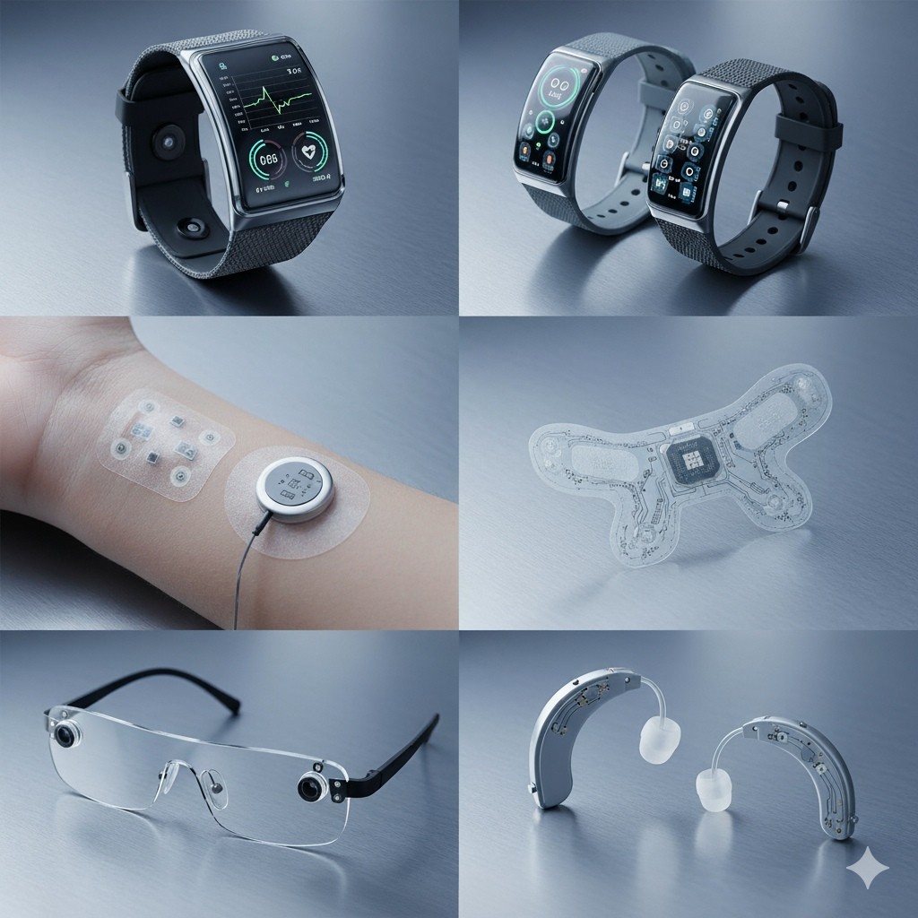
Wearable electronics — including health monitors, smartwatches, AR/VR headsets, and biosensors — represent one of the most transformative innovations in consumer and medical technology. These compact systems are engineered to deliver high functionality, user comfort, and long operational life simultaneously. This combination creates unique requirements for the printed circuit board assembly (PCBA) at its core.
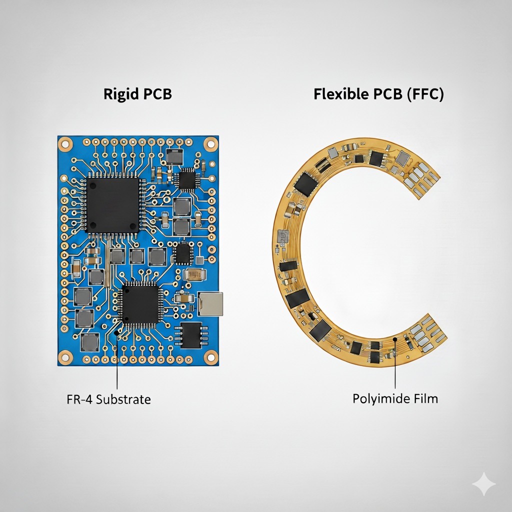
Unlike traditional rigid boards, PCBs used in wearables must be exceptionally thin, lightweight, and flexible. They are required to withstand continuous motion, body heat, and humidity.
To meet these demands, engineers employ flexible printed circuit boards (FPCBs), or flexible printed circuits (FPCs), which are fabricated using high-performance polyimide (PI) films. This material enables the circuits to bend and twist while maintaining electrical integrity and reliability.
JLCPCB specializes in manufacturing single- and double-layer flexible PCBs and providing high-precision PCB assembly service to meet the challenges of modern wearable devices.
This article outlines the engineering process for assembling PCBs for wearables — from material selection to reliability testing.
Key Design Challenges in Wearable PCB Assembly
Designing a PCB for a wearable device is a multifaceted engineering challenge. The competing constraints of space, power, and mechanical stress require specialized design solutions from the very beginning.
Wearable PCBs must combine mechanical adaptability with electrical reliability, making design optimization crucial from the start.
| Design Challenge | Description | Engineering Solution |
|---|---|---|
| Miniaturization | Limited area for ICs, sensors, and RF modules. | High-Density Interconnect (HDI) design, microvias, 0201 SMT components. |
| Flexibility | Must withstand continuous bending and twisting cycles. | Polyimide-based flexible PCBs (FPCs). |
| Power Efficiency | Small batteries severely limit runtime and thermal budget. | Low-power MCUs, optimized power planes, and efficient routing. |
| Moisture Resistance | Constant exposure to skin contact and sweat. | Conformal coating and encapsulation. |
| RF Stability | Antenna performance (detuning) is affected by the human body. | Controlled impedance routing and clear isolation zones. |
Also Read:
Flexible PCB Materials and Stack-Up Design for Wearable Devices
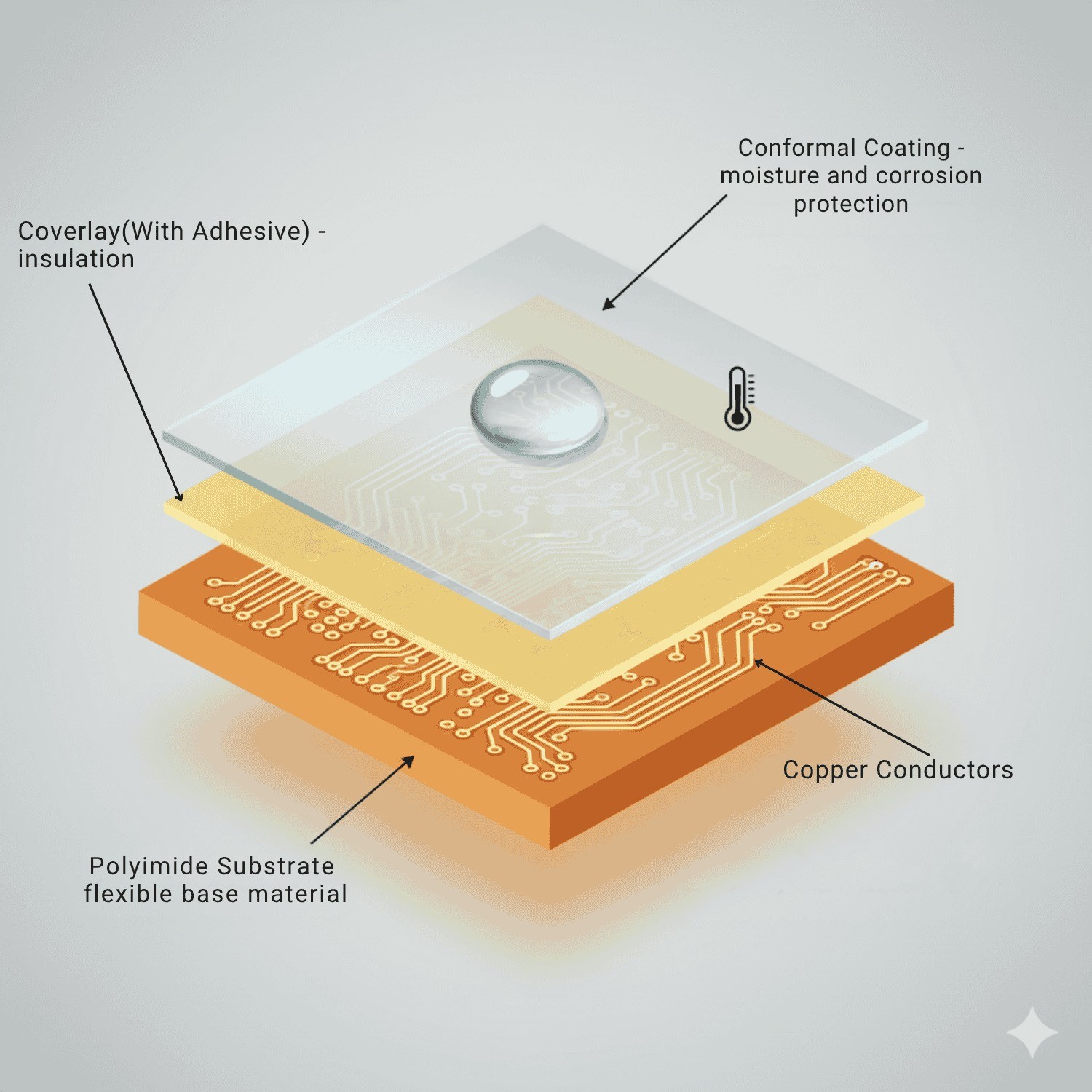
Although some complex wearable products still adopt a rigid-flex PCB approach, most applications are primarily designed around flexible PCBs, which are typically constructed from polyimide (PI) film, laminated with copper foil and a coverlay.
Key materials used in flexible PCBs for wearable devices include:
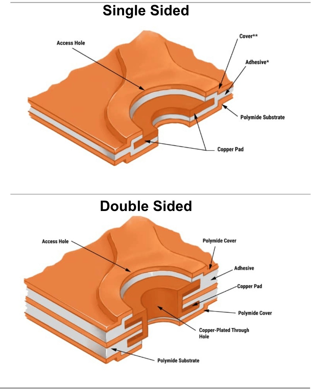
- Polyimide (PI): Serves as the base substrate. Polyimide is selected for its excellent flexibility, chemical resistance, and high thermal stability (withstanding temperatures above 260 °F / 130 °C).
- Copper Foil (12–70 µm): Acts as the conductive layer, providing stable electrical performance while minimizing resistive loss.
- Adhesive: A thermally rated bonding layer that secures the copper foil to the polyimide substrate.
- Coverlay: Usually made from polyimide, the coverlay provides insulation and mechanical protection, covering copper traces while defining openings for solder pads and vias.
JLCPCB supports single- and double-layer flexible PCBs based on high-performance polyimide films, offering outstanding reliability and excellent thermal endurance. These flexible, bendable, and foldable circuit designs are ideal for wearable electronics, IoT modules, and sensor applications.
Component Placement and Signal Routing in Wearable Flexible PCB Assembly
The layout of a flexible PCB for wearable devices directly impacts both electrical performance and mechanical reliability, particularly in applications that undergo repeated bending, twisting, or flexing.
Proper component placement and signal routing are critical to ensure that wearable electronics maintain functionality and durability over time.
Placement Guidelines for Wearable Flexible PCBs
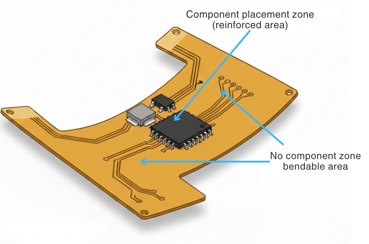
- Place larger or heavier components on sections of the PCB that remain mechanically stable during bending to reduce stress on solder joints.
- Avoid positioning ICs or connectors in active flex zones, as this can induce stress and compromise solder joint reliability.
- Keep routing on the neutral axis for routing in flex zones to minimize copper stress.
- Physically separate RF components (e.g., antennas) from digital circuitry to reduce interference, which is especially important in wearable devices with compact layouts.
Routing Guidelines for Wearable Flexible PCBs
- Use curved trace corners and teardrop-shaped pads to reduce stress concentration and prevent cracking in flex areas.
- Maintain a minimum bend radius of at least 10 times the total thickness of the FPC to ensure mechanical durability.
- Incorporate proper shielding and grounding techniques to minimize EMI and signal coupling, which is critical for sensors and wearable modules that rely on accurate signal transmission.
- Consider the placement of sensor interconnections carefully to avoid interference and maintain reliable data acquisition in multi-sensor wearable devices.
SMT Assembly and Soldering Techniques for Wearable PCBs
Assembling flexible PCBs for wearable devices requires careful thermal and mechanical handling to maintain both electrical integrity and mechanical reliability. Because thin polyimide (PI) films can warp during processing, FPCs for wearable electronics are typically mounted on rigid carrier pallets (jigs) throughout the entire SMT process, especially during reflow soldering.
To protect the flexible materials used in wearable PCBs, a low-temperature reflow soldering profile is commonly employed. This minimizes thermal stress on the polyimide substrate and adhesive layers, ensuring that delicate sensors, ICs, and other components remain fully functional in compact devices such as smartwatches, health monitors, and fitness trackers.
Proper handling and optimized reflow profiles are critical for reliable wearable PCB assembly, enabling flexible electronics to maintain durability under repeated bending and daily usage.
| Parameter | Range | Purpose |
|---|---|---|
| Ramp Rate | 1.0–1.5 °C/s | Prevents thermal shock and board distortion. |
| Soak Zone | 150–180 °C, 60–120 s | Activates flux and equalizes temperature across the assembly. |
| Peak Temperature | 220–230 °C | Suitable for low-temp solder (e.g., Sn42Bi58). |
| Time Above Liquidus | 50–70 s | Ensures proper solder wetting and joint formation. |
JLCPCB's SMT process includes:
- Automated pick-and-place assembly for components as small as 0201 packages.
- Nitrogen reflow soldering, which minimizes oxidation and improves solder joint quality.
- Automated Optical Inspection (AOI) and X-ray inspection for comprehensive quality control.
Protective Coating, Encapsulation, and Moisture Resistance in Wearable PCBs
Wearable devices are always exposed to sweat and environmental moisture. They need to be protected from moisture to avoid corrosion, oxidation, or potential short circuits.
A common protective method is Conformal Coating (Parylene, Acrylic, Silicone), which is a thin polymeric coating that allows moisture protection without reducing flexibility.
JLCPCB offers selective conformal coating and testing options to improve the long-term reliability of wearable devices.
Power Management and RF Optimization in Wearable PCB Design
Power efficiency and reliable wireless performance are critical design aspects for wearable IoT devices.
Power Optimization for IoT Wearables
- Use wide power traces and solid ground planes to minimize I²R losses.
- Use low dropout regulators (LDOs) and switching regulators for power-sensitive designs.
- Properly position decoupling capacitors as close to the component load as possible.
RF Design for IoT Wearables
- Maintain a clearance of 5–10 mm around the antenna from ground planes and components.
- Tune trace impedance (typically 50 Ohm) for the wireless module (e.g., BLE or Wi-Fi). Use JLCPCB's Controlled Impedance Calculator to tune trace impedance.
- Use ground shielding and vias to separate the RF section from noisy digital circuits.
Design for Manufacturability (DFM) Guidelines for Wearable PCB Assembly
During the PCB design stage of your wearable device, adhering to DFM guidelines is the most effective way to reduce/retrain rework, improve yields, and lower costs.
Best DFM Practices:
- The bend radius should be 10 times the total thickness of the FPC.
- Refrain from placing components, vias, etc., near the edges of the flex outline.
- Include fiducial markers to aid optical alignment in SMT equipment and, if needed, tooling holes.
JLCPCB provides a free DFM tool to check the design for manufacturability errors.
Common Failures and Prevention in Wearable PCB Assembly
Understanding potential failures in wearable PCBs is essential for designing robust wearable electronics.
| Issue | Cause | Solution |
|---|---|---|
| Solder Cracking | Excess bending stress on component joints. | Use underfill, place components off-bend-axis. |
| Delamination | High reflow temperature or moisture in FPC. | Pre-bake FPCs; use low-temp solder and proper adhesion. |
| Corrosion | Moisture ingress from sweat or humidity. | Apply conformal coating and ensure a complete seal. |
| RF Drift | Antenna proximity to the human body or ground. | Maintain ground clearance; tune antenna in situ. |
FAQ about Wearable PCB Assembly
Q: Can flexible PCBs have both signal and power layers?
Yes. Multi-layer flexible PCBs can incorporate both signal and power traces. However, designers must carefully control impedance and maintain copper balance to ensure consistent mechanical reliability and bending performance.
Q: What surface finish options are recommended for wearable PCBs?
ENIG (Electroless Nickel Immersion Gold) and OSP (Organic Solderability Preservative) are the most commonly used surface finishes for wearable applications. Both finishes provide excellent corrosion resistance and long-term solderability, which are essential for maintaining reliability over time.
Q: Can sensors be integrated into flexible PCBs?
Yes. Many modern flexible PCBs integrate temperature, pressure, or biosensing components directly into the flexible substrate to reduce footprint and enhance signal accuracy. This integration supports compact, multifunctional wearable designs.
Q: How do trace width and spacing affect PCB flexibility in wearables?
Using narrower traces (≤0.1 mm) and wider spacing improves the overall bending capability of the PCB. Avoid sharp trace angles and uneven copper distribution, as these can cause stress concentration and lead to mechanical failure during flexing.
Conclusion: PCB Assembly for Wearable Devices
Wearable electronics continue to transform modern engineering by driving advancements in flexibility, performance, and compactness. Flexible printed circuit boards (FPCs) enable lightweight, durable, and adaptable designs that power next-generation medical, fitness, and IoT devices.
Achieving high-quality assembly and strict adherence to specifications through SMT assembly and rigorous testing is essential to ensuring the reliability of wearable devices operating in dynamic environments.
JLCPCB provides the stable foundation engineers need to design wearable products that are both reliable and production-ready — applying advanced process control and meticulous attention to every aspect of design and manufacturing.

Keep Learning
PCB Assembly for Wearable Devices: Tips, Materials, and More
Wearable electronics — including health monitors, smartwatches, AR/VR headsets, and biosensors — represent one of the most transformative innovations in consumer and medical technology. These compact systems are engineered to deliver high functionality, user comfort, and long operational life simultaneously. This combination creates unique requirements for the printed circuit board assembly (PCBA) at its core. Unlike traditional rigid boards, PCBs used in wearables must be exceptionally thin, lightwei......
Integrating Raspberry Pi with PCB Design for Cutting-Edge Projects
Introduction The Raspberry Pi has revolutionized the world of electronics with its affordability and versatility. When combined with PCB (Printed Circuit Board) design, it offers a range of exciting possibilities for hobbyists and engineers alike. This article dives into how Raspberry Pi in PCB design is transforming the landscape of electronics. From integrating Raspberry Pi into custom PCBs to exploring advanced projects, we’ll guide you through practical tips and insights on Raspberry Pi Integratio......
Arduinos and PCBs Comprehensive Integration Guide
Introduction In the realm of electronics, the Arduino PCB is a vital component for enthusiasts and professionals alike. The Arduino microcontroller platform has revolutionized PCB design for Arduino, allowing for unique and customizable Arduino circuit designs. By integrating Arduino with PCBs, you open up a world of possibilities for creating specialized electronic devices. This article delves into the integration of Arduinos with PCBs, focusing on Arduino circuit design, the creation of custom Ardui......
Discover the Power of ESP32 Microcontroller Projects
The ESP32 microcontroller is a favorite among tech enthusiasts for its amazing features and versatility. It boasts a dual-core processor, Wi-Fi, and Bluetooth, making it ideal for various DIY and professional projects. In this article, we'll look at some exciting ESP32 projects, from home automation to environmental monitoring that will show you how to make the most of this microcontroller. Home Automation with ESP32 Home automation is one of the most popular uses for the ESP32. Its built-in Wi-Fi and......
3D Printed PCB Explained: Technology, Materials, Pros, Cons, and Applications
3D printed PCBs are redefining how electronic circuits can be designed, prototyped, and integrated into complex structures. Unlike traditional FR-4 boards, this additive manufacturing approach enables conformal geometries, structural electronics, and rapid iteration without tooling or chemical etching. This article explains what 3D printed PCBs are, how they work, their key advantages and limitations, and how they compare to conventional PCBs—helping engineers and product designers understand when thi......
Comprehensive Guide to the ESP32 Microcontroller Powering IoT Innovations
Introduction The ESP32 microcontroller has rapidly become a cornerstone in the world of IoT (Internet of Things), providing developers and hobbyists with a versatile, powerful, and cost-effective platform. This article delves into the definition of ESP32, its usage in various applications, and provides examples to highlight its capabilities. With its robust feature set, the ESP32 is not just another microcontroller but a game-changer in the IoT landscape. ESP32 Definition: The ESP32 is a low-cost, low......