Step Stencil Design: The Complete Technical Guide
25 min
- What Is a Step Stencil?
- When Your Board Actually Needs an SMT Step Stencil?
- Step Stencil Design Principles That Determine Yield
- How Step Stencil Manufacturing Shapes Design Decisions?
- Step Stencil Materials, Thickness Profiles, and Surface Treatments
- Common Step Stencil Defects and How to Prevent Them
- FAQs About Step Stencil Design and Manufacturing
- Conclusion: Get Your Step Stencil Design Right the First Time
Key Takeaways
- A multi-level stencil places different foil thicknesses in distinct zones—thinner for fine-pitch components, thicker where high-mass joints need more paste volume.
- Typical step depths run 0.025 mm to 0.05 mm (25–50% of base foil thickness). Exceeding 50% risks mechanical failure, foil fatigue, and print inconsistency.
- Maintain 1.5–2.0 mm clearance between any aperture and the nearest step edge to prevent squeegee bounce, paste scooping, and volume variation.
- Modern step stencil manufacturing combines laser cutting with chemical step etching. Pure chemical etching alone is no longer appropriate for fine-pitch SMT work.
- Electropolishing matters more on stepped foils than flat ones. Step transitions need ultra-smooth walls for reliable squeegee travel and clean paste shear.
- A step stencil costs more upfront than a flat stencil, but far less than two separate print passes with all the added cycle time, equipment overhead, and cleaning requirements.
- Always verify that apertures inside step-down zones maintain an area ratio of ≥ 0.66 per IPC-7525B. In fact, thinning the foil in a step-down zone raises the area ratio — which is exactly why fine-pitch apertures belong in the thinner zone for cleaner paste release.
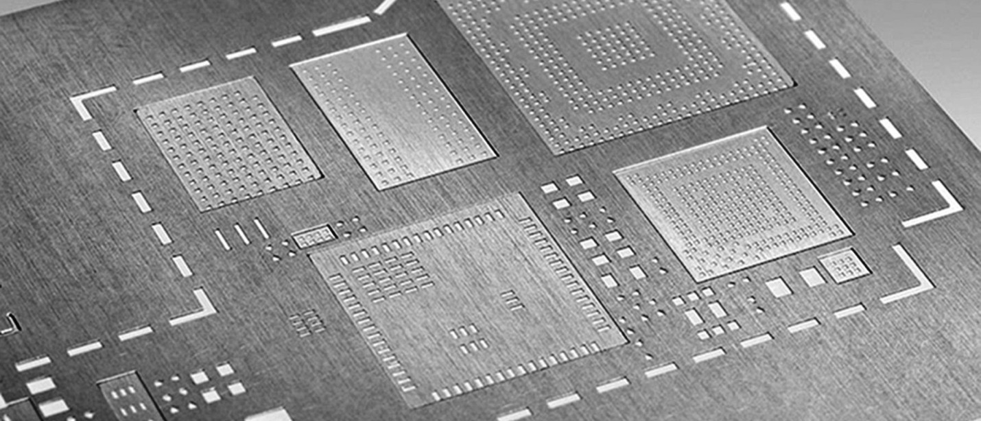
Real-world PCB layouts rarely play nice. A board carrying fine-pitch BGAs right next to large RF shields or a mix of 0201 discrete chips and QFN thermal pads creates a paste-volume conflict that a single-thickness flat stencil simply cannot solve.
A proper step stencil design resolves this by introducing deliberate thickness variations, typically 0.025 mm to 0.05 mm steps, to deposit exactly the right paste volume in each zone.
In this guide, we reveal the design parameters that determine print yield, manufacturing methods, and their real tradeoffs. Along with that, we discuss material and surface treatment selection, and the defect modes that surface when any of these elements fall short.
What Is a Step Stencil?
A Working Definition for Engineers
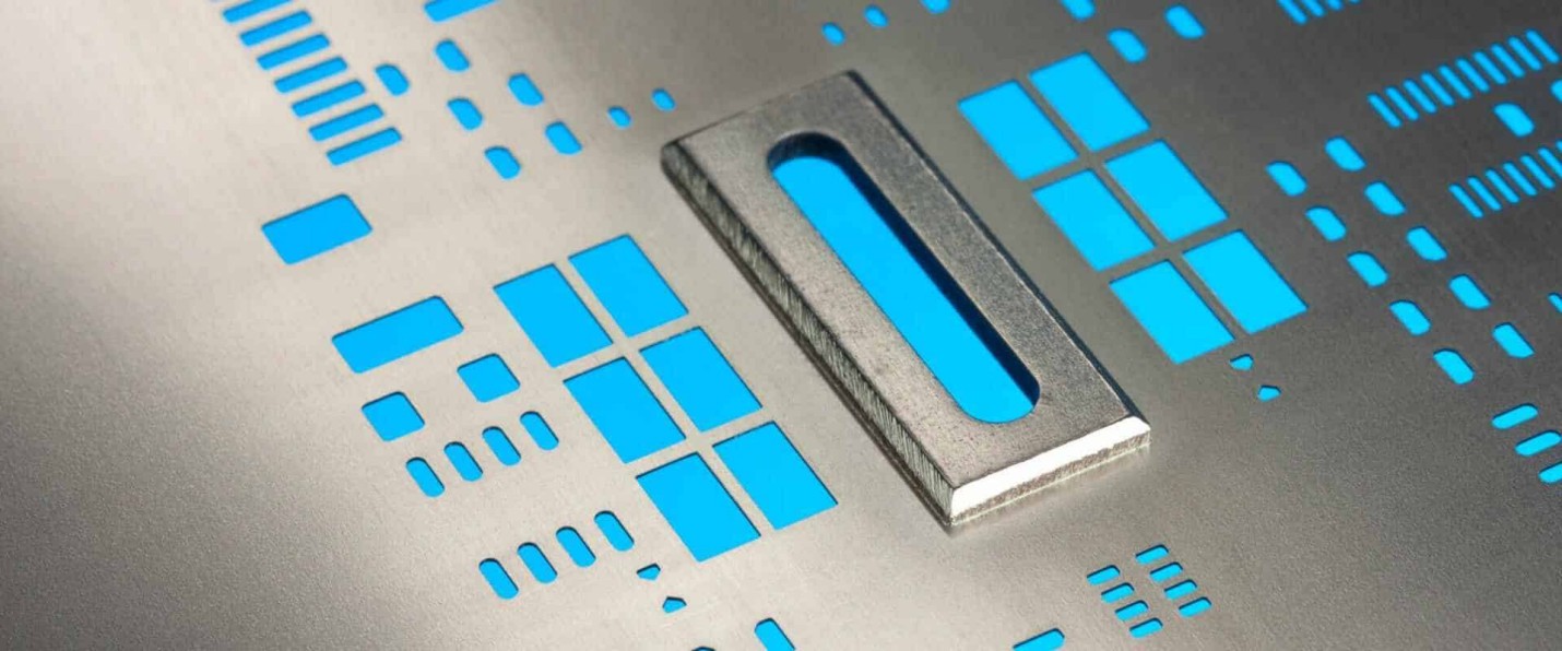
A step stencil, also called a multi-level stencil or stepped stencil in some regional usage, is a single SMT foil that carries two or more deliberately different thicknesses, joined by precision step transitions.
Each thickness zone is engineered to control the paste deposit height in that area, matching the volumetric requirement of the components placed above it. The goal is a single print pass that satisfies every component class on the board simultaneously, without compromise.
Step-Up vs. Step-Down: A Quick Recap
Step stencils come in two fundamental configurations. A step-down stencil design etches a recessed, thinner zone into a thicker base foil—the right choice when most of the board needs standard paste volume, but isolated fine-pitch areas like 0.4 mm BGAs or dense QFN pads need a reduced deposit to prevent bridging.
A step-up stencil design does the opposite: a thicker region is built over a thinner base. Apply it when most components are fine pitch, but a few high-mass parts (such as power connectors or RF shield walls) require a larger paste volume to form solid, reliable joints.
See the Beginner's Guide to Step-Up and Step-Down Stencils to learn more.
When Your Board Actually Needs an SMT Step Stencil?
Boards That Clearly Benefit
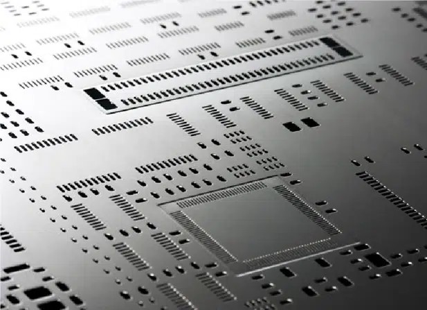
Not every mixed-component assembly needs a stepped foil. But certain board classes make the case obvious from the start.
-
Mixed-pitch layouts are the most common trigger, combining fine-pitch BGAs or QFNs (0.4 mm pitch and below) with standard- or large-pitch connectors on the same board. A flat stencil optimized for one group will inevitably starve or flood the other. There is no middle ground that works reliably at volume.
-
Paste-in-hole (PiH) assemblies put the conflict in sharp relief. Through-hole barrels require significant paste volume to fill vertically and form sound joints; the SMT passives sitting a few millimeters away need a thin, tightly controlled deposit. No single flat stencil thickness satisfies both.
-
RF shielding cans demand continuous, high-volume paste deposits along their perimeter to ensure mechanical adhesion and reliable EMI performance. Fine-pitch logic in the vicinity makes a flat stencil an inevitable compromise.
-
High-current power components alongside fine-pitch signal devices present the same core problem. Large thermal pads and power MOSFETs need paste volumes that would cause bridging on adjacent 0.4 mm pitch ICs.
Boards Where a Flat Stencil Is Sufficient
Stepped foils add cost and design verification effort. A standard flat stencil is the right call when components share similar paste volume requirements: pure fine-pitch layouts, advanced logic boards with only micro-BGAs and small discrete passives, standard-pitch consumer electronics where all passives are 0805 or larger, and pitch stays comfortably above 0.65 mm, or cost-sensitive prototypes where minor volume variation is acceptable, and aperture modifications on a flat foil can compensate adequately.
Alternatives Worth Evaluating First
Before specifying a stepped foil, a few simpler approaches deserve a look. Aperture reduction on a flat stencil trims opening dimensions by 5–20% to reduce paste volume on overfilled pads. This works when the area ratio stays safely above 0.66, and the volume mismatch is not severe.
Two stencils, two print passes are technically clean, but double cycle time, equipment occupancy, and cleaning requirements; the economics rarely favor this approach beyond low-volume prototyping.
Jet dispensing for outlier components adds paste to specific pads after a standard print run—accurate, but a throughput bottleneck in any production environment running at high volume.
| Method | Tooling Complexity | Cycle Time | Volume Range | Yield Risk | Best Application |
|---|---|---|---|---|---|
| Flat Stencil (Aperture Reduction) | Low | Fast (single pass) | Low variation | Medium | Moderate pitch variation |
| SMT Step Stencil | Medium | Fast (single pass) | High | Low | Mixed-pitch, RF shields, PiH |
| Two-Pass Printing | High | Slow (double pass + clean) | Extreme | Low | Extreme component mismatch |
| Jet Dispensing | High | Slow (sequential) | Extreme | Low | Low-volume, high-mix |
Step Stencil Design Principles That Determine Yield
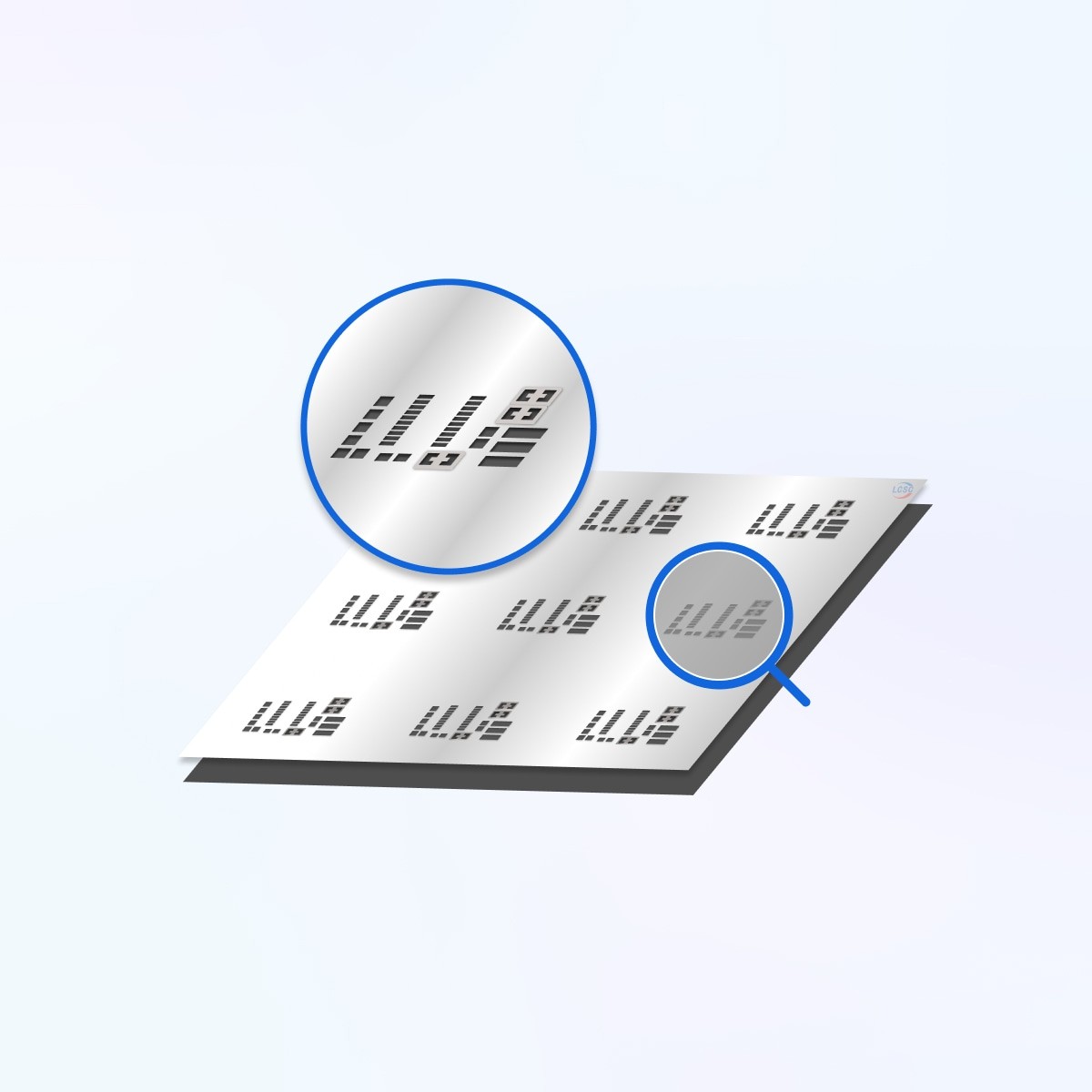
This is where most design errors originate. The physical constraints of stepped foils impose rules that simply do not apply to flat stencils, and overlooking them is the fastest route to production defects.
Step Depth: How Much Thickness Variation Is Safe
The height difference (ΔT) between the base foil and the stepped zone typically falls between 0.025 mm and 0.05 mm (1–2 mils). Per IPC-7525B, the upper limit for safe step depth is:
ΔT ≤ 0.50 × T_base
Exceeding 50% of base foil thickness introduces mechanical stress concentration at the step boundary. To understand why, consider that the step transition creates an abrupt change in cross-sectional area across the foil. Under the cyclic compressive and tensile loads applied by the squeegee, that geometric discontinuity behaves like a notch in a loaded beam, a classic stress riser. Each print stroke deposits a small increment of plastic strain at the notch root. Over thousands of cycles, this accumulates into micro-cracking and foil fatigue, visually indistinguishable from normal wear until the stencil begins producing erratic joint heights. The lower practical bound sits around 0.025 mm; anything shallower produces negligible paste volume change and is not worth the added tooling cost.
Step Stencil Aperture Clearance and Buffer Zones
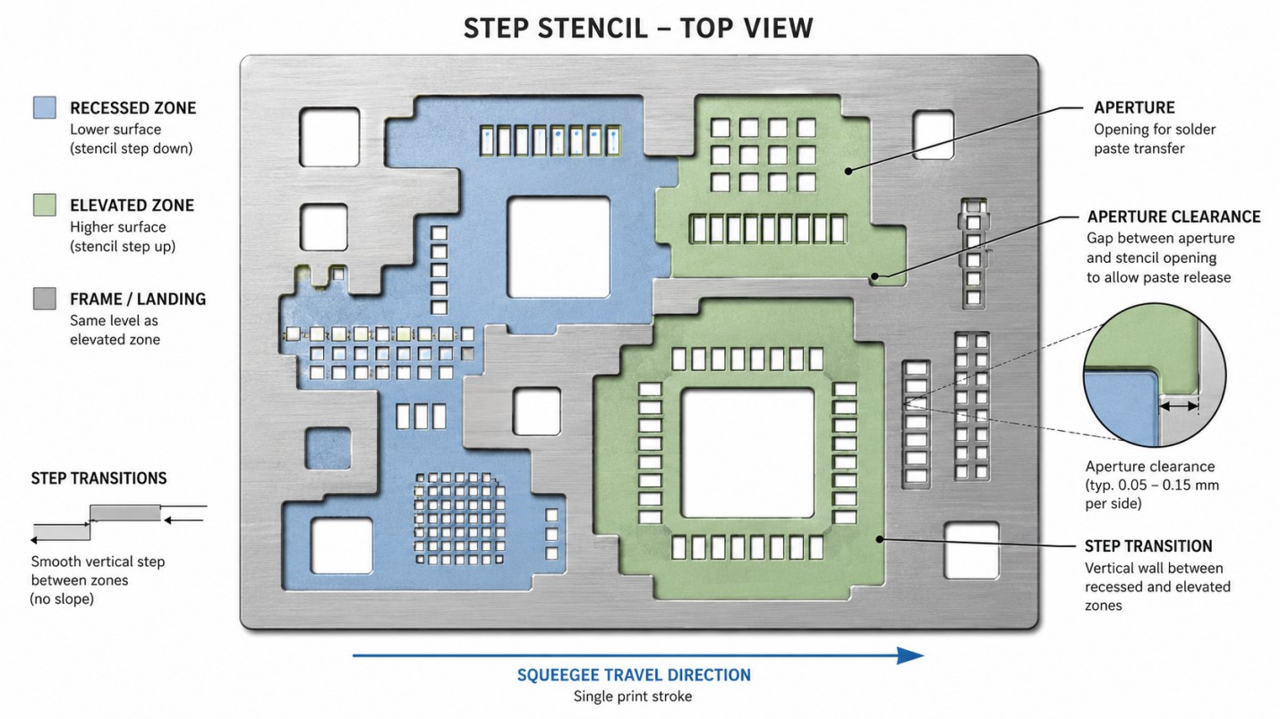
Placing apertures too close to step edges is one of the most common mistakes in step stencil design. To understand why, consider what happens physically as the metal squeegee blade crosses a step boundary at speed. On the approach to a step-up, the blade encounters a rising surface: the leading edge momentarily deflects upward, reducing contact pressure on the foil immediately behind it. Any aperture sitting in that pressure-recovery shadow receives an incomplete fill — the paste column is shorter because the blade did not maintain full downward force during the transit. On a step-down, the reverse occurs: the blade briefly "falls" into the recessed zone, and the sudden pressure spike at the step edge can scoop paste from apertures near the boundary, producing overprinted deposits on one side and underprinted ones on the other.
IPC-7525B identifies a minimum keep-out distance from step edges. The industry-standard practical rule is:
K₁ ≥ 1.5–2.0 mm from any step boundary to the nearest active aperture
A minimum of 0.65 mm can function for apertures located in the thicker (elevated) zone on standard print setups, but 1.5 mm should be treated as the floor for any aperture in a thinned zone or immediately adjacent to a boundary crossing.
Worked example: A 0.15 mm base foil stepped down to 0.10 mm has ΔT = 0.05 mm. Some suppliers quote a 10× rule (10 × ΔT = 0.5 mm minimum clearance), but the IPC floor of 1.5 mm governs. Any fine-pitch apertures placed tighter than 1.5 mm from that step boundary will exhibit statistically significant deposit variation in SPI data.
Step Zone Shape and Layout
Step zone geometry directly affects squeegee pressure uniformity throughout the print stroke. Rectangular zones aligned parallel or perpendicular to squeegee travel are the most forgiving: the blade hits the step edge at a uniform angle across its full width and maintains consistent pressure as it crosses. Think of it as the difference between walking straight off a curb versus hitting it at a diagonal. The asymmetric impact creates an uneven pressure wave that takes longer to stabilize.
Diagonal or curved step boundaries force the blade to engage the transition at a continuously varying angle, creating a pressure gradient across adjacent apertures that shifts paste fill from one end of the blade to the other in real time. If a non-rectangular step zone is geometrically unavoidable, specifying a micro-machined ramp transition, a shallow-angled slope rather than a vertical wall, reduces the pressure discontinuity and gives the blade more gradual engagement with the height change. Electropolishing the transition wall further reduces the tendency to catch. Keep step zones away from board edges; the squeegee needs a flat run-in and run-out distance to stabilize pressure before any step transition begins.
Area Ratio in Step-Down Zones
This constraint is unique to stepped foils and is frequently overlooked until paste trials expose the problem. The area ratio (AR) is the ratio of aperture opening area to its interior wall area. It governs the balance between the force pulling paste out of the aperture (squeegee pressure and gravity) and the force holding it in (wall friction and surface tension). When the AR falls below the IPC-7525B minimum of 0.66, the surface tension and wall-friction forces win: paste remains trapped inside the aperture instead of releasing cleanly onto the pad, producing a starved or misshapen joint.
Here is the point most engineers get backwards: thinning the foil in a step-down zone does not compress the area ratio — it increases it. Because foil thickness sits in the denominator of the AR formula, reducing T from T_base to T_step shrinks the aperture wall area and pushes the ratio up. An aperture sitting right at AR 0.66 on a 0.15 mm base climbs to roughly AR 0.99 once the local thickness drops to 0.10 mm, with no change in aperture dimensions at all. This is precisely why fine-pitch components are placed in the thinner step-down zone: the reduced thickness simultaneously cuts paste volume (preventing bridging) and lifts the area ratio (improving release).
AR = (L × W) / (2 × (L + W) × T_step) ≥ 0.66
Where L = aperture length, W = aperture width, and T_step = local stepped-down foil thickness. Still recheck every aperture in the zone once the step depth is finalized — a small fine-pitch aperture can sit below 0.66 even in a thinned zone simply because L and W are tiny. If any fall short, the levers are to widen the aperture (increase L or W), thin the zone further (a deeper step, within the 50% limit), apply electropolishing plus nano-coating to improve transfer efficiency, or switch to a rounded or home-plate aperture shape.
Squeegee Compatibility With Step Stencils
Polyurethane squeegee blades are fundamentally incompatible with stepped foils, and the physics explain exactly why. Polyurethane is a viscoelastic material: under dynamic load, it deforms rather than transmitting force rigidly. As the blade crosses a step-up boundary, rather than bridging the height transition and maintaining contact on both sides, it deforms to follow the profile, sagging into the recessed zone. This does two damaging things simultaneously: it scoops paste out of large apertures in the recessed area (overfill), and it loses contact pressure on the elevated zone (underfill). The blade is, in effect, acting as a paste redistributor rather than a paste printer, smearing volume from step-down zones to step-up zones in an uncontrolled way.
Metal squeegee blades are mandatory for stepped foils. The high modulus of spring steel means the blade bridges step transitions as a near-rigid beam: it contacts the high and low sides simultaneously, maintaining a controlled paste bead across both zones. The blade angle should be set between 45° and 60°, depending on the step height. Print speed typically needs to drop 10–20% compared to flat-stencil settings, roughly 20–30 mm/s for most step configurations, because slower traversal gives the paste bead more time to maintain hydraulic pressure into each aperture as it crosses the thickness transition.
How Step Stencil Manufacturing Shapes Design Decisions?
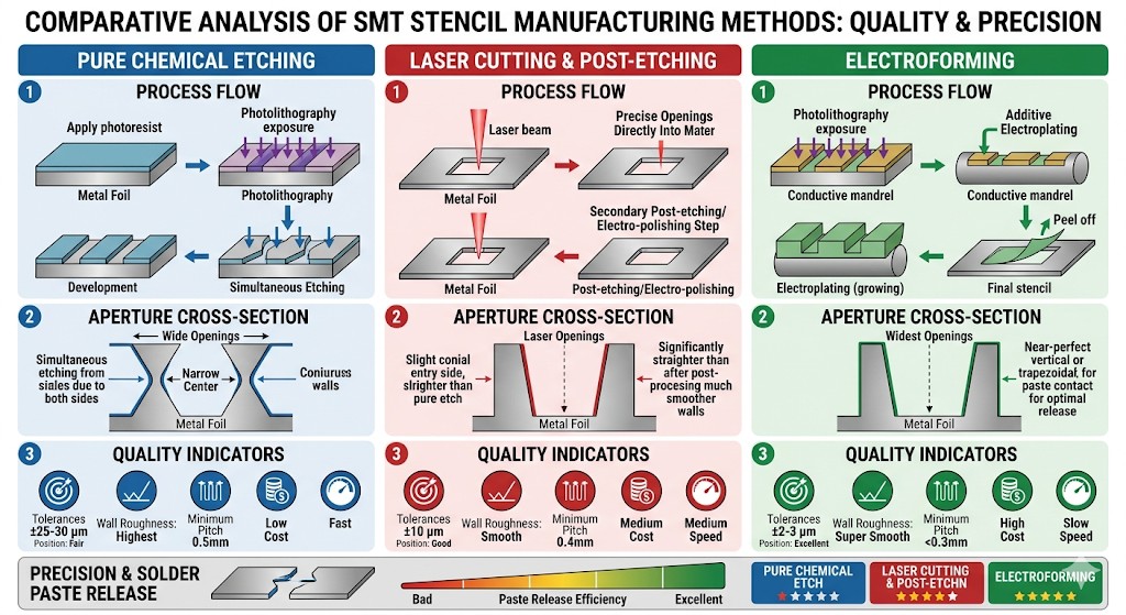
The fabrication process is not just a procurement detail. It sets real limits on achievable step geometries, tolerances, and aperture wall quality. Understanding these tradeoffs is part of sound step stencil design.
Laser Cutting Plus Step Etching
This two-stage hybrid process is the dominant method in modern production step stencil manufacturing. The process begins with selective wet chemical etching: a photoresist mask is laminated onto the stainless steel foil and exposed to define the step zone geometry. An acid bath then removes base material in the unmasked areas to the target step depth, after which the resist is stripped and the foil cleaned. Fiber laser cutting is used to form the aperture array across the entire foil with high positional accuracy.
The separation of these two operations is what gives the method its quality advantage. Chemical etching is well-suited to creating smooth, gradual step profiles across large area changes; laser cutting is well-suited to forming precise, sub-millimeter apertures with clean, consistent wall geometry. Neither process alone achieves what both achieve in sequence. The result is aperture tolerances down to ±0.003 mm and step depth control around ±5 µm. The fiber laser also imparts a slightly trapezoidal aperture wall; oriented with the wider opening on the bottom (PCB-contact side), this taper forms a positive draft angle that promotes clean paste release. Most production-grade step stencils are manufactured this way.
Electroforming
Electroforming is an additive manufacturing process that grows the stencil from the ground up rather than cutting material away. A conductive mandrel is machined or patterned to the inverse of the desired stencil geometry, then submerged in a nickel sulfamate electroplating bath. Nickel ions deposit onto the mandrel surface and build up layer by layer until the target foil thickness is reached. At the end of the process, the grown foil is separated from the mandrel, and the apertures are defined by the mandrel features rather than by post-process cutting.
The key consequence of this additive, atom-by-atom growth mechanism is that aperture walls are formed continuously and without any cutting or ablation. There are no laser slag deposits, no micro-burrs, and no heat-affected zones – the walls are simply smooth crystalline nickel with a surface roughness measured in nanometers rather than micrometers. This near-perfect wall finish means that paste release is dominated by bulk rheology and surface tension rather than by wall friction, allowing reliable transfer at area ratios approaching 0.50, well below what laser-cut stencils can consistently handle. The trade-off is real: electroforming requires a machined mandrel (significant upfront tooling costs), takes longer to produce, and yields pure nickel foil that is softer and more susceptible to damage than hardened stainless steel. High-cycle production lines with frequent stencil loading and unloading tend to damage electroformed stencils faster than laser-cut ones. Electroforming is best justified for high-volume automotive or medical assemblies where sub-0.3 mm pitch micro-BGAs make superior transfer efficiency a genuine defect-rate driver at scale.
Pure Chemical Etching
In pure chemical etching, both the step profile and the apertures are formed in the same photochemical subtractive process. The foil is laminated with photoresist on both faces, exposed with separate artworks for the step geometry and aperture geometry, and then etched in acid. Because the etching proceeds isotropically, dissolving material equally in all directions from the exposed surface, the acid undercuts the resist mask at the aperture edges. The result is an hourglass-shaped aperture wall: wider at both faces than in the middle, with a constriction at the foil centerline.
That hourglass geometry creates a mechanical paste trap. During printing, paste fills the aperture from the top under squeegee pressure, but on separation, the narrowest point of the hourglass acts as a restriction that paste must overcome to release onto the pad. Surface tension holds the paste column at the constriction, and the rough, irregular acid-etched walls provide additional friction that resists release. On a flat stencil where area ratios are generous, this can be managed as a quality compromise. On a step stencil where the thinned zone has already compressed the area-ratio margin, the combination of reduced foil thickness and poor wall geometry renders consistent paste release structurally unreliable. Pure chemical etching is not appropriate for any step stencil application involving fine-pitch components.
Additive Manufacturing
Some suppliers are evaluating hybrid additive processes that selectively deposit metallic or composite layers to build stepped regions without subtractive etching. The appeal is geometric: multi-level profiles that would require multiple etch stages or complex masking with conventional methods can potentially be grown in a single build cycle.
Structural durability under continuous squeegee pressure, frame tensioning characteristics, and chemical resistance to IPA cleaning solvents are currently being validated at the production level. This remains an emerging technology worth monitoring, but not yet ready for volume production environments.
| Method | Base Material | Step Depth Tolerance | Aperture Wall Quality | Relative Cost | Fine-Pitch Suitability |
|---|---|---|---|---|---|
| Laser Cutting + Etching | 304 Stainless Steel | ±5 μm | Very good (trapezoidal) | Moderate | ≤0.4 mm pitch |
| Nickel Electroforming | Pure Nickel | ±10% | Excellent (glass-smooth) | High | Sub-0.3 mm pitch |
| Pure Chemical Etching | Steel / Brass | ±15 μm | Poor (hourglass undercut) | Low | Not recommended |
| Laser Welded Inserts | Dual-alloy foil | ±2% | Excellent (laser-cut) | High | Deep step variations |
Step Stencil Materials, Thickness Profiles, and Surface Treatments
Base Material Options
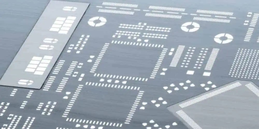
Material choice governs aperture edge sharpness, paste release characteristics, long-term stencil flatness, and resistance to the mechanical stress that step geometries amplify over a production run.
- 304 stainless steel: 304 stainless steel (HTA grade) is the industry standard for stepped foils. The High Tension Annealed process produces a fine, recrystallized grain structure with hardness above 370 HV. This elevated hardness is particularly important at step transitions, where cyclic stress concentrations from squeegee loading would progressively work-harden and eventually crack a lower-grade material. HTA stainless steel resists this failure mode over tens of thousands of print cycles, which is why it is specified by name in most step stencil procurement standards.
- Nickel-plated steel: Nickel-plated steel fills micro-surface irregularities with a thin nickel layer to lower friction and improve paste release without the cost of a fully electroformed stencil. It is a reasonable middle ground for applications where transfer efficiency matters but electroforming is not warranted by component pitch or volume.
- Pure nickel (electroformed): Pure nickel offers maximum transfer efficiency and should be reserved for the electroforming process where it is structurally appropriate. Its relative softness makes it impractical on high-cycle production lines where mechanical handling causes routine surface contact.
Choosing a Step Stencil Thickness Profile
There is a critical early design decision when it comes to matching the step stencil thickness profile to the component mix on the board. Common configurations used in production:
- 0.15 mm base / 0.10 mm step-down — The most widely used configuration. Well-suited for standard SMT boards carrying 0.4 mm pitch BGAs or QFNs in an otherwise conventional consumer layout.
- 0.20 mm base / 0.15 mm step-down — Used for paste-in-hole assemblies where through-hole barrels need substantial paste fill alongside standard 0.5 mm pitch surface-mount devices.
- 0.12 mm base / 0.08 mm step-down — High-density configurations requiring tight volume control for 0.3 mm micro-BGAs or 01005 passives. At T_step = 0.08 mm, aperture AR must be verified carefully, and Type 5 solder paste powder is typically required to satisfy the five-particle minimum rule per IPC J-STD-005A.
After settling on a profile, always recalculate area ratios for all apertures in the thinned zones before the design is finalized for tooling.
Surface Treatments That Matter More on Stepped Foils
Surface treatments that are optional on flat stencils become close to mandatory on stepped designs.
- Electropolishing: This passes the stencil through an electrochemical bath in which the foil acts as the anode. Current flow preferentially dissolves the peaks of surface microtopography, laser slag, burrs, and the stressed metal at step-transition edges, leaving behind a smoother, more uniform surface. On flat stencils, this is a useful enhancement; on stepped foils, it is effectively mandatory. The sharp vertical wall at a step transition is geometrically similar to a blade edge: if left unpolished, the squeegee catches it, generates a localized pressure spike, and either deposits an erratic paste bead at that location or gradually damages the blade edge. Electropolishing rounds this transition and allows the squeegee to traverse it cleanly over the stencil's entire service life.
- Nano-coating: It applies a hydrophobic polymer layer, typically 1–2 µm of silicon-fluorine compound, to the bottom surface and aperture walls. The mechanism is straightforward: by reducing the surface energy of the stencil, the coating lowers the adhesion force between the solder paste and stencil material. In step-down zones where area ratios are already compressed below comfortable margins, nano-coating provides measurable transfer efficiency improvement by allowing the paste column to shear cleanly from the wall without relying on print pressure alone. It also significantly reduces the rate at which paste wicks under the foil during printing, extending underside cleaning intervals and reducing the risk of smearing defects.
- Ultrasonic-resistant adhesive: This is a frame-level specification that matters more for stepped stencils than flat ones. Step designs trap more paste residue in recessed pockets and therefore require more aggressive cleaning cycles, often including ultrasonic baths, to prevent paste buildup from affecting print quality. Standard frame adhesives can delaminate under repeated ultrasonic exposure, progressively relaxing frame tension and degrading print registration. Specifying an ultrasonics-rated adhesive at the time of order protects stencil integrity through the full service life.
Why Engineers Order Step Stencils From JLCPCB?
For engineers who need professional-grade stepped foils without the lead time or MOQ constraints of traditional suppliers, JLCPCB offers a practical option. Custom step stencils start at $3 with no minimum order quantity, which makes step-stencil prototyping genuinely accessible without committing to production volumes. Build times can be as fast as 12 hours, with global shipping covering 180+ countries.
Technically, JLCPCB uses 304 HTA stainless base foils with laser-cutting tolerances down to ±0.003 mm. Engineers specify step depths, zone layouts, electropolishing, nano-coating, and ultrasonic-resistant frame adhesive directly through the instant quoting platform on Gerber or DXF upload, with no manual back-and-forth with an application engineer required.
Common Step Stencil Defects and How to Prevent Them
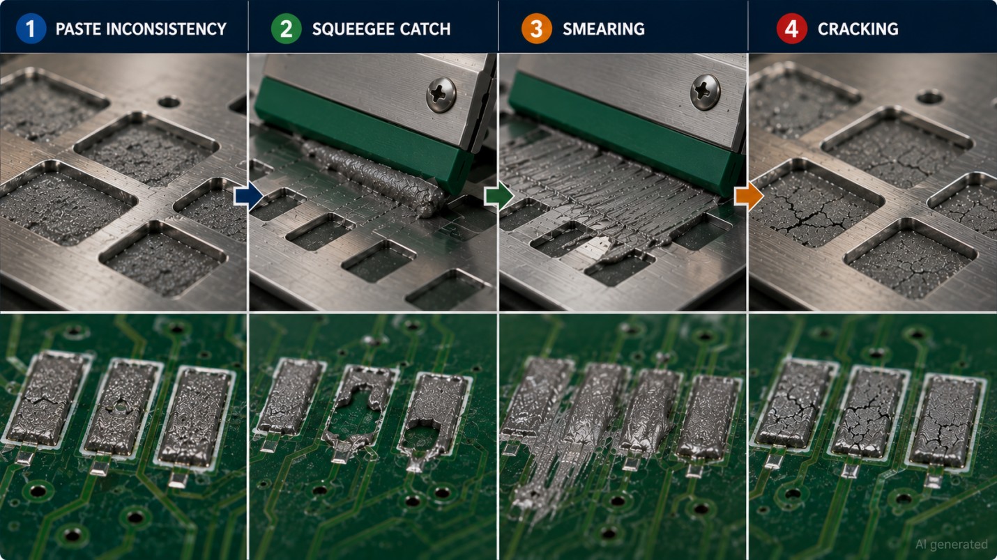
Inconsistent Paste Volume at Step Transitions
An aperture placed too close to the step boundary sits in the zone where squeegee blade pressure is inconsistent as it crosses the height change. Pads in this region end up with variable joint heights, solder starvation, or excess paste depending on which side of the step boundary they fall on.
Fix: Enforce ≥ 1.5–2.0 mm clearance between any active aperture and the nearest step edge. When board real estate is genuinely constrained, a micro-machined ramped transition instead of a sharp vertical step wall extends the pressure recovery zone and reduces the severity of the pressure drop.
Squeegee Skipping, Bouncing, or Catching at the Step
Unpolished, sharp step transition edge, and polyurethane or soft squeegee blade. The blade catches on the step-up boundary, skips past across nearby apertures, and degrades both the squeegee edge and the stencil surface over time.
Fix: Specify electropolishing to bevel and smooth step transition edges. Use rigid metal squeegee blades exclusively. On first production runs with a new step stencil, reduce print speed by 10–20% from the standard flat-stencil setting and adjust from there based on inspection results.
Paste Smearing Across the Step Boundary
Foil rebounds after the squeegee crosses the step. If the stencil doesn't maintain a tight, consistent gasket seal against the PCB surface, paste pools along the underside of the step edge and smears onto adjacent pads during board separation.
Fix: Reduce stencil separation speed. Slower separation usually restores gasketing at the step boundary. Increase underside cleaning frequency. Confirm step depth doesn't exceed 50% of base thickness, as deeper steps increase the rebound force on separation.
Cracking or Foil Fatigue at the Step Interface
Low-grade base material, oversized step depth, or sharp internal corners in the step zone geometry create stress concentration zones at the step boundary. Under continuous squeegee pressure, micro-cracks propagate, and frame tension degrades over the stencil's service life.
Fix: Use 304 HTA stainless steel or better. Keep step depth within the 50% limit. Specify radii on interior step zone corners rather than sharp 90° angles. Distributed stress geometry extends stencil life meaningfully on high-cycle lines.
Insufficient Paste Release in the Recessed Zone
In a step-down zone the foil is thinner, which actually aids release — so when the paste still refuses to let go, the cause is usually a genuinely small fine-pitch aperture (low area ratio from tiny L and W) made worse by rough, un-electropolished walls. Paste stays trapped inside the opening due to surface tension and wall friction.
Fix: Verify AR ≥ 0.66 for every aperture in step-down zones after step depth is finalized. Apply electropolishing plus nano-coating. If the area ratio still falls short, widen the aperture geometry, thin the zone further (a deeper step, within the 50% limit), or switch to a rounded/home-plate aperture shape.
For reference, the area ratio for rectangular apertures is:
AR = (L × W) / (2 × (L + W) × T_step) ≥ 0.66
Where L = aperture length, W = aperture width, and T_step = local stepped foil thickness.
FAQs About Step Stencil Design and Manufacturing
Q: Can step zones be placed on both sides of the same stencil?
Yes. They serve different purposes. Board-side step-downs ensure a tight gasket seal to prevent paste bleed. Squeegee-side step-ups add paste volume for larger components while keeping the board-contact surface perfectly flat.
Q: How does the solder paste powder type affect thin step-down zones?
Powder size must match the thinnest zone. Per IPC J-STD-005A, the smallest aperture must span at least five powder particles. Type 4 powder is marginal in a 0.08 mm zone. Use Type 5 for component pitches under 0.3 mm.
Q: Is it practical to use more than two thickness levels?
Rarely. Extra levels reduce foil tension and complicate the printing process. A single step (two levels) handles most mixed-pitch boards. Three levels are complex and require process validation before production.
Q: When should the area ratio be rechecked?
Recheck after any change to step depth, aperture geometry, or pad layout. A tiny 0.01 mm depth change can drop your Area Ratio below the IPC-7525B minimum of 0.66. Always check during design review before tooling.
Conclusion: Get Your Step Stencil Design Right the First Time
Step stencils solve real paste-volume mismatch problems that flat stencils simply cannot address. However, they only deliver clean results when your design strictly respects step depth limits, aperture clearance rules, and the correct manufacturing method.
On a stepped foil, design quality and manufacturing precision are compounded. A brilliant layout will still fail under poor process control, just as flawless manufacturing cannot save a poorly specified design. Both sides of the equation must be right.
To guarantee a perfect single-pass print run, check out the full specifications on the JLCPCB stencil page and upload your Gerber or DXF files for an instant online quote today.
Keep Learning
BGA Stencil Design: Apertures, Thickness & Tips
On a ball grid array, every solder joint hides underneath the package where you cannot see it, touch it, or easily rework it. That is exactly why BGA stencil design decides whether the board works: the paste you print is the paste you get, and a print that is slightly too heavy or too light turns into hidden bridges, voids, or starved balls that only an X-ray will reveal. Get the stencil right and the joints reflow clean the first time. Get it wrong and you are chasing intermittent faults after assemb......
Stencil Aperture Design: Geometry, Area Ratio & Tips
Key Takeaways Stencil aperture design controls paste volume, deposit shape, and print registration — it's the key controllable variable in SMT print quality. As per IPC-7525B, two math rules are non-negotiable: stencil area ratio ≥ 0.66 and stencil aspect ratio ≥ 1.5. Aperture geometry is component-dependent: 1:1 with pad for BGA, window-pane splits for QFN/BGA thermal pads, home-plate shapes for 0201/01005 chips, and modest reductions for fine-pitch QFP. Aperture reductions intentionally decrease the......
Red Glue Stencil: Types, Thickness & Ordering Guide
Key Takeaways A red glue stencil deposits adhesive dots under component bodies, not solder paste on electrical pads. Its main use is holding bottom-side SMD parts during wave soldering of through-hole leads. SMT red glue is commonly dyed red so operators can confirm each deposit during inspection. Printable adhesive families include epoxy, acrylic, and UV- or dual-cure materials. Glue stencils are commonly thicker than paste stencils because the dot must reach the component underside. A custom o......
DFN Package Guide: Footprint, Soldering & Stencil Tips
Key Takeaways What a DFN is: A DFN (Dual Flat No-Lead) package is a leadless chip-scale IC package with connection pads on two opposing sides of its underside, usually plus a central exposed thermal pad. Assembly requirements: DFN joints sit hidden under the body, so it needs reflow soldering with a stencil and X-ray or AOI inspection, not hand soldering. Design essentials: Follow IPC-7351 land patterns and IPC-7525 aperture rules, use a thinner stencil foil around 0.1-0.12 mm, and segment the thermal......
A Beginners Guide to Step-Up and Step-Down Stencils
As everyone knows, companies are moving down to 2nm, and electronics are at their peak right now. The component sizes of a PCB likewise drastically shrink during a ten-year period. From 1206, BGAs have shrunk to 0402, 0201, and even smaller. Due to the small size of the components and the requirement for high throughput, defects such as tombstoning, bridging, or poor connections may occur during the soldering process. To address these challenges, specialized stencil technologies such as step-up and st......
Design Guidelines for Industry-Standard Solder Stencil
Solder paste printing is one of the most important processes in PCB assembly, and the design of a stencil directly affects the quality of solder paste application. In a previous article, we discussed stencils and their types in detail. JLCPCB’s advanced stencil options, including step-up/step-down and nano-coated stencils, help engineers achieve higher printing accuracy and assembly reliability. In electronics hardware design, following proper design rules is just as crucial as having the right tools.......