
BGA Reballing Explained: Complete Process, Tools, Risks, and Best Practices
16 min
- BGA Reballing at a Glance (Quick Overview)
- What Is BGA Reballing and How Does It Work?
- Why Is BGA Reballing Necessary? Common Failure Causes
- BGA Reballing Process: Step-by-Step Professional Workflow
- Tools, Equipment, and Cost for BGA Reballing
- BGA Reballing vs Chip Replacement: Which Is Better?
- Common Risks in BGA Reballing and How to Avoid
- Best Practices: Reliable BGA Assembly at JLCPCB
- FAQ About BGA Reballing
- Conclusion
In modern electronics design, the Ball Grid Array (BGA) is the standard for high-performance silicon, enabling thousands of I/O connections in a tiny footprint. However, this density creates a "black box" scenario: connections are hidden, and defects like cold joints or thermal fatigue cracks are invisible to the naked eye. Unlike a QFP that can be fixed with a soldering iron, a failed BGA threatens the viability of the entire board.
BGA reballing is the critical solution to this problem. It is the precise process of removing a component, stripping old solder, and attaching a fresh grid of spheres to restore full electrical and mechanical integrity.
This guide covers the technical depths of the BGA reballing process - from the physics of the intermetallic bond to the specific thermal profiles required for success. We will also discuss how industrial-grade assembly standards at JLCPCB can mitigate these risks during initial manufacturing.
BGA Reballing at a Glance (Quick Overview)
| Item | Summary |
|---|---|
| What It Is | A repair process that removes old solder balls from a BGA chip and replaces them with new ones |
| When to Use It | When BGA joints fail due to thermal cycling, drop damage, or manufacturing defects |
| Success Rate | Typically 60%–90%, depending on chip condition, tools, and technician skill |
| Difficulty Level | High – requires professional equipment and experience |
| Typical Cost Range | USD $20–$150+ per chip, depending on size and complexity |
Engineer's Tip:
If the BGA failure is caused by PCB pad damage or internal chip defects, reballing will not fix the problem. In such cases, component replacement is the only reliable solution.
What Is BGA Reballing and How Does It Work?
BGA reballing is an electronics rework process where old solder balls are removed from a Ball Grid Array (BGA) component and replaced with new solder spheres to restore electrical and mechanical connections.
At a surface level, reballing seems like a simple mechanical replacement. However, for a PCB design engineer or SMT technician, understanding the physics is crucial. A BGA solder joint performs two functions: it provides an electrical path for signals and power, and it acts as a mechanical anchor.
The solder ball is not a rigid pillar; it is a compliant structure designed to absorb stress. During the operation of a device, the silicon die inside the chip generates heat. Silicon has a much lower Coefficient of Thermal Expansion (CTE) than the FR4 glass-epoxy material of the PCB. As the device heats up and cools down (thermal cycling), the PCB expands more than the chip. This mismatch creates shear stress, particularly on the solder balls located at the corners of the package - the points furthest from the neutral center (Distance to Neutral Point, or DNP).
When you perform a BGA reballing, you are essentially resetting the fatigue clock of the assembly. The process involves reforming the Intermetallic Compound (IMC) layer. The IMC is a thin layer formed where the tin in the solder reacts with the copper pad (forming Cu6Sn5). A joint without a proper IMC layer is weak (cold joint), but a joint with an IMC layer that is too thick becomes brittle. Reballing requires precise temperature control to ensure that the new spheres wet the pad and form a healthy IMC layer without damaging the delicate substrate.
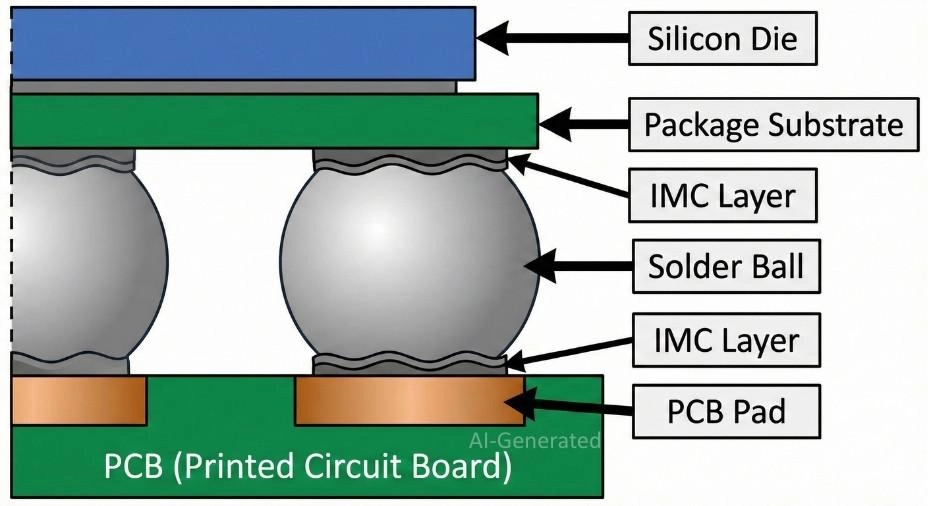
Figure: BGA package interconnects showing silicon die, solder ball grid array, and intermetallic compound layers.
At JLCPCB, we recognize the critical importance of BGA solder joint integrity. We employ advanced 3D X-ray inspection (AXI) in our SMT process to evaluate solder joint shape, voiding, and alignment across BGA assemblies, ensuring consistent quality and high manufacturing yield.

Why Is BGA Reballing Necessary? Common Failure Causes
Why go through the labor-intensive process of reballing instead of simply reflowing the existing part? Often, a simple reflow is insufficient because the solder alloy itself has degraded, or the original manufacturing process was flawed. Here are the primary technical drivers for a BGA reballing:
#1. Solder Joint Fatigue & Work Hardening
As mentioned regarding CTE mismatch, repeated thermal cycling causes the grain structure of the solder to coarsen. Eventually, micro-cracks initiate and propagate through the joint, leading to intermittent failures. Simply reheating the old, fatigued solder will not restore its ductility. The old alloy must be removed and replaced with fresh solder spheres to restore reliability.
#2. Oxidation and "Black Pad" Defects
Sometimes, a joint fails because of surface finish issues, such as "Black Pad" in ENIG (Electroless Nickel Immersion Gold) finishes, where the nickel corrodes before the gold is applied. This prevents proper wetting. Reballing allows the technician to inspect the component pads, clean away oxidation, and apply aggressive flux to attempt a better bond.
#3. Bridge Shorts and Solder Voids
During initial prototype assembly, if the stencil aperture was too large or the reflow profile was incorrect, adjacent balls might bridge, or large voids might form inside the ball. Reballing gives you a clean slate to correct these volume discrepancies.
#4. BGA Chip Salvage from Donor Boards
In times of silicon shortages, engineers often harvest high-value components (like FPGAs or GPUs) from damaged PCBs (donor boards). Once desoldered, the residual solder on the chip is uneven and oxidized. You cannot solder a pulled chip onto a new board without reballing it first to ensure planarity.
#5. Alloy Conversion (Lead-Free to Leaded)
This is common in the aerospace and defense sectors. Commercial Off-The-Shelf (COTS) components are typically Lead-Free (SAC305). However, for high-reliability applications where "tin whiskers" are a concern, engineers may require the BGA to be reballed with Leaded solder (Sn63Pb37), which is more ductile and resistant to whisker growth.
| Failure Mode | Description | Why Reflow Is Not Enough |
|---|---|---|
| Cold Solder Joint | Incomplete wetting where the solder did not flow across the pad. | Requires flux and fresh alloy to break surface tension and form a true metallurgical bond. |
| Head-in-Pillow (HiP) | The ball deformed but didn't merge with the paste on the PCB, looking like a head resting on a pillow. | The mating surfaces are oxidized. Fresh balls and flux are needed to clean and merge the connection. |
| Solder Bridging | Excess solder connecting two adjacent pads. | You must remove the excess material to clear the short; reballing ensures the remaining volume is consistent. |
| Intermittent Open | A crack that opens only when the board is hot (expanded). | The grain structure of the solder is fractured. Only replacing the ball restores mechanical strength. |
BGA Reballing Process: Step-by-Step Professional Workflow
Reballing is a precision art that balances thermal management with mechanical accuracy. Here is the technical workflow adopted by professional rework houses.
Step 1: BGA Component Removal (Desoldering Process)
The process begins with removing the BGA from the PCB. This cannot be done with a hand iron. You need a dedicated BGA Rework Station with split-vision optics and a controlled thermal profile.
● Thermal Profiling: The board must undergo a profile similar to the original reflow: Preheat, Soak, Reflow, and Cooling.
● Pre-heating: It is critical to heat the bottom of the PCB to approximately 100°C–120°C before applying top heat. This reduces the thermal delta, preventing the board from warping or delaminating.
● Removal: Once the solder reaches liquidus (approx. 217°C for SAC305), the vacuum pickup tool lifts the component vertically to avoid smearing the pads.
Step 2: Pad Cleaning and Site Preparation
Once the chip is off, the pads on both the PCB and the component will be covered in residual, uneven solder.
● Wicking: Apply a high-quality gel flux and use a copper desoldering braid (solder wick) with a flat-blade soldering iron. The goal is to remove the old solder until the pads are perfectly flat.
● Coplanarity: This is the most critical factor. If one pad has a slightly higher bump of residual solder than the others, the new ball will sit higher, preventing surrounding balls from making contact during the final reflow.
● Cleaning: Use Isopropyl Alcohol (IPA) and lint-free wipes to remove all flux residues. The surface must be pristine.
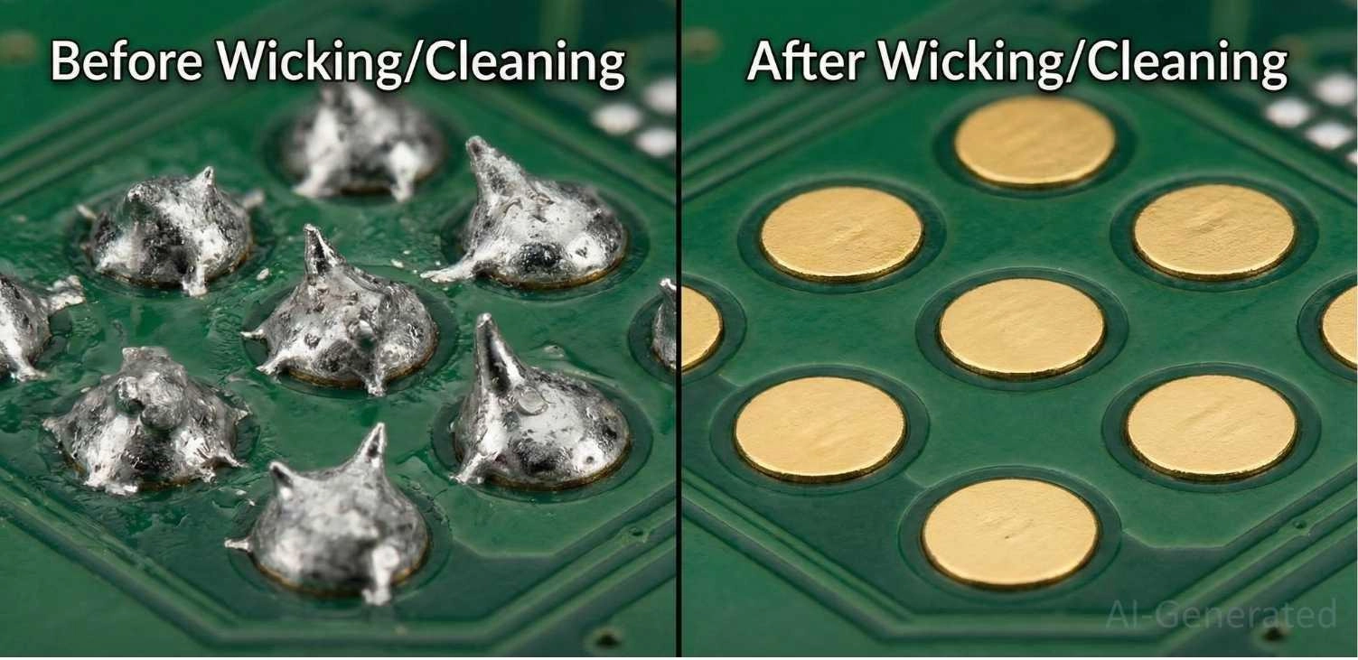
Figure: Comparison of BGA pads before and after solder wicking and cleaning for coplanarity.
Step 3: Stencil Alignment and Flux Application
To attach new balls, you need a way to hold them in place.
● The Jig: The component is placed in a reballing jig.
● Fluxing: A thin, uniform layer of tacky flux is applied to the component pads. If the layer is too thick, the balls will "float" and may merge during reflow. If too thin, they won't stick.
● The Stencil: A universal or dedicated BGA Stencil is aligned over the chip. The apertures of the stencil must align perfectly with the pads.
Step 4: Solder Ball Placement Techniques
● Solder Spheres: Thousands of pre-formed solder spheres are poured over the stencil.
● Selection: You must match the ball diameter to the component datasheet (e.g., 0.3mm, 0.45mm, 0.6mm, 0.76mm). Using the wrong size will lead to bridging or opening.
● Alloy: Choose between SAC305 (Lead-Free) or Sn63Pb37 (Leaded) based on the application requirements.
Step 5: Reflow Profile Control and Inspection
This step melts the new balls onto the component pads.
● Heat Application: This can be done in a reflow oven or carefully with a hot air wand.
● Self-Alignment: As the solder melts, surface tension becomes the dominant force. You will visually see the balls "center" themselves on the pads.
● Cooling: Allow the chip to cool naturally. Forced cooling can induce thermal shock and brittleness in the new joints.
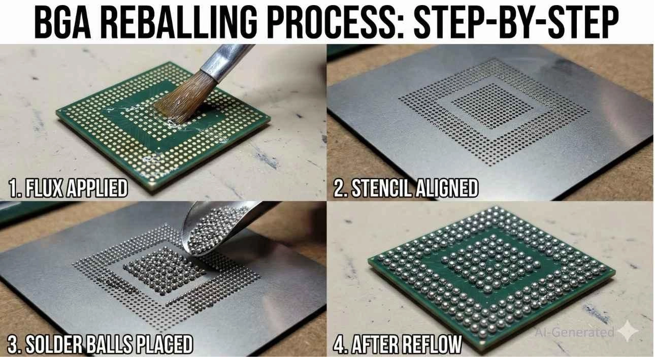
Figure: Step-by-step BGA reballing process showing fluxing, stenciling, ball placement, and post-reflow results.
Tools, Equipment, and Cost for BGA Reballing
Essential BGA Reballing Tools and Machines
Achieving a reliable reball requires specialized equipment. The cornerstone is a professional BGA Rework Station, equipped with bottom-side IR pre-heaters and top-side hot air or IR heating, along with a split-vision optical alignment system. Other essential tools include:
● Reballing Jigs and Stencils: Precision-cut steel stencils that match the exact ball pitch and array pattern of the specific IC.
● Solder Spheres and Flux: High-quality, perfectly spherical solder balls (SAC305 or Sn63Pb37) and specialized highly-tacky, no-clean or water-soluble flux.
● Desoldering Tools: Wide copper braids (solder wick) and temperature-controlled soldering irons with blade/chisel tips for pad preparation.
Manual vs Semi-Automatic Reballing Equipment
The choice of equipment heavily influences the success rate.
● Manual Equipment: Relies on hand-held hot air wands, universal stencils, and visual alignment. This method is highly dependent on operator skill, carries a higher risk of thermal damage, and is generally only suited for low-volume or hobbyist repairs.
● Semi-Automatic Equipment: Utilizes programmable thermal profiles to replicate the exact factory reflow curve. They feature automated vacuum pick-and-place and prism-based optical alignment to superimpose the BGA pads over the PCB footprint. This is the industry standard for EMS providers, ensuring repeatable, high-yield repairs.
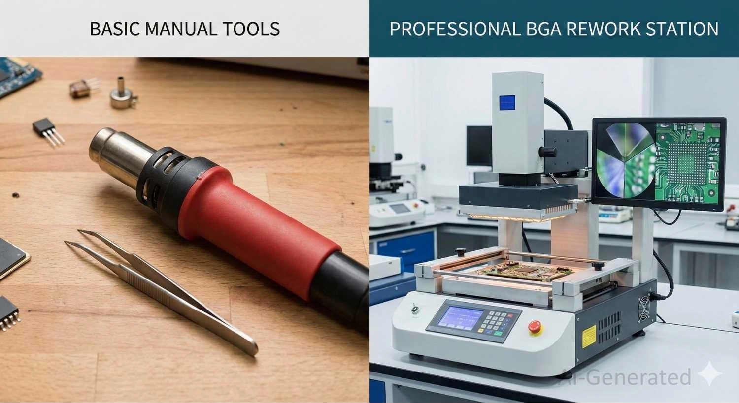
Figure: Comparison of manual hot-air tools versus a professional semi-automatic BGA rework station with optical alignment.
Typical BGA Reballing Cost and Time
The cost of reballing a BGA varies based on the component's pitch, pin count, and board volume. A single, complex FPGA might cost anywhere from $50 to $200+ for a specialized rework house to reball, not including the original diagnostic time.
The physical process itself typically takes an experienced technician 1 to 2 hours per chip, factoring in the slow thermal profiling, cooling, and meticulous cleaning stages.
BGA Reballing vs Chip Replacement: Which Is Better?
When Reballing Is Worth It
Reballing makes the most economic and technical sense when:
● High-Value Silicon: The component is a highly expensive CPU, GPU, or custom FPGA where the replacement cost far exceeds the labor cost of reballing.
● Obsolete Parts: The IC is out of production, and the only way to repair a legacy system is to harvest the chip from a donor board and reball it.
● Known Assembly Defects: The failure is purely mechanical (e.g., a cold joint or bridging from a poor initial reflow), and the silicon die is known to be fully functional.
When Full Replacement Is Recommended
A complete chip replacement is the superior choice when:
● Low Component Cost: If the IC costs $20, spending $100 on rework labor is inefficient. Buying a new component guarantees 100% mechanical and electrical integrity.
● Suspected Die Damage: If the component has suffered an over-voltage event, ESD damage, or shows signs of "popcorning" (moisture expansion damage), reballing will not fix the internal silicon failure.
● Pad Damage on the IC: If the component's substrate pads were ripped during the initial desoldering, the chip is permanently dead.
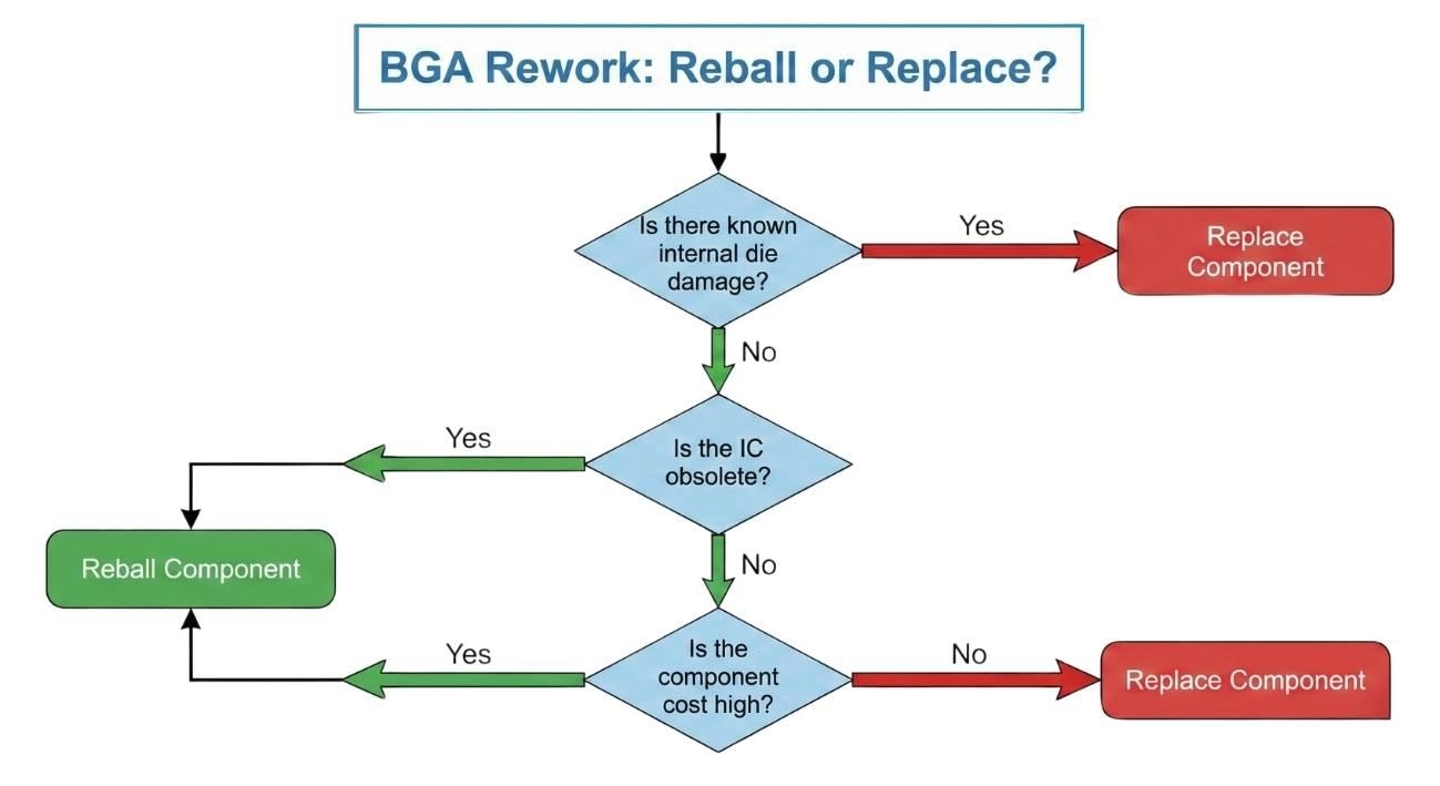
Success Rate Comparison
With a highly skilled operator and a semi-automatic rework station, BGA reballing can achieve an 80% to 90% success rate. However, installing a brand-new component on a properly prepared PCB yields a near 99% success rate. For mission-critical applications, replacing the chip is always the lower-risk option, provided the part is available.
Common Risks in BGA Reballing and How to Avoid
While BGA reballing saves components, it introduces risks that must be managed.
Thermal Damage
Every time a component is heated to reflow temperatures, the silicon die ages. There is a limit to how many thermal cycles a chip can endure before the internal wire bonds fail.
Precise thermal profiling is the only defense against "cooking" the chip.
Pad Lifting
During the cleaning phase, if the technician drags the soldering iron too aggressively or if the iron is too hot, the copper pads can be ripped off the delicate substrate laminate. Once a pad is lifted, the component is usually scrapped.
Popcorning and Moisture Sensitivity
Plastic-encapsulated microcircuits absorb moisture from the air. If a moisture-laden chip is rapidly heated, that water turns to steam, expanding and cracking the package - a phenomenon known as "popcorning."
Mitigation: Adhere strictly to IPC/JEDEC J-STD-033. Components should be baked in a drying oven (e.g., 125°C for 24 hours) to drive out moisture before any rework attempts.
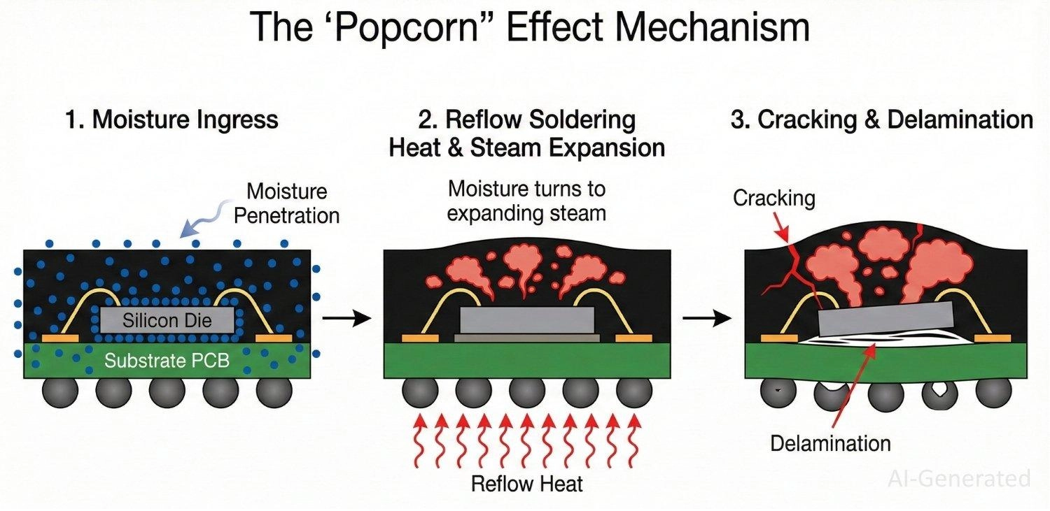
Figure: The Popcorn Effect in BGA packages caused by trapped moisture expansion during reflow.
Best Practices: Reliable BGA Assembly at JLCPCB
Reballing is a reactive measure - a fix for a problem that has already occurred. In the world of manufacturing, the goal is to prevent these defects entirely. This is where the choice of your PCBA provider becomes a strategic decision.
At JLCPCB, we employ industrial-grade safeguards to ensure BGA reliability during the initial assembly:
1. Precision Electro-Polished Stencils: We use high-precision pcb stencils with nano-coatings. This ensures the solder paste release is clean and consistent, providing the exact volume of solder required for each BGA pad, preventing the "starved" joints that eventually fail.
2. Automated Optical Inspection (AOI) & 3D X-Ray: Standard visual inspection cannot see under a BGA. JLCPCB utilizes inline X-Ray inspection to detect voids, bridges, and alignment issues before the board leaves the factory.
3. Reflow Profiling: We utilize multi-zone reflow ovens that allow for a controlled soak and peak temperature, tailored to the thermal mass of your specific board. This minimizes thermal stress and ensures optimal IMC formation.

- For critical embedded systems projects, relying on JLCPCB PCB assembly service ensures your BGAs are soldered with industrial-grade precision, significantly reducing the likelihood of field failures and the need for costly manual rework later.
FAQ About BGA Reballing
Q1: Can I reball a BGA using a heat gun and a handheld soldering iron?
Technically, it is possible, but highly discouraged for professional results. A handheld heat gun lacks the precise temperature control and airflow regulation needed. You risk overheating the die, warping the PCB, or blowing the solder balls out of position. A proper hot-air rework station with a pre-heater is the minimum requirement for reliable reballing.
Q2: What is the shelf life of a reballed BGA?
If done correctly, a reballed BGA can last as long as a factory-new component. However, the lifespan depends heavily on the cleaning process. If flux residues are left trapped under the balls, they can become corrosive over time or cause dendritic growth (electromigration), leading to failure months later. Thorough ultrasonic cleaning or the use of no-clean flux is essential.
Q3: How many times can a single BGA chip be reballed?
There is no hard rule, but the general industry consensus is limit it to 3 times maximum. Each reflow cycle stresses the internal silicon die and the substrate materials. Excessive thermal cycling increases the risk of internal delamination or wire bond failure, which cannot be repaired.
Q4: Is it better to use solder paste or solder balls for reballing?
Using solder balls is the industry standard and provides superior consistency. Solder paste reballing (smearing paste over a stencil) is faster but prone to issues; the flux in the paste outgasses, creating voids (air bubbles) inside the new bump. Solid solder spheres ensure 100% metal density and consistent height across the array.
Q5: Why do some engineers reball new chips with leaded solder?
This is often done for high-reliability industries like avionics or deep-sea exploration. Standard Lead-Free (SAC305) solder is more brittle and requires higher processing temperatures. Leaded solder (Sn63Pb37) is softer and more ductile, making it better at absorbing shock and vibration without cracking. Engineers may buy standard lead-free parts and reball them with leaded solder to increase mechanical reliability in harsh environments.
Q6: Can BGA Reballing Be Done at Home?
BGA reballing requires specialized industrial equipment and skills, so it is not suitable for home repair. At-home attempts usually result in permanent damage.
Conclusion
BGA reballing is a sophisticated procedure that sits at the intersection of metallurgy, physics, and manual dexterity. It is an essential skill for repair technicians and engineers dealing with high-value component salvage or legacy hardware repair. However, it is fraught with risks like thermal damage and pad lifting.
Understanding the root causes of BGA failure - thermal fatigue, oxidation, and process defects - empowers engineers to design more robust boards. Ultimately, the best solder joint is the one that is formed the first time. By partnering with quality manufacturers and adhering to strict design guidelines, you can ensure the longevity of your embedded systems.
Popular Articles
• Common PCB Assembly Methods and Soldering Techniques Explained
• What Is BGA Void? Causes, IPC Limits, and Solutions
• SMD Soldering Tools You Need: Complete Guide from Beginner to Pro
• Reflow Soldering: Everything You Need to Know
• SMT Assembly Process Explained and Equipment Used: A Step-by-Step Guide to PCBA Manufacturing
Keep Learning
Common PCB Assembly Methods and Soldering Techniques Explained
Whether you're designing your first prototype or scaling up to production, understanding PCB assembly methods and soldering techniques is crucial to achieving reliable, high-performance circuit boards. Modern PCBA primarily relies on Surface Mount Technology (SMT) and Through-Hole Technology (THT)—each offering unique advantages for component density, durability, and manufacturability. In this guide, we'll break down the major PCB assembly methods, key soldering techniques such as reflow and wave sold......
12 Professional Soldering Tips and Tricks Every Beginner Should Know
Soldering is not merely "gluing" metal; it is a metallurgical process that creates an intermetallic compound (IMC). This molecular bond ensures the electrical and mechanical integrity of your device. A poor joint might pass a quick visual check but will inevitably fail under vibration or thermal stress, leading to "ghost" bugs and hardware failures. These soldering tips and tricks focus on practical, repeatable techniques used in professional electronics soldering—from correct heat transfer and flux u......
Solder Melting Point Guide: Chart, Alloy Types, and Reflow Considerations
In the precise world of electronics manufacturing, a difference of just a few degrees can mean the distinction between a perfect, reliable solder joint and a catastrophic "cold" joint failure. While many hobbyists view soldering simply as "melting metal to stick things together," professional PCB assembly requires a nuanced understanding of thermodynamics. The solder melting point is not simply a single value listed in a datasheet; it is a decisive limit that determines the choice of components, the s......
The Ultimate Guide to Solder Flux: Everything You Should Know Before Soldering PCB
Soldering is needed to make almost all electronic devices. Adding solder alone won't make a joint that is strong, clean, and sound from a metallurgical point of view. Solder flux is a very important part of the process that comes in here. If you want to do your job better and make it more reliable, you need to know a lot about soldering flux, whether you're an engineer, a professional technician, or just a hobbyist. This article goes into a lot of detail about solder flux, including what it is, how it......
Flex PCB Assembly Guide: Process, Challenges, and Solutions
Flexible Printed Circuit Boards (Flex PCBs) are the foundational technology enabling the compact, innovative design of modern electronics. Because of their ability to bend and fold, they power devices from smart wearables to compact medical instruments where traditional rigid printed circuit boards (Rigid PCBs) can't be used. Achieving a functional electronic circuit from the raw plastic film demands special expertise, with flexible PCB assembly (FPCA) representing the crucial final step in this trans......
SMD Rework Guide: Tools, Temperatures, and Techniques That Prevent PCB Damage
From replacing a burned regulator to correcting wrong component values or removing solder bridges on fine-pitch ICs, SMD rework is an essential skill in electronics manufacturing and prototyping. It allows engineers to repair assembly defects, implement design changes, and recover valuable PCBs without the cost and delay of building new boards. In this guide, you will learn: What SMD rework is Common rework scenarios Tools and temperatures Safe removal and installation Package-specific techniques Real......