TSSOP Package Guide: Dimensions, Pitch, Footprint & SMT Soldering
20 min
- TSSOP Package Basics
- TSSOP Dimensions & Pitch
- TSSOP vs SOIC, SSOP, MSOP & QFN
- TSSOP Footprint & Land Pattern Design
- TSSOP SMT Assembly & Soldering
- Inspection & Rework
- FAQ about TSSOP Packages
Key Takeaways
Lead span, not body width: Build the footprint from the lead span (6.4 mm or 8.1 mm tip to tip), not the 4.4 mm or 6.1 mm body width.
MSOP vs TSSOP: Check the width in the drawing before reusing a footprint: MSOP-8 and TSSOP-8 share pitch and body length, and some vendors label a 3.0 mm-wide package TSSOP8.
Mask dams: A standard TSSOP footprint leaves a 0.20 mm pad gap: enough for solder mask dams on 1 oz copper, no margin on 2 oz, and no dams on JLCPCB flex boards.
Thermal pad: On HTSSOP, fill and cap the vias in the exposed pad and split the stencil aperture into windows.
Defects: Most TSSOP defects are bridges and lifted leads, so control paste volume and keep parts in their original packaging until placement.
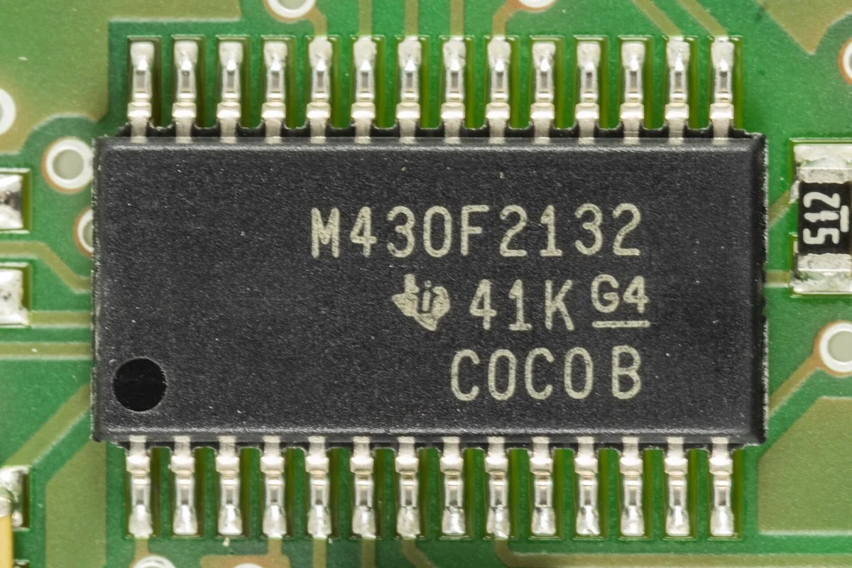
Figure: A 28-pin TSSOP (TI MSP430F2132) soldered on a PCB. Photo: Raimond Spekking, CC BY-SA 4.0, via Wikimedia Commons (cropped)
TSSOP stands for Thin Shrink Small Outline Package. The easiest way to picture it is as an SOIC with the lead pitch cut from 1.27 mm to 0.65 mm or 0.5 mm, and the height capped at 1.2 mm. It's a common choice for op-amps, logic, LDOs, DC-DC controllers, sensor interfaces and small MCUs: parts that need to save board space without going to a leadless package.
The leads stay visible, so you can check every joint under magnification and rework it with an ordinary soldering iron. At 0.5 mm pitch, though, the margins are thin, and many TSSOP assembly problems start at the footprint rather than in the reflow oven.
| Parameter | Typical TSSOP value |
|---|---|
| Lead pitch | 0.65 mm (most common) or 0.5 mm |
| Body width | 4.4 mm or 6.1 mm |
| Overall width (lead tip to lead tip) | 6.4 mm or 8.1 mm |
| Max package height | 1.2 mm |
| Common pin counts | 8 to 56 |
| JEDEC reference | MO-153 |
TSSOP Package Basics
Structure and pin counts
A TSSOP has two rows of gull-wing leads along the long sides of a plastic body. Each lead bends out and down so its foot sits flat on the pad, with a heel and a toe where solder fillets form. The leads are only about 0.1 to 0.2 mm thick, which makes them easy to solder and also easy to bend.
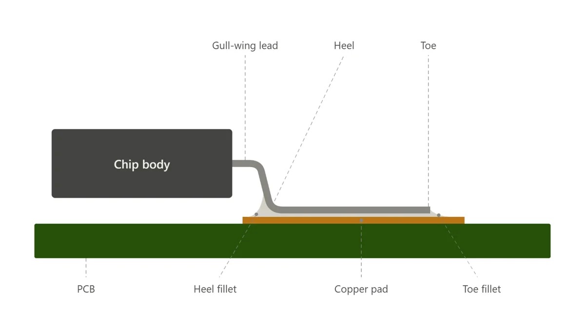
Figure: Side view of a gull-wing lead, showing where the heel and toe fillets form
At 0.65 mm pitch, the common pin counts are 8, 14, 16, 20, 24 and 28. Higher pin counts often use 0.5 mm pitch. Pin count alone doesn't define the package, though. For example, TI's 38-pin DBT package has a 4.4 mm-wide body with 0.5 mm pitch, while its 38-pin DAP HTSSOP uses 0.65 mm pitch on a body about 6.1 mm wide.
Identifying pin 1
Pin 1 is marked with a molded dot or dimple, and on some packages the edge along the pin-1 side is also beveled. Viewed from the top, pins are numbered counterclockwise: pin 1 is at the top-left, the count runs down the left side, then back up the right. On a TSSOP-20, pin 20 sits directly across from pin 1.
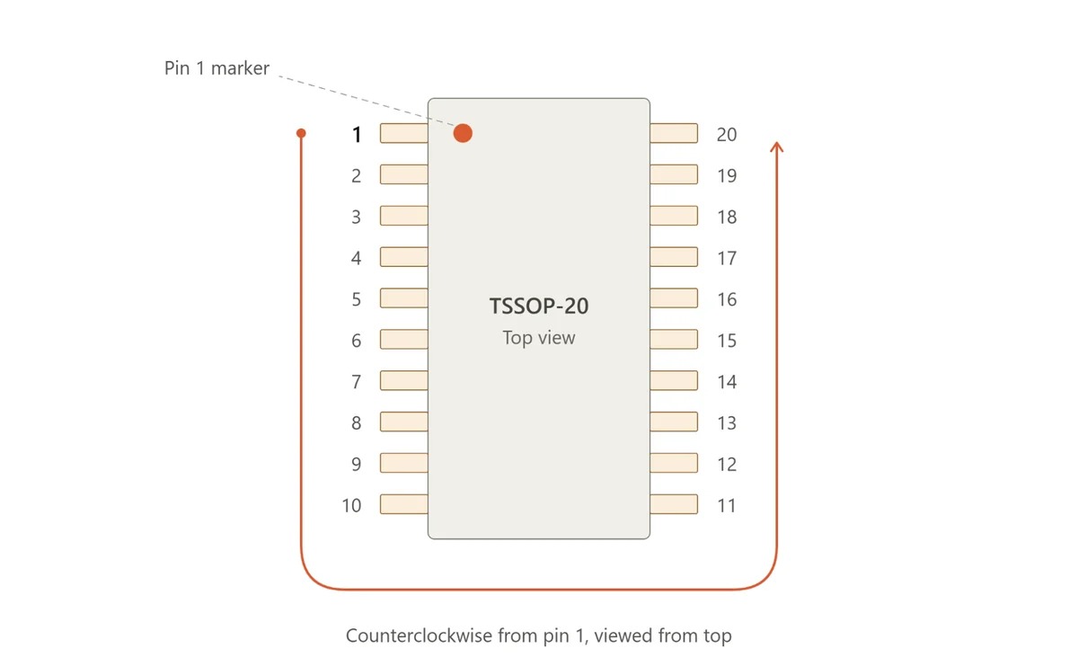
Figure: TSSOP-20 pin numbering, counterclockwise from the pin 1 marker when viewed from the top
Two details catch beginners. First, some bodies carry round ejector-pin marks from molding that look like a pin-1 dot. When in doubt, check the marking diagram in the datasheet. Second, the silkscreen pin-1 marker should sit outside the component outline, so it's still visible after the part is placed. It also matters at assembly: when the placement file and the silkscreen disagree, JLCPCB places parts by the silkscreen, and Confirm Parts Placement ($0.45) lets you check pin 1 in the production file before assembly starts.
TSSOP vs TSOP
TSOP is a different package family used mainly for memory. The Type I version has its leads on the short edges; a TSOP-48 Type I, for example, is about 12 mm × 20 mm. The two are not interchangeable, and searches for "TSOP-48" and "TSSOP-48" return completely different parts.
Variants and naming
The main variant is the HTSSOP, also called TSSOP-EP or, at TI, PowerPAD TSSOP. It has an exposed metal pad on the underside that is soldered to the PCB for heat dissipation. Vendors use their own package codes: TI's PW is the standard 4.4 mm TSSOP, PWP is its HTSSOP version, and DGG is the 6.1 mm-body TSSOP at 0.5 mm pitch. Analog Devices uses RU.
Footprint names in the LCSC/EasyEDA library spell out the key dimensions, as in TSSOP-20_L6.5-W4.4-P0.65-LS6.4: body length, body width, pitch and lead span. Whatever the name says, the mechanical drawing in the datasheet is what the footprint should be built from.
TSSOP Dimensions & Pitch
The most common dimension mistake is confusing body width with overall width. The 4.4 mm figure measures the plastic body only. From lead tip to lead tip, the same package is about 6.4 mm wide, and the 6.1 mm-body family is about 8.1 mm wide. A footprint built around the body width puts the pads far too close together.
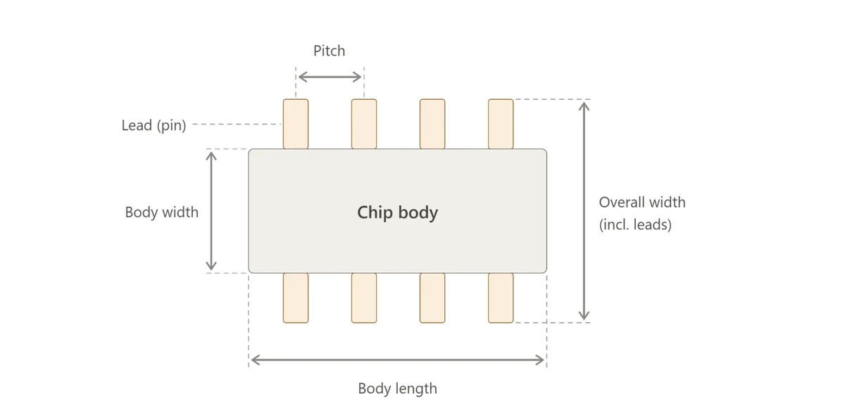
Figure: Body width vs overall width. The pad rows follow the overall width across the leads
The 4.4 mm body mostly uses 0.65 mm pitch up to 28 pins, and the 6.1 mm body mostly uses 0.5 mm pitch for 48 and 56 pins. The values below are representative nominal dimensions from vendor drawings based on JEDEC MO-153; individual parts can differ, so check the drawing for your exact part. For example, NXP's TSSOP-20 outline gives a 6.5 mm × 4.4 mm body at 0.65 mm pitch with a 1.2 mm maximum seated height. TI's DGG48 is 12.4–12.6 mm long, with a 6.0–6.2 mm body and 7.9–8.3 mm across the leads, at 0.5 mm pitch.
| Package | Pitch (mm) | Body length (mm) | Body width (mm) | Overall width (mm) | Max height (mm) |
|---|---|---|---|---|---|
| TSSOP-8 | 0.65 | 3.0 | 4.4 | 6.4 | 1.2 |
| TSSOP-14 | 0.65 | 5.0 | 4.4 | 6.4 | 1.2 |
| TSSOP-16 | 0.65 | 5.0 | 4.4 | 6.4 | 1.2 |
| TSSOP-20 | 0.65 | 6.5 | 4.4 | 6.4 | 1.2 |
| TSSOP-24 | 0.65 | 7.8 | 4.4 | 6.4 | 1.2 |
| TSSOP-28 | 0.65 | 9.7 | 4.4 | 6.4 | 1.2 |
| TSSOP-38 | 0.5 | 9.7 | 4.4 | 6.4 | 1.2 |
| TSSOP-48 | 0.5 | 12.5 | 6.1 | 8.1 | 1.2 |
| TSSOP-56 | 0.5 | 14.0 | 6.1 | 8.1 | 1.2 |
Note that TSSOP-14 and TSSOP-16 share the same 5.0 mm body length. Some vendors also specify a lower maximum height of 1.1 mm or 1.0 mm, which matters under shield cans or in thin enclosures.
TSSOP vs SOIC, SSOP, MSOP & QFN
Many ICs offered in TSSOP are also sold in at least one of these packages, so the choice usually comes up during part selection.
| Package | Pitch (mm) | Typical body width (mm) | Max height (mm) | Common pin counts | Hand soldering |
|---|---|---|---|---|---|
| SOIC | 1.27 | 3.9 / 7.5 | 1.75–2.65 | 8–28 | Easy |
| SSOP | 0.65 (0.635 for QSOP) | 5.3 (3.9 for QSOP) | 2.0 | 8–38 | Moderate |
| TSSOP | 0.65 / 0.5 | 4.4 / 6.1 | 1.2 | 8–56 | Moderate |
| MSOP | 0.65 / 0.5 | 3.0 | 1.1 | 8–16 | Moderate to hard |
| QFN | 0.5 / 0.4 | 3×3 to 7×7+ | Varies (often 0.8–1.0) | 8–64+ | Hard |
With its 1.27 mm pitch, SOIC is the easiest of these to assemble and rework when board space isn't tight. SSOP matches TSSOP's pitch but is thicker and wider. TSSOP fits designs where height and area both matter but visible joints are still wanted. MSOP suits 8 to 10-pin parts where a TSSOP-8 is still too big. QFN is the next step down in size.
TSSOP vs SOIC
A TSSOP takes roughly half to two-thirds of the board area of a narrow-body SOIC package with the same pin count. A TSSOP-16, for example, measures 5.0 × 6.4 mm across its leads, against 9.9 × 6.0 mm for an SOIC-16, and sits about a third lower, at 1.2 mm maximum height against 1.75 mm. The cost is pitch. With typical 0.6 mm pads at 1.27 mm pitch, an SOIC footprint leaves about 0.67 mm between pads, more than three times the 0.20 mm gap on a standard TSSOP footprint, so paste volume and mask dams matter much less. Many logic and analog parts are sold in both packages, which makes the choice a trade between board area and assembly margin.
TSSOP vs MSOP
This pair is a common source of footprint mismatches. An MSOP-8 and a TSSOP-8 share the same 0.65 mm pitch and the same 3.0 mm body length. The MSOP-8, however, is 3.0 mm wide and about 4.9 mm across the leads, while the TSSOP-8 is 4.4 mm wide and about 6.4 mm across. TI also sells MSOP under the name VSSOP, which adds to the confusion. Some vendors go the other way: NXP and Nexperia list a 3.0 mm-wide, MSOP-sized package as TSSOP8 (SOT505-2), so "TSSOP-8" in a BOM or parts library doesn't guarantee a 4.4 mm body.
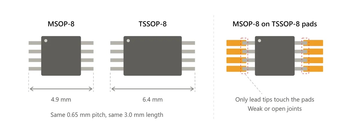
Figure: MSOP-8 vs TSSOP-8 width comparison and footprint mismatch
An MSOP placed on a TSSOP-8 footprint only reaches the inner ends of the pads, leaving weak or open joints. A TSSOP placed on an MSOP footprint overhangs the pads. If a part "almost fits," measure its overall width before blaming the reflow profile.
TSSOP vs QFN
Many ICs come in both packages. The QFN version is much smaller: Nexperia's 74HC595 in DHVQFN16 measures 2.5 × 3.5 mm, against 5.0 × 6.4 mm for the TSSOP-16 version across its leads. It also has lower lead inductance and conducts heat better through its exposed pad. In exchange, its joints are hidden: the thermal pad needs X-ray to inspect, and QFN soldering or rework by hand needs hot air. TSSOP joints can be checked by eye and touched up with an iron, which is why it's often chosen for prototypes and lower-volume builds. Switching packages means a layout change, so the decision is best made early.
TSSOP Footprint & Land Pattern Design
Pad dimensions
Start from the manufacturer's land pattern or from IPC-7351, as with any PCB footprint. TI's example layout for the 16-pin PW package uses 1.5 mm × 0.45 mm pads at 0.65 mm pitch, with the two pad rows 5.8 mm apart. The 0.5 mm-pitch DGG package uses 0.3 mm pads of the same length, with rows 7.5 mm apart. The pads extend past both the toe and the heel of the lead so fillets can form at each end.
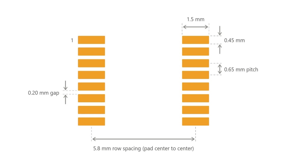
Figure: TSSOP-16 land pattern based on TI's PW example layout, with a 0.20 mm gap between pads
In both cases the gap between pads works out to the same number: 0.65 − 0.45 = 0.20 mm, and 0.5 − 0.30 = 0.20 mm. That figure matters in the next section.
Solder mask dams at fine pitch
A solder mask dam is a thin strip of mask between neighboring pads that blocks solder from bridging. The alternative, gang relief, opens the mask over the whole row of pads and leaves nothing to stop a bridge. For signal pads, TI's drawings mark non-solder-mask-defined (NSMD) pads as the preferred option.
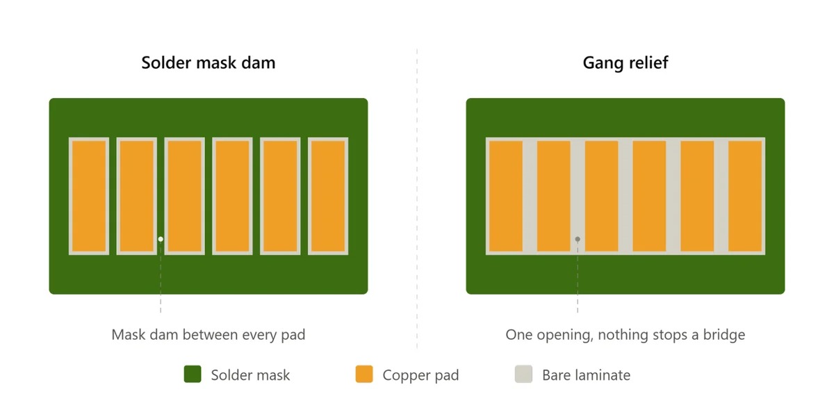
Figure: Solder mask dams between pads (left) vs a single gang relief opening (right)
For manufacturability and yield in volume production, JLCPCB recommends pad gaps of at least the following where solder mask dams need to stay. On 1 oz copper: 0.13 mm for green, red, yellow, blue and purple mask, and 0.15 mm for black and white. On 2 oz copper: 0.20 mm for any color. On 1 oz copper, these values leave some margin above the minimum pad spacing in JLCPCB's PCB capabilities: 0.10 mm, or 0.13 mm for black and white.
At JLCPCB, solder mask is exposed with LDI, so mask openings can be made 1:1 with the pads, with zero expansion per side.
Applied to a standard TSSOP footprint with its 0.20 mm copper-to-copper gap, a 1 oz board meets the recommendation in any color. A 2 oz board sits exactly on the 0.20 mm recommendation, at 0.65 mm pitch as well as 0.5 mm, with no extra margin. If the board needs heavier copper, confirm with the fab before the layout is frozen.
Flex boards follow a different rule: per JLCPCB's flex PCB capabilities, mask dams narrower than 0.5 mm are removed, so a TSSOP footprint with a 0.20 mm pad gap ends up with no dams at all. On flex, bridging has to be controlled through the stencil instead. If the flex board carries fine-pitch parts, mention them in the order remarks so they're visible during engineering review.
HTSSOP exposed pad and thermal vias
The exposed pad is the HTSSOP's main heat path, and thermal vias carry that heat into the inner and bottom copper. Datasheet examples typically place 0.2 to 0.3 mm vias on a grid of roughly 1.0 to 1.3 mm.
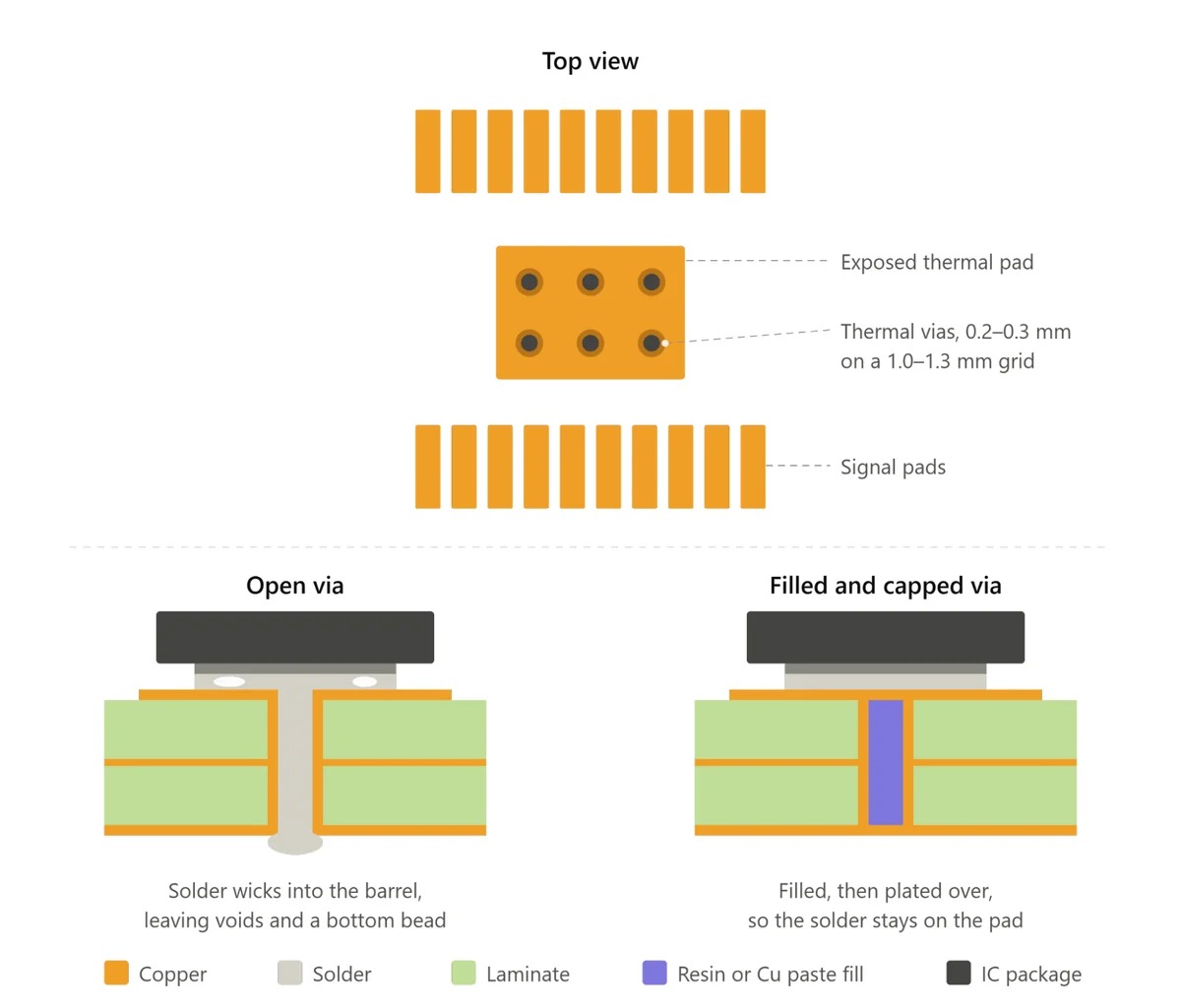
Figure: HTSSOP thermal via layout (top), and an open via vs a filled and capped via in the exposed pad (bottom)
Open vias in the pad pull solder down the barrel during reflow. The result is voids, starved joints, and sometimes solder beads on the bottom side of the board. TI recommends that vias under paste be filled, plugged or tented. At JLCPCB, vias that sit inside a soldermask opening can't be ink-plugged, but they can be filled with epoxy or copper paste and plated over. On boards with 6 or more layers, epoxy-filled and capped vias are the default, at no extra cost. If the design has tighter thermal requirements, the copper-paste option, with a thermal conductivity of 8 W/(m·K), can improve heat transfer to some extent.
TSSOP footprint checklist
- Build the footprint from the mechanical drawing of the exact part number, not from the package name.
- Confirm pitch, body width and overall lead span. The pad rows are set by lead span, not body width.
- Start from the manufacturer's land pattern or IPC-7351.
- Check that the MSOP vs TSSOP and 4.4 mm vs 6.1 mm variants match the part on the BOM.
- Compare the pad-to-pad gap with the fab's recommended solder mask dam spacing for your copper weight and mask color.
- Run a DFM check on the Gerbers, such as the free JLCDFM, to catch mask dams too narrow to hold.
- For HTSSOP, include the exposed pad, the thermal vias and a via treatment.
- Place the silkscreen pin-1 marker outside the body outline.
TSSOP SMT Assembly & Soldering
Stencil and solder paste
An SMT stencil about 0.12 to 0.13 mm thick is typical for 0.5 mm-pitch TSSOP; TI's example stencil for the DGG package assumes 0.125 mm. Reducing aperture width by about 10% from the pad width is a common starting point. The final value should follow the component vendor's stencil recommendation and the assembler's process. TI also notes that laser-cut apertures with trapezoidal walls and rounded corners can improve paste release. Too little paste opens up any lead that sits slightly high, and too much paste bridges. At 0.5 mm pitch there isn't much room between the two.
HTSSOP stencil windowing
Don't print a solid block of paste on the exposed pad. A thick layer lifts the package as it melts, pulls the outer leads off their pads, and traps flux gas that turns into voids. Split the aperture into a grid of windows covering roughly 50 to 70% of the pad, and keep paste off the via locations. If the datasheet gives a coverage figure, use that one.
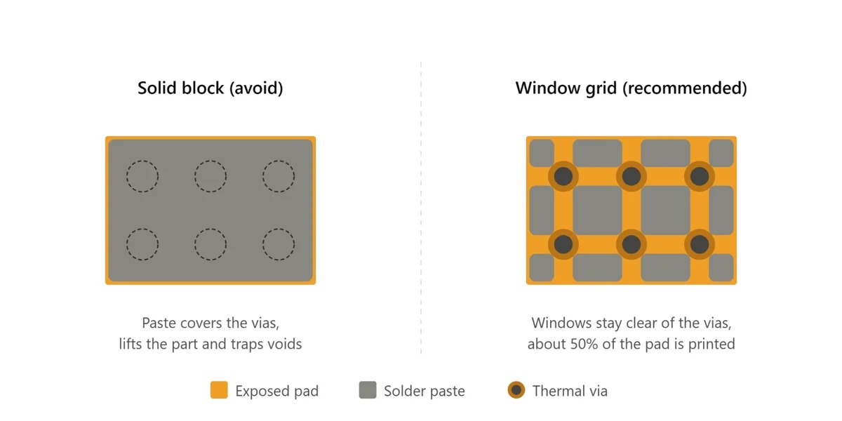
Figure: HTSSOP stencil apertures: a solid block (left) vs windows that keep paste off the vias (right)
Placement, reflow and MSL
For modern pick-and-place machines, 0.5 mm pitch is routine, and a standard SAC305 reflow profile works for TSSOP. The usual problems are bent leads and poor paste prints.
According to JLCPCB's PCB assembly capabilities, Economic PCBA handles IC pitches down to 0.4 mm, so a TSSOP at either pitch won't push a prototype into Standard PCBA. That matters on a small order, where fixed fees make up much of the prototype PCB assembly cost and Standard PCBA's are higher. Standard PCBA does add solder paste inspection (SPI), which Economic doesn't include.
Many TSSOP parts are rated MSL 1, but plenty are MSL 3, so check the reel label. J-STD-033 groups bake times by body thickness, and TSSOP falls into the thinnest group (1.4 mm or less), but the exact time still depends on the part's MSL level and how long it has been exposed. Standard tubes and tape-and-reel packaging aren't rated for a 125°C bake, so parts either get a long low-temperature bake or are moved to heat-resistant trays. That transfer is a common moment for leads to get bent.
Common defects
Bridging is one of the most common TSSOP defects. It usually comes from excess paste, a missing mask dam, or a shifted print. Insufficient wetting points to oxidized leads, old paste or low paste volume.
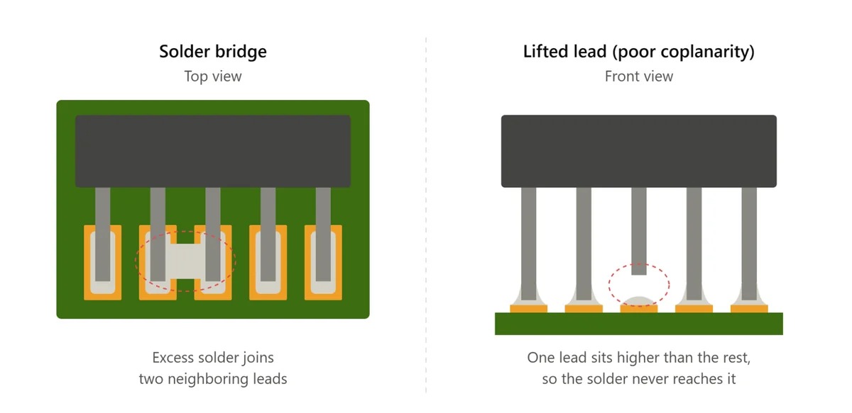
Figure: A solder bridge between neighboring leads (left) and a lifted lead caused by poor coplanarity (right)
Lifted leads and poor coplanarity are the defects most specific to TSSOP. Package drawings typically specify lead coplanarity within 0.10 mm, and a lead that sits 0.1 mm too high may barely touch a 0.12 mm paste deposit. Dropped reels, parts sliding in tubes, manual repacking and tray transfers can all push leads out of that range. Keeping parts in their original packaging until placement prevents most of it, and placement machines with lead inspection catch much of the rest.
Inspection & Rework
Gull-wing joints are visible, so AOI handles most TSSOP inspection, and 3D AOI makes lifted leads much easier to catch. The HTSSOP exposed pad is the exception: checking for voids underneath it takes X-ray. Void acceptance limits are usually set by the customer or the device vendor.
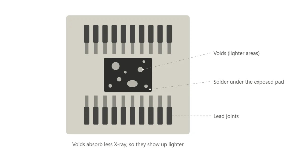
Figure: Illustration of voiding under an HTSSOP exposed pad as it appears in an X-ray image
Bridges and single bad joints are usually fixed by drag soldering, using plenty of flux, a hoof or chisel tip, and solder wick to clear the excess. For SMD rework on an HTSSOP, use hot air or a preheater: the soldered exposed pad holds the part down, so heating the leads alone won't free it.
Coplanarity problems leave a recognizable pattern: opens clustered at one corner or along one side, with no toe fillet on the affected leads. If several boards show the same pattern on parts from the same reel, suspect the components before the process. A slightly high lead can usually be reflowed with extra flux and a little solder. A visibly bent lead is better replaced than bent back.
FAQ about TSSOP Packages
Q: How do I choose the correct TSSOP footprint?
Start from the datasheet's mechanical drawing and recommended land pattern, not the package name. Check pitch, body width, overall lead span and, for HTSSOP, the exposed pad size before creating or selecting a footprint.
Q: What is the difference between TSSOP and SSOP?
They share the 0.65 mm pitch, but SSOP is taller (up to 2.0 mm) and usually wider (5.3 mm body). Their footprints are not interchangeable.
Q: Is TSSOP smaller than SOIC?
Yes. A TSSOP-16 takes 5.0 × 6.4 mm of board area across its leads, against 9.9 × 6.0 mm for a narrow-body SOIC-16, and its 1.2 mm maximum height is about a third lower than SOIC's 1.75 mm. The trade-off is the finer 0.65 mm pitch, which leaves less room for paste and mask dams between pads.
Q: Can you hand solder a TSSOP package?
Yes. Drag soldering with good flux works well at 0.65 mm pitch and is manageable at 0.5 mm with magnification. HTSSOP parts need hot air or a hot plate for the exposed pad.
Q: Why doesn't my MSOP chip fit my TSSOP footprint?
The two packages share pitch and body length but not width. An MSOP-8 measures about 4.9 mm across the leads and a TSSOP-8 about 6.4 mm, so the MSOP's leads fall short of the pads.
Q: How do I prevent solder bridging on 0.5 mm pitch TSSOP?
Keep mask dams between the pads, check the gap against the fab's recommended spacing for your copper weight and mask color, and start with a slightly reduced stencil aperture.
Q: Why is there voiding under my HTSSOP thermal pad?
Usually a solid paste print, open vias pulling solder away, or trapped flux gas. Windowed apertures and filled, capped vias fix most cases.
Q: Why do TSSOP pins bridge on my flex PCB when the same footprint works on a rigid board?
Flex boards usually lose their mask dams. JLCPCB removes flex mask dams narrower than 0.5 mm, so a TSSOP footprint ends up with nothing between its pads, and any excess paste can bridge. In after-sales cases we've reviewed, this showed up as bridged pins on the same fine-pitch parts across several boards in one order. On flex, check the pad gap against the flex capabilities before layout, and mention the fine-pitch parts in the order remarks so the stencil can be adjusted.
Conclusion: TSSOP Packages
A TSSOP is small enough for a dense board and still leaves joints you can see and touch up by hand. Most of the failures covered here start before the board reaches the oven: a footprint built from the part name instead of the drawing, body width mistaken for lead span, mask dams with no margin, or open vias under an HTSSOP pad. Bent leads are the main exception, and they come from handling, not from the reflow profile.
The JLCPCB parts library stocks a wide range of TSSOP parts, and each part page links to its datasheet, so you can check the package drawing before you commit a footprint. For PCBA orders, JLCPCB's PCB assembly service includes an engineering review before production that can catch some footprint and polarity issues, and Confirm Parts Placement lets you check pin 1 in the production file yourself.

Economic PCBA handles IC pitches down to 0.4 mm
Confirm Parts Placement lets you check pin 1 before assembly
Run a free JLCDFM check for solder mask dams too narrow to hold
Popular Articles
• SMD Resistor Package Sizes: Complete Size Chart, Footprints & How to Choose
• How to Solder SMD Components Like a Pro [2026 Updated]
• SMD Resistor Codes: How to Read 3-Digit, 4-Digit, and EIA-96 Markings
• SMD Capacitor Codes: Identification, Markings, and Polarity
• SMD Capacitor Sizes: Complete Size Chart and Selection Tips for PCB Design and Assembly
Keep Learning
SMD Inductor Code: How to Read Inductor Markings and Values
Key Takeaways Three digits are read in µH: 100 is 10 µH and 101 is 100 µH. The third digit is the number of zeros, not part of the value. R and N are decimal points: R in microhenries (4R7 = 4.7 µH), N in nanohenries (2N2 = 2.2 nH). A trailing letter is a tolerance: K is ±10% and M is ±20%. On RF inductors below about 10 nH, C and D mean ±0.2 nH and ±0.5 nH. Most small chip inductors are unmarked: identify them from the BOM or reel label first, then with an LCR meter at the right test frequency. The m......
A Complete Guide to Surface Mount Device (SMD)
Imagine holding a smartphone in your hand. Inside that sleek device lies a complex network of thousands of miniature components — resistors smaller than a grain of rice, capacitors thinner than a fingernail, and integrated circuits containing millions of transistors. Without Surface Mount Technology (SMT) and its compact Surface Mount Devices (SMDs), none of this would exist. Just a few decades ago, electronics were bulky. Radios filled desks, computers filled rooms, and assembling a circuit meant dri......
TSSOP Package Guide: Dimensions, Pitch, Footprint & SMT Soldering
Key Takeaways Lead span, not body width: Build the footprint from the lead span (6.4 mm or 8.1 mm tip to tip), not the 4.4 mm or 6.1 mm body width. MSOP vs TSSOP: Check the width in the drawing before reusing a footprint: MSOP-8 and TSSOP-8 share pitch and body length, and some vendors label a 3.0 mm-wide package TSSOP8. Mask dams: A standard TSSOP footprint leaves a 0.20 mm pad gap: enough for solder mask dams on 1 oz copper, no margin on 2 oz, and no dams on JLCPCB flex boards. Thermal pad: On HTSSO......
Understanding the Role of PCB Controllers in Electronic Design
A PCB Controller is an important part of designing and building electrical systems. It controls the functions of different mechanical parts on a printed circuit board (PCB) and makes sure they can talk to each other easily. People use PCB controllers in a lot of different situations, from home technology to factory automation. The purpose of this article is to discuss the importance of PCB controllers, including the different kinds, their uses, and the best ways to choose and use them. 1. What is a PC......
How Nixie Tubes Work: The Glow Behind the Glass
Let me take you in the past, when there were no LED or LCD lights for display, rather a technology that consumes a lot of power but looks awesome. Nixie tubes, a softly glowing orange digits inside a glass tube. But nowadays these have just become obsolete, for some electronics hobbyists still keep them alive as a vintage piece from history. In this article, we’ll dive into how Nixie tubes work. Moreover, we will know the technology behind them and the history that brought them from laboratory equipme......
GaN vs Silicon: Which Power Device Should You Use
Have you heard something about GaN? It is quite popular nowadays. Not because it is a different technology that saves power, but because today electronics are moving towards miniaturization. And we need small power supplies that can handle a lot more current and power and dissipate less heat. This is all possible due to GaN MOSFETs available in SMT packages out there. There are a lot of new companies that took this idea and implemented it into small mobile and laptop chargers, and generated a lot of r......