
Small Outline Integrated Circuit (SOIC): Package, Specs & Uses
12 min
- What is a SOIC Package?
- Small Outline Integrated Circuit (SOIC) Package Specifications
- Common Applications of SOIC Package in Electronics
- SOIC Package vs Other IC Packages
- SOIC PCB Footprint Design and DFM Guidelines
- SOIC SMT Assembly Process and Common Defects
- Conclusion: SOIC Package
- FAQ about SOIC Package
As designs transition from legacy through-hole components to high-density Surface Mount Technology (SMT), the Small Outline Integrated Circuit (SOIC) remains the industry standard for operational amplifiers, flash memory, sensors, and microcontrollers. It stands as a testament to balanced engineering, offering a perfect compromise between the miniaturisation demanded by modern consumer electronics and the ruggedness required for industrial applications.
This article serves as a definitive engineering resource for the SOIC package. We will dismantle the confusion surrounding body width variations, analyzing the specific mechanical dimensions that drive footprint design. Beyond geometry, we will examine the thermal characteristics that dictate power handling and the material science behind leadframe construction.
Finally, we will bridge the gap between design and manufacturing, detailing the specific SMT assembly parameters — from stencil aperture design to reflow profiling — required to achieve high-yield production with JLCPCB's advanced assembly capabilities.
What is a SOIC Package?
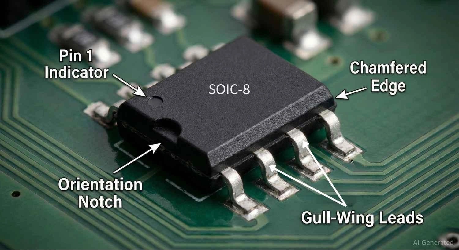
Technically defined, a SOIC package, short for Small Outline Integrated Circuit, is a surface-mount integrated circuit (IC) package characterized by two parallel rows of gull-wing leads. It offers a dramatic reduction in footprint.
Compared with equivalent DIP packages, SOIC typically reduces PCB area by roughly 30%–60%, depending on pin count and pitch.
The SOIC represents the "sweet spot" of assembly. SOIC is widely used because it balances density, manufacturability, and reworkability.
SOIC's gull-wing leads provide mechanical compliance and visible solder fillets, making it more tolerant to PCB warpage and rework than QFN in many production environments.
Small Outline Integrated Circuit (SOIC) Package Specifications
Understanding the precise physical attributes of the SOIC is critical for PCB layout and assembly. Unlike generic descriptions, a technical breakdown reveals the specific dimensions that dictate SMT stencil design and thermal performance.
| Package Type | Body Width (mm) | Pitch (mm) | Thermal Resistance ($\theta_{JA}$) |
|---|---|---|---|
| Narrow Body | 3.90mm (150 mil) | 1.27mm | ~100–120 °C/W |
| Wide Body | 7.50mm (300 mil) | 1.27mm | ~70–80 °C/W |
Note
$\theta_{JA}$ depends strongly on PCB copper and airflow, but typical SOIC $\theta_{JA}$ ranges from ~70 to 120 °C/W.
SOIC Package Dimensions and Body Variations
The SOIC package is primarily categorized by its body width. Designers must differentiate between these types to prevent solder mask-defined vs. non-solder mask-defined pad errors in CAD layouts.
-
Narrow Body SOIC
- Body Width: 3.90mm (approximately 150 mils)
- Typical Pin Counts: 8, 14, and 16 pins
- Usage: Standard logic gates, op-amps, and timers
-
Wide Body SOIC
- Body Width: 7.50mm (approximately 300 mils)
- Typical Pin Counts: 16, 20, 24, and 28 pins
- Usage: Interface ICs, larger microcontrollers, and memory chips requiring larger die attach pads
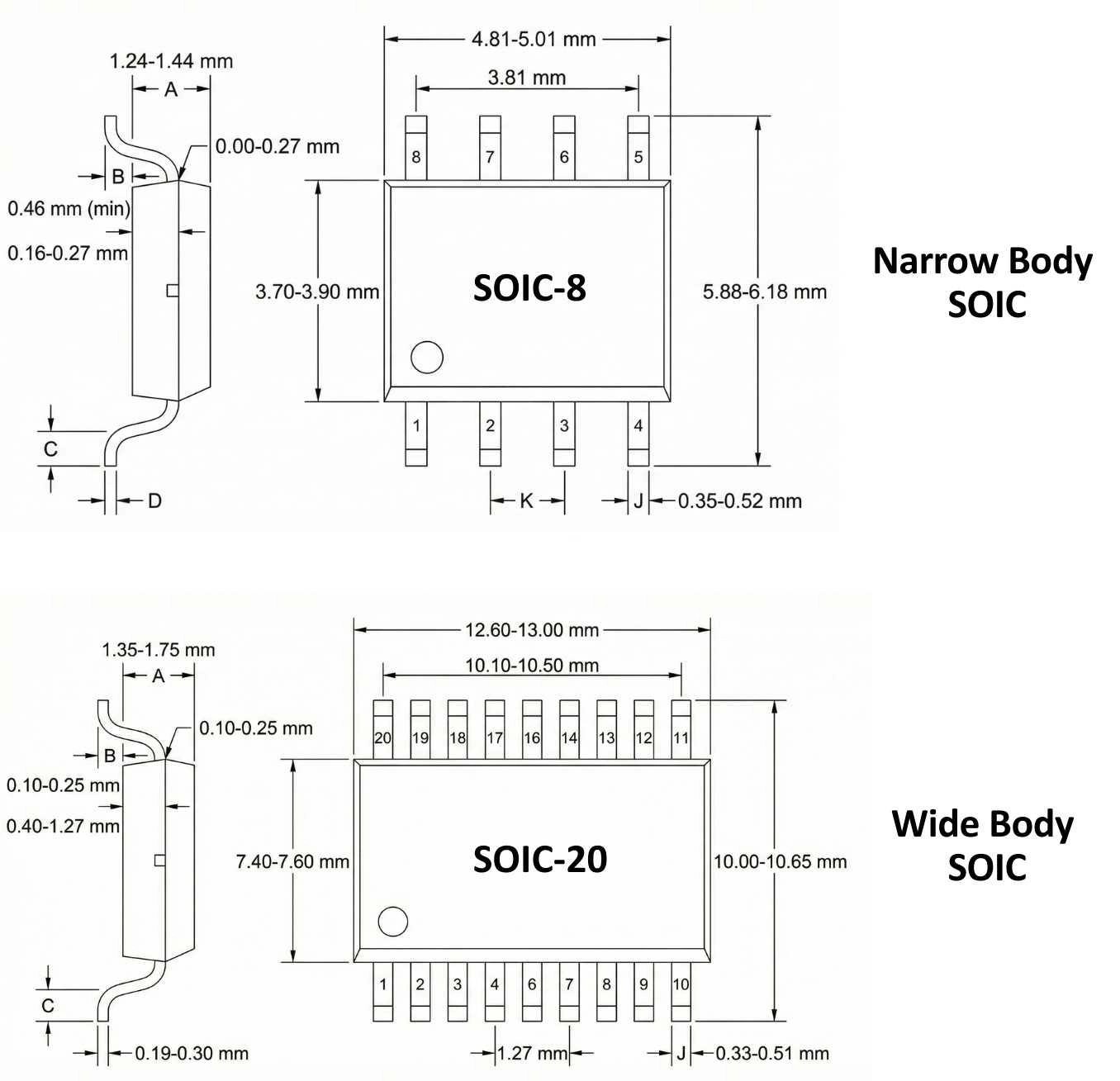
SOIC Package Lead Geometry, Pitch, and Coplanarity
The defining feature of the SOIC is its 1.27mm (50 mil) pin pitch. Unlike Fine-Pitch (FP) components such as the SSOP (0.65mm), the 1.27mm pitch allows for a wider process window during solder paste printing, significantly reducing the risk of solder bridging.
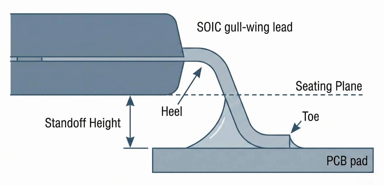
The Gull-Wing Mechanics: The leads of an SOIC are formed in a "gull-wing" configuration. Mechanically, this shape provides compliance. During operation, the silicon die, the plastic mold compound, and the FR-4 PCB substrate expand at different rates (CTE mismatch). The gull-wing leads act as flexible springs, absorbing this mechanical stress to protect the solder joints.
Gull-wing leads provide mechanical compliance that reduces stress transfer to solder joints during thermal cycling, improving reliability. It is a critical reliability factor for automotive and industrial PCBs.
Lead Coplanarity: For reliable SMT assembly, lead coplanarity — the vertical distance between the highest and lowest lead — must be maintained within 0.10mm (4 mils). Deviations outside this tolerance often result in "open" solder joints during the reflow process.
SOIC Package Materials, Leadframe, and Plating
- Leadframe: Leadframes are usually made from copper alloys (e.g., Alloy 42, 194, 172) depending on manufacturer and thermal requirements. Typically constructed from Copper Alloy 194 (CuFe2.3P) to maximize thermal conductivity (~260 W/m·K), facilitating heat transfer from the die to the PCB.
- Plating: Leads are plated with Matte Tin (Sn) or Nickel-Palladium-Gold (NiPdAu). This plating ensures wettability during the JLCPCB PCB assembly process and prevents oxidation during storage.
SOIC SMT Packaging and Handling Considerations
For automated assembly, SOIC components are supplied in Tape and Reel or Plastic Tubes.
- Tape and Reel: Preferred for high-volume SMT production. The components are placed in embossed pockets, carrier tape, sealed with a cover tape, allowing for rapid feeding into pick-and-place machines.
- Tubes: Common for smaller quantities or prototyping, but require stick feeders, which can be slower to load.
Common Applications of SOIC Package in Electronics
The Small Outline Integrated Circuit is versatile, finding its way into almost every sector of the electronics industry. Its balance of size and manual reworkability makes it particularly popular in scenarios where BGA is too complex to route or test, but DIP is too bulky.
| Industry Sector | Application Context | Why SOIC is Preferred | Common Examples |
|---|---|---|---|
| Medical Devices | Portable patient monitors, Pulse Oximeters | Reliable solder joints withstand drops/vibration; size fits handheld enclosures better than DIP. | Precision Op-Amps (e.g., OPA series), ADCs |
| Telecommunications | Routers, Modems, Base Stations | Excellent high-frequency performance due to short leads; standard footprint for transceivers. | RS-485 Transceivers (MAX485), Line Drivers |
| Development Boards | Arduino clones, ESP32 breakout boards, DIY Kits | Hand-solderable for hobbyists and students; easy to probe for debugging compared to QFN. | USB-to-UART bridges (CH340, CP2102), Regulators |
| Automotive | ECU (Engine Control Units), Dashboard Controllers | High tolerance for thermal cycling (gull-wing stress relief); AEC-Q100 qualified parts often utilize SOIC packaging. | CAN Bus Transceivers (TJA1050), Voltage Regulators |
| Wearable Tech | Smart watches (older generations), Health trackers | Used for power management where ultra-miniaturization (CSP) isn't strictly required but z-height matters. | Serial Flash Memory (SPI Flash), EEPROM |
| Industrial Automation | PLC Inputs, Motor Drivers | Robustness against factory vibration; ease of replacement/repair in the field. | Gate Drivers, Isolators, Solid State Relays |
SOIC Package vs Other IC Packages
Choosing the right package is a trade-off between electrical performance, thermal management, and assembly yield.
SOIC vs DIP (Dual In-line Package): Through-Hole vs SMT
While DIP is easier for breadboarding, it is electrically inferior. The long leads of a DIP package introduce significant parasitic inductance (L) and capacitance (C).
- Signal Integrity: The shorter leads of the SOIC minimize parasitic inductance, allowing for faster switching speeds and higher frequency operation (>100 MHz) with less signal degradation.
- Thermal Path: The SOIC sits flush against the PCB surface. Heat generated by the die has a shorter path to travel through the leads to the copper traces ($R_{\theta JL}$ is lower), improving thermal dissipation.
SOIC vs SOP (Small Outline Package): Understanding the JEDEC vs EIAJ Difference
A common technical pitfall is confusing the SOIC with the SOP (Small Outline Package), often defined by EIAJ/JEITA specifications.
- The Difference: EIAJ SOP packages typically have a body width of 5.3mm — wider than the Narrow SOIC (3.9mm) but narrower than the Wide SOIC (7.5mm).
- The Risk: Placing a standard SOIC footprint for an EIAJ SOP component often results in leads barely touching the pads, leading to weak or open joints.
- Solution: Always cross-reference the specific body width parameters in the datasheet when using the JLCPCB Parts Library.
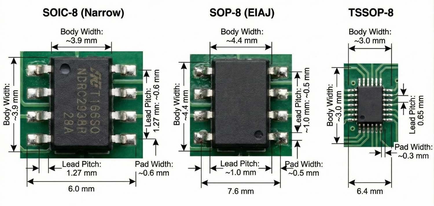
SOIC vs TSSOP and QFN: Size, Density, and Robustness
- TSSOP (Thin Shrink Small Outline Package): Features a thinner profile (1.1mm max) and tighter pitch (0.65mm). While space-saving, it is more susceptible to solder bridging and requires thinner stencils.
- QFN (Quad Flat No-lead): Offers superior thermal performance due to the direct thermal pad, but is difficult to prototype and inspect. SOIC allows for visual inspection of solder fillets without X-ray, simplifying Quality Control (QC).
SOIC PCB Footprint Design and DFM Guidelines
To ensure zero-defect manufacturing at JLCPCB, your PCB layout must adhere to strict Design for Manufacturing (DFM) guidelines. The physical land pattern determines the volume of solder paste deposited.
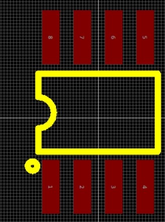
SOIC Land Pattern and Pad Design Requirements
The land pattern geometry dictates the formation of the solder joint.
- Toe Fillet (Outer): The pad must extend 0.35mm–0.55mm beyond the lead end. This allows a visible meniscus of solder, essential for Automated Optical Inspection (AOI) to verify the joint.
- Heel Fillet (Inner): The most critical joint for mechanical strength. The pad should extend inward sufficiently to allow solder to wet the "knee" of the lead.
- Solder Mask Dam: Ensure a solder mask web of at least 0.1mm (4 mils) exists between pads to prevent solder bridging, although the wide 1.27mm pitch makes this easily achievable.
Thermal Management for SOIC and SOIC-EP Packages
High-power ICs often use the SOIC-EP (Exposed Pad) variant, which includes a thermal slug on the bottom.
- Via-in-Pad Strategy: Place an array of 0.3mm thermal vias directly in the central ground pad. These should stitch to internal ground planes to dissipate heat.
- Stencil Aperture: Do not use a 100% aperture opening for the exposed pad. Use a "window pane" design (50–80% coverage) to prevent excessive solder lift, which can cause the package to float and disconnect the signal pins.
SOIC SMT Assembly Process and Common Defects
JLCPCB SMT Assembly service utilises precision pick-and-place machines, but understanding the process helps in designing robust boards.
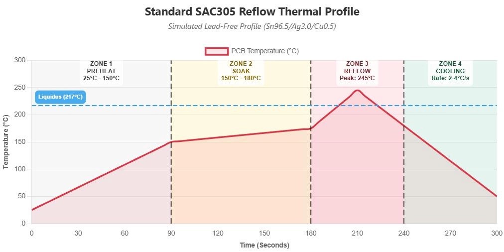
Reflow Soldering Profile for SOIC Package
-
Soak Zone (150°C–200°C)
60–120 seconds. Activates flux and ensures the plastic body and internal die reach thermal equilibrium to prevent warping.
-
Reflow Zone
Peak temperature: typically 235–245°C for SAC305, not exceeding the JEDEC maximum of 260°C.
-
Cooling
Rate of <4°C/s to ensure fine-grain solder structure without thermal shock.
SOIC Package Moisture Sensitivity Levels (MSL) and Storage
SOIC packages are hygroscopic. If moisture is trapped inside the plastic encapsulation during reflow, it expands into steam, causing "popcorning" (package cracking).
Protocol: High MSL components (Level 3+) are baked before assembly if exposure time is exceeded, following strictly controlled storage procedures.
SOIC Assembly Defects and Prevention Strategies
- Solder Bridging: Rare on 1.27mm pitch. If occurring, check if stencil thickness exceeds 0.15mm.
- Lead Lifting or Uneven Wetting: Ensure symmetric thermal relief connections on pads tied to large copper planes. Imbalanced heat flow during reflow can cause uneven wetting forces, resulting in lifted leads or insufficient fillet formation.
- AOI Verification: The gull-wing geometry allows top-down cameras to easily verify wetting angles, making SOIC one of the most reliable packages to inspect.
Conclusion: SOIC Package
The Small Outline Integrated Circuit (SOIC) remains a titan in the electronics industry. Its balanced physical characteristics make it the ideal choice for engineers who need higher density than DIP but require easier handling and better robustness than QFN or BGA packages. By understanding technical specifications and optimizing your PCB footprints, you ensure seamless manufacturing.
FAQ about SOIC Package
Q1. What is the typical thermal resistance ($\theta_{JA}$) of a standard SOIC-8 package?
A standard Narrow Body SOIC-8 typically has a Junction-to-Ambient thermal resistance ($\theta_{JA}$) of approximately 100°C/W to 120°C/W on a standard FR-4 board. This means for every Watt of power dissipated, the junction temperature rises by ~100°C. For power applications, use the SOIC-EP variant or ensure substantial copper pours on the PCB.
Q2. Can SOIC package withstand wave soldering?
Yes, standard SOIC packages can withstand wave soldering, provided they are glued to the bottom side of the PCB. However, due to the risk of solder bridging on the trailing leads, Reflow Soldering is the preferred method for modern SMT assembly at JLCPCB.
Q3. Why do some datasheets specify a "Power SOIC"?
A "Power SOIC" usually refers to the SOIC-EP (Exposed Pad) variant or a specific leadframe design where multiple pins are fused internally to the die paddle (often GND pins) to serve as heat sinks. These require specific PCB layout strategies for heat dissipation.
Q4. Can I hand-solder an SOIC package?
Absolutely. The 1.27mm pitch is considered "hand-solder friendly." It is spacious enough to use a fine-tip soldering iron without needing a microscope, making it ideal for prototyping before moving to mass production with JLCPCB SMT.
Q5. How does lead plating affect the shelf life of SOIC components?
SOIC leads plated with Matte Tin typically have a shelf life of 1–2 years before "tin whiskers," or oxidation becomes a concern. NiPdAu (Nickel-Palladium-Gold) plating offers a longer shelf life and better resistance to oxidation, which is crucial if you are stocking parts for long-term production.
Popular Articles
• SMD Diode Code Lookup: Full List, Marking Guide & Identification [2026 Guide]
• SMD Resistor Package Sizes: Complete Size Chart, Footprints & How to Choose
• SMD Capacitor Codes: Identification, Markings, and Polarity
• SMD Capacitor Sizes: Complete Size Chart and Selection Tips for PCB Design and Assembly
• How to Solder SMD Components Like a Pro [2026 Updated]
Keep Learning
PoP Package (Package on Package) Explained: Architecture, Assembly, and SMT Challenges
In the race for miniaturization, fitting more processing power into smaller footprints is the ultimate challenge for PCB designers. Package on Package (PoP) technology answers this by integrating logic and memory vertically, becoming the standard for modern mobile processors. However, this 3D architecture demands advanced SMT assembly capabilities beyond standard fabrication. JLCPCB specializes in the high-precision manufacturing required to master these complex stacks. This guide covers how PoP packa......
What Is a PQFP Package? Plastic Quad Flat Package Design, Footprint, and Assembly Guide
The Plastic Quad Flat Package (PQFP) is a widely used IC package in industrial, automotive, and embedded designs. This article provides a practical, engineering-focused guide to PQFP package. It explains how PQFP is built, when it makes sense to use it, how it compares with newer package types, and what designers should consider in terms of footprint design, thermal performance, signal integrity, manufacturing, and reliability. What Is a PQFP Package (Plastic Quad Flat Package)? A Plastic Quad Flat Pa......
Small Outline Integrated Circuit (SOIC): Package, Specs & Uses
As designs transition from legacy through-hole components to high-density Surface Mount Technology (SMT), the Small Outline Integrated Circuit (SOIC) remains the industry standard for operational amplifiers, flash memory, sensors, and microcontrollers. It stands as a testament to balanced engineering, offering a perfect compromise between the miniaturisation demanded by modern consumer electronics and the ruggedness required for industrial applications. This article serves as a definitive engineering ......
A Complete Guide to Surface Mount Device (SMD)
Imagine holding a smartphone in your hand. Inside that sleek device lies a complex network of thousands of miniature components — resistors smaller than a grain of rice, capacitors thinner than a fingernail, and integrated circuits containing millions of transistors. Without Surface Mount Technology (SMT) and its compact Surface Mount Devices (SMDs), none of this would exist. Just a few decades ago, electronics were bulky. Radios filled desks, computers filled rooms, and assembling a circuit meant dri......
Circuit Breaker Types Explained: MCB, MCCB, RCCB, RCBO, ACB, VCB & SF6 Circuit Breakers
A circuit breaker automatically disconnects power when it detects faults such as overloads or short circuits, protecting equipment and reducing fire risk. Different circuit breaker types are designed for different voltage levels, current ratings, and applications, from household distribution boards to high-voltage substations. This guide explains the most common types - including MCBs, MCCBs, RCCBs, RCBOs, ACBs, VCBs, and SF6 breakers and helps you choose the right one for your application. Figure: Ci......
Quad Flat Package (QFP): The Engineer's Guide to Design, Assembly and Thermal Management
What is QFP Package? The Quad Flat Package (QFP) is one of the most popular surface mount technology (SMT) package formats throughout the history of electronic manufacturing. After it became standard in the 1980s, the QFP has been the industry standard for integrated circuits (ICs) with moderate to high pin counts that typically range from 32 to 304 pins, so it was a good alternative for simple SOIC packages and complex Ball Grid Arrays (BGAs) at the same time. Defined by its "gull-wing" leads extendi......