How to Prevent Solder Bridges for Superior PCB Quality and Reliability
14 min
- What Solder Bridges Are and Why They Happen
- The Impact of Solder Bridges on PCB Performance and Reliability
- Design Strategies to Minimize Solder Bridge Risk
- Process Controls and Best Practices in Manufacturing
- Advanced Prevention Techniques and Alternative Solutions
- JLCPCB's Professional Approach to Solder Bridge Prevention
- FAQ about Solder Bridge
- Conclusion
Key Takeaways
- Solder bridges are a leading cause of SMT failures on fine-pitch components.
- Prevent them with proper solder mask dams (0.075–0.1mm), optimized stencil design, and controlled reflow profiles.
- Combine good DFM practices with AOI + X-ray inspection for maximum reliability.
- Professional manufacturing and early DFM review significantly boost first-pass yield and reduce costly rework.
You have experienced the post-reflow sadness and eyed the board that failed on the first reflow, if you have ever populated a fine pitch QFN or a 0.4mm BGA. After half a day of tracing around, I finally found it under the microscope: a small bridge of solder between two pads that should not have come into contact. It turned out that the little solder bridge was shorting a power rail to ground, and there was no firmware that could correct it. The worst thing is that solder bridges are not always visible as big blobs. Most of them are tucked between fine-pitch leads, under chip packages, or along the edge of a connector where you can't see them with the naked eye.

They get a great design and then make a paperweight of it without you knowing, and they do it at the last step of assembly after you've spent your time and money. I would like to go over the whole PCB solder bridge issue, as I've learned it on the bench and in production. What is a solder bridge, why does it form, and most importantly, the design and process controls to prevent their formation in the first place will be covered. Let's settle it.
What Solder Bridges Are and Why They Happen
Definition of Solder Bridge and Its Common Appearances
A solder bridge is a soldering artifact that unintentionally joins two adjacent pads, leads, or traces that were to remain electrically separate. It's basically a metal short circuit in the place of where you'd like to have an open gap. It may be a fat blob visible to the naked eye, or it may be a hair-thin filament that can only be seen under magnification or by X-ray. But where do these things like to hide?
The common denominator is proximity. The closer two solderable surfaces are together, the easier it will be for the molten solder to wick between them and remain there after it solidifies. That is why high-density and fine-pitch layouts require so much more discipline than a relaxed through-hole board ever did.
Primary Causes in SMT Assembly Processes
To understand what solder bridge formation is, you need to consider the entire SMT chain since the defect is rarely caused by a single factor. Usually, a short is caused by many small errors. The following are the root causes I always find myself returning to:
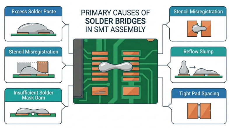
- Too much solder paste has been deposited due to the stencil aperture being too large or being overprinted.
- Chipping or mispositioning of the components during the pick-and-place process causes paste to be dragged between leads.
- Reflow profile issues: Too aggressive ramp, too long peak time, and Paste will slump and merge.
The Impact of Solder Bridges on PCB Performance and Reliability
Short Circuits, Functional Failures, and Field Returns
Solder bridge's immediate effect is a hard short. If a signal net is connected to a power rail or ground via a bridge, then the net will cease to behave and typically cause other nets to take a fall. If the short is across a power supply, then too much current can flow, and cause a regulator to overheat, and in extreme cases, cause damage to components that were fine prior to the short.
Some bridges do not, however, kill the board immediately, and this is what makes them dangerous. Some develop short circuits or intermittent contacts that pass a quick bench test and then fail weeks later in the field. A resistive bridge can alter bias points, cause high-speed signals to become corrupted, or cause a device to reset under load. Those are the units that become field returns, and field returns are much more expensive than a defect found at the factory. A board at AOI is a board that you lose, a board that fails in a customer product is a board, shipping, diagnosis, and a loss of trust.
Cost and Reputation Consequences for Manufacturers
When it comes to defects, there is no two ways about it. It's all a numbers game, and solder bridges are on the wrong side of the equation! It is often said that the cost of every bridge that escapes inspection is multiplied as it travels downstream (rule of ten): $1 to fix it at assembly, $10 to fix it at test, $100 to fix it in the field. In addition to the cost, there is a loss of first-pass yield, or the percentage of boards that pass without rework, due to repeated bridging. Low 1st pass yield causes high labor, slow delivery, and an unpredictable whole line. That reputation blow can be as significant to a contract manufacturer as the scrap itself.
Design Strategies to Minimize Solder Bridge Risk
Pad Design, Solder Mask Expansion, and Component Spacing Rules
The ideal location to kill a solder bridge is in your layout, well before you print any paste. Good pad geometry provides a molten solder with a definite home to rest, and good spacing prevents it from roaming. There are two options to choose from: solder mask defined (SMD) pads or non-solder-mask defined (NSMD) pads. NSMD pads use a smaller copper than the mask opening to provide a more consistent joint for BGAs, but it introduces a problem: exposed copper that can be a problem if spacing is tight. SMD pads, which are where the mask overlaps the copper edge, provide a built-in dam that helps contain solder and therefore are often preferred in tight, fine pitch fields. Some of my mantras to rely on at all times:
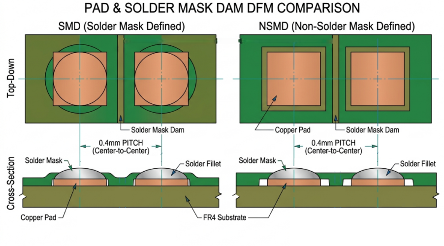
- Keep a solder mask dam between two adjacent pads; the dam size is 0.075mm to 0.1mm. This is the one dam that can make or break a bridge for 0.4mm and 0.5mm pitch parts.
- Set solder mask expansion to ensure that openings do not become so large that adjacent pads become one large window.
- Use component spacing courtyards as per IPC-7351 land pattern guidelines, and do not place the parts as close together as the silkscreen permits.
DFM Guidelines for High-Density and Fine-Pitch Layouts
With high-density designs, your DFM (Design for Manufacturing) discipline must “go to the races” with the pitch. The closer the pitch, the closer the short is to being a clean joint. Here are some practical DFM habits that will pay off:
- Use IPC-7351 footprints to match pad size to the package; avoid hand-rolling pads that are too long to avoid slumping.
- Placing routing in dense areas, stagger or fan out to prevent awkward placement of copper features near solderable areas.
- Ask for the minimum solder mask sliver width that your fab can print; don't assume.
- Include fiducials close to fine pitch components to ensure pick and place and stencil alignment does not become compromised.
Process Controls and Best Practices in Manufacturing
Stencil Design, Solder Paste Volume, and Reflow Profile Optimization
Now that the design is good, once the board is assembled, the bridges are prevented or directly printed on the board. It begins with the stencil, as the stencil determines where the paste goes. The important number here is the area ratio, which is the ratio of the area of an aperture opening to the area of its wall.
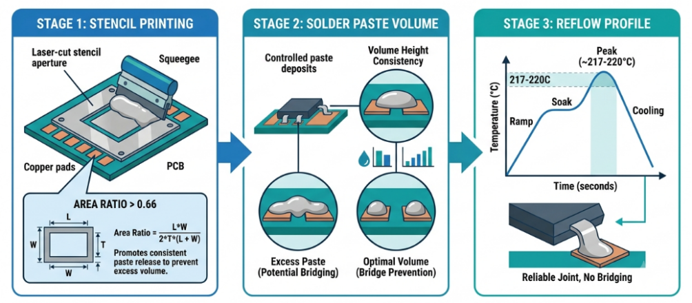
As a rule of thumb, you want to have an area ratio greater than 0.66 for reliable paste release; otherwise, the paste may clog the aperture or transfer inconsistently, which will lead to bridging. When making fine pitch parts, I will often decrease apertures as compared to the pad size, sometimes using a home plate or an inset shape to reduce paste volume right at the bridge area. Reflow is the next step after printing, and the profile is as important as the paste. A controlled ramp, stable soak, and a well-bounded peak prevent the solder from slumping or merging.
Inspection Methods Including AOI and X-Ray for Early Detection
Inspection is the safety net to catch the bridges your process still lets through, since you can't fix what you can't see. AOI and X-ray are the two workhorses and have different blind spots. AOI (Automated Optical Inspection) is a process that utilizes cameras and lighting for checking the board surface for bridges, missing parts, and polarity errors.

It's in-line, fast, and is excellent at picking up exposed leads with visible bridges. What it can't do is see under a package. This is where X-ray inspection comes in handy. X-RAY inspection will show the bridges and voids that optical systems just can't get to for BGAs, QFNs, and any joint that is not accessible under the body of the part. Combining the two, AOI for surface defects and X-ray for the hidden defects, provides coverage to capture a solder bridge before it ever gets out into the field on the line.
Advanced Prevention Techniques and Alternative Solutions
No-Clean vs Clean Flux Selection and Cleaning Processes
Although less ostentatious than stencils or reflow, flux chemistry is nonetheless important when it comes to bridging; it affects reliability after assembly. There are two general categories: no-clean fluxes and water-soluble (clean) fluxes, each of which has its advantages and disadvantages.
- No-clean flux leaves a small residue (that is not harmful) that is intended to remain on the board, making the process easier and not requiring a wash step. Here is the rub: The residue can obscure marginal bridges for inspection and, when the chemistry is not right for the board, leave residue that counts on high-impedance nets.
- Water-soluble flux is more aggressive and can be removed completely, leaving the board clean, but it requires a good wash down, as the flux that remains is corrosive.
When a design contains fine pitch parts with sensitive analog or high voltage nets, it is essential that a proper cleaning process is used to remove any residues that might mask or even promote leakage paths between closely spaced pads.
When to Consider Alternative Surface Finishes or Assembly Methods
Sometimes the best solution is to alter the finish or assembly method instead of repeatedly battling the same bridge. The surface finish will impact the ability of solder to wet and spread, which in turn directly impacts bridging on tight geometries. Some situations in which it may be helpful to reconsider the strategy:
- For fine pitch and BGA applications, opt for a flat finish, such as ENIG, over HASL to make fine pitch printing more consistent, as HASL's uneven solder bumps make it more difficult to print.
- For parts that require coplanarity at a pitch of less than 0.4mm, consider OSP or immersion finishes.
- If a joint is hidden and is likely to be re-worked, consider using a different package or a selective soldering operation involving nearby through-hole parts to reduce the overall bridge risk.
JLCPCB's Professional Approach to Solder Bridge Prevention
Rigorous DFM Review Focused on Solderability Risks

One thing I like about the manufacturer JLCPCB is that bridge prevention begins before the board is even created. Their engineering DFM review catches solderability issues early, such as pad spacing, solder mask slivers, and aperture issues with fine pitch footprints, and catches these problems while they're still a “quick edit” and not a “scrap report.” This is the discipline we spoke about in the design section, and it applies automatically to your files. It is the gap between wishful thinking that your layout can be manufactured and knowing that it was verified against actual process limits.
High First-Pass Yield Through Advanced Quality Systems
The payoff is at inspection. When combined with X-ray checking of hidden joints (BGA and QFN) and surface joints, AOI scanning ensures escaped bridges are caught before boards are shipped, resulting in high first pass yield and low field return rates. To anyone transitioning from a few prototypes to a production run, that mix of DFM, SMT control, and layered inspection makes the solder bridge a non-existent problem. It is the actual realization of all the above, a prototype-friendly price.
FAQ about Solder Bridge
Q: What exactly is a solder bridge on a PCB?
A solder bridge is an unintended bead or filament of solder that connects two adjacent pads, leads, or traces meant to stay separate. It creates a short circuit, which can cause anything from a dead net to an intermittent field failure, depending on where it sits.
Q: What are the most common causes of solder bridges?
The usual causes are excess solder paste, an oversized or misregistered stencil aperture, an insufficient solder mask dam between fine-pitch pads, component skew, and reflow profile problems that let paste slump. Most real-world bridges come from several of these factors stacking up together.
Q: How do I fix a solder bridge once it has formed?
Apply fresh flux over the bridge, then use solder wick with a fine-tipped iron to draw away the excess solder. Inspect the gap under magnification, add a little fresh solder if the joint looks starved, and clean off the residue to confirm the short is gone.
Q: Why is solder mask important between fine-pitch pads?
The thin strip of solder mask between pads, called a solder mask dam, physically blocks molten solder from flowing across the gap during reflow. On 0.4mm and 0.5mm pitch parts, this dam is often the single most effective barrier against bridging.
Q:Can AOI catch every solder bridge?
No. AOI excels at finding bridges on exposed leads and visible joints, but it cannot see underneath packages like BGAs and QFNs. Those hidden bridges require X-ray inspection, which is why high-reliability lines pair the two methods together.
Conclusion
A solder bridge is a little problem that can be very big and destroy a good board, and it resides at the cross-disciplinary point of design, stencil, paste, and reflow. There is no single setting that prevents it, but rather it's a stack of the odds in your favor by disciplined pad and mask geometry. A stencil optimized for the appropriate area ratio and a strict reflow profile, plus two-step inspection. The good news is that each and every one of these controls is well understood and fully repeatable. Once you think of solderability as a design input starting at the first footprint, and use DFM review along with AOI and X-ray, bridges cease to become a mystery to be chased down the microscope. When you want to implement these principles, it is easy to obtain clean, bridge-free boards from prototype to production with JLCPCB's DFM check, fabrication, and precision SMT assembly service.
Keep Learning
How Copper Foil Shapes PCB Performance and Manufacturing Quality
Key Takeaways Weight: 1 oz copper ≈ 35 µm thickness; higher weight increases current capacity. Types: ED for standard rigid boards, RA for dynamic flex circuits. DFM & Loss: Smoother foil lowers RF loss; thicker foil requires wider trace spacing. The part of a PCB that actually carries the electrical signal is the copper foil. The strength comes from the glass weave, the resin is used to keep the layers together, and the solder mask is used to provide protection and separation of exposed copper. But w......
A Complete Guide to Copper Clad Laminate (CCL) in PCB Manufacturing
Key Takeaways CCL is the base material: a cured resin-reinforcement sheet with copper foil bonded to one or both sides. Three parts control performance: Resin affects heat and loss, reinforcement controls stability, and copper foil affects conductor behavior. Choose by the main design stress: Heat, frequency, and cost usually determine the best laminate family. Slash sheets define the material: IPC-4101 uses numbered slash sheets to specify rigid PCB base materials. Tg alone is not enough: Td and time......
Buried Vias in Advanced PCBs: Enabling Higher Density, Better Signal Integrity, and Compact Designs
Key Takeaways Hidden Routing: Buried vias connect only inner layers, keeping outer surfaces clear for dense components and traces. Better Signal Integrity: They eliminate via stubs, reducing parasitics and signal loss in high-speed designs. Higher Density: Essential for HDI boards, dense BGAs, and small form factors like wearables. Higher Cost: Sequential lamination and extra drilling steps make them ~3×-4× more expensive than standard through-holes. Ever wondered how a modern smartphone mainboard can......
Unlocking Higher Density and Better Performance with Blind Vias in HDI PCBs
Key Takeaway Higher Density: Connects surface to inner layers without penetrating the whole board, freeing routing channels under fine-pitch BGAs. Improved Signal Integrity: Reduces via stub length to minimize impedance discontinuities in high-speed designs. Aspect Ratio Rule: Keep the depth-to-diameter ratio near 0.75:1 (max 1:1) for reliable laser drilling and void-free plating. Thermal Efficiency: Supports via-in-pad setups for better heat dissipation and compact component placement. Ever wonder ho......
How to Select Tg of PCB ?
What is the Tg of PCB? In PCB manufacturing, "Tg" stands for Glass Transition Temperature. It is the temperature at which the PCB substrate material transitions from a rigid, glassy state to a soft, rubbery state. PCBs are flame-retardant (UL94 V-0) and do not burn easily; instead, they soften above Tg. The Critical Correlation Between Tg and Z-Axis CTE (Coefficient of Thermal Expansion) When the temperature exceeds the Tg point, the PCB substrate material (such as standard FR-4) undergoes a physical ......
Beyond the Basics: The Role of PTFE PCBs
Polytetrafluoroethylene (PTFE) PCBs are integral to advanced electronic applications. Among various PCB materials, Teflon, the brand name for Polytetrafluoroethylene (PTFE). Teflon PCBs, known for their high frequency and heat resistance properties. All of this is achievable due to its exceptional dielectric properties. RF PCB designs often make use of low-loss PTFE-based materials thanks to their very low dielectric losses and huge range of possible Dk values. Low Dielectric Constant: Enables high-sp......