
The Ultimate Guide to Wafer Level Packaging (WLP): Process, Types, Benefits, and Applications
17 min
- What Is Wafer Level Packaging (WLP)?
- Wafer Level Packaging: Electrical Performance Characteristics
- Wafer Level Packaging vs Traditional Packaging: Key Differences
- Wafer Level Packaging Process Flow
- Types of Wafer Level Packaging
- Materials and Technologies Used in Wafer Level Packaging
- Key Benefits of Wafer Level Packaging
- Challenges and Limitations of Wafer Level Packaging
- Cost Analysis: Is Wafer Level Packaging More Affordable?
- Reliability and Testing in Wafer Level Packaging
- Applications of Wafer Level Packaging
- Real-World Use Cases of Wafer Level Packaging
- Wafer Level Packaging vs Other Advanced Packaging
- From Wafer-Level Packaging to PCB Assembly: Bridging Chip Design and Manufacturing
- Design Considerations for Engineers Using Wafer Level Packaging
- PCB Design Rules for Wafer-Level Packages (WLP)
- Future Trends in Wafer Level Packaging
- FAQ about Wafer Level Packaging
- Conclusion
Modern electronics are hitting a hard limit: you can’t keep shrinking devices without rethinking how chips are packaged. As PCB space tightens and signal speeds increase, traditional packaging methods introduce too much size, parasitic loss, and inefficiency.
Wafer-level packaging (WLP) addresses this by forming interconnects directly on the wafer before singulation, eliminating substrates and shortening signal paths. The result is a chip-scale package with higher integration density, lower parasitics, and better high-frequency performance, widely used in smartphones, IoT, and automotive systems.
In this guide, you'll learn the WLP process flow, key types (fan-in, fan-out, WLCSP), benefits and limitations, real-world engineering use cases, and practical PCB design considerations.
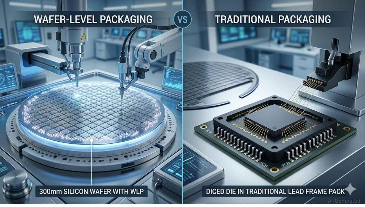
Figure: Wafer-level packaging performed before dicing vs traditional packaging after dicing
What Is Wafer Level Packaging (WLP)?
Wafer-level packaging (WLP) is a semiconductor packaging process where integrated circuits are packaged at the wafer stage before dicing, enabling a smaller size, better performance, and lower cost.
Unlike traditional methods that cut the wafer first and package individual dies later, a wlp package eliminates traditional encapsulation and streamlines the manufacturing process. This direct approach birthed the wafer-level chip-scale package (WLCSP), meaning the final package is virtually identical in size to the bare die itself.
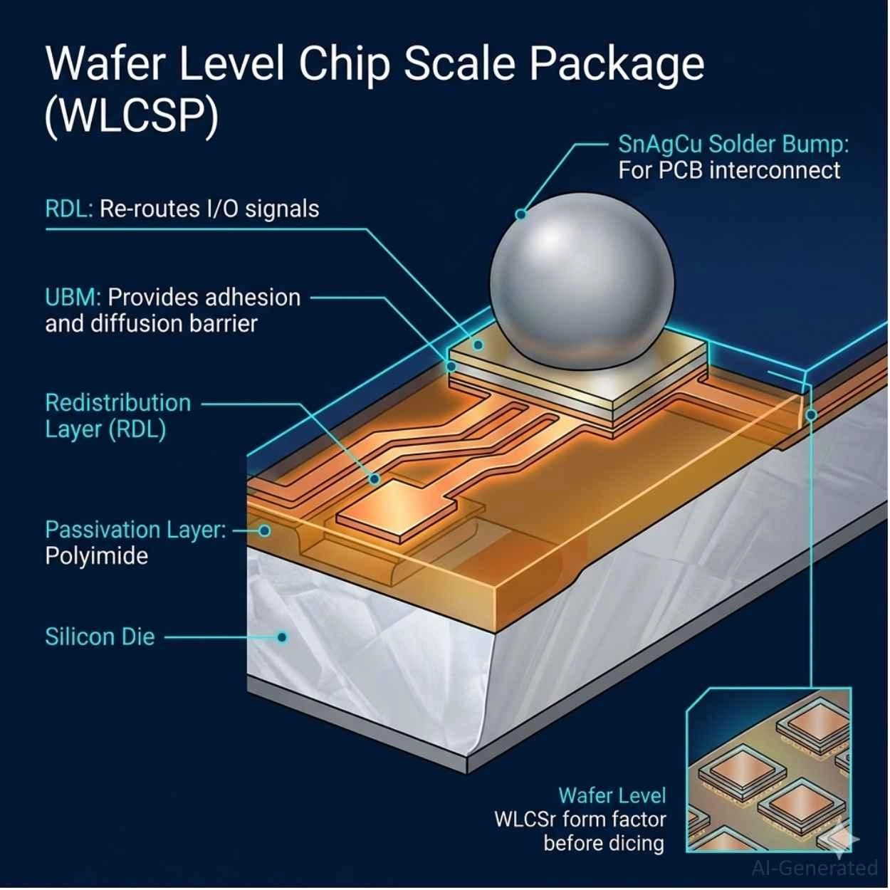
Figure: Cross-section of WLP showing RDL, UBM, and solder bumps
Wafer Level Packaging: Electrical Performance Characteristics
Beyond mere size reduction, the true power of WLP lies in its electrical behavior. Because the die connects directly to the PCB without intermediate wire bonds or thick substrates, it possesses unique WLP electrical performance traits, including:
- Lower parasitic inductance (L): improves high-frequency behavior
- Lower resistance (R): reduces conduction loss
- Reduced loop area: minimizes EMI and ringing
Shorter interconnects reduce loop inductance, improving impedance control and minimizing signal ringing. This makes WLP absolutely indispensable for high-frequency RF front-ends, 5G millimeter-wave components, and high-speed digital transceivers.
Wafer Level Packaging vs Traditional Packaging: Key Differences
When comparing wafer-level packaging vs traditional packaging, the most profound difference lies in the order of operations. Traditional packaging relies on wire bonding or lead frames, drastically increasing the volumetric footprint.
By contrast, WLP eliminates these intermediate structures, reducing interconnect length by ~30–60% vs wire bonding, which translates directly to faster signal propagation.
| Process Stage | Package Size | Electrical Performance | Cost | Yield Sensitivity | Thermal Performance | Assembly Complexity |
|---|---|---|---|---|---|---|
| Wafer Level Packaging | Equals die size (WLCSP) | Excellent (low inductance) | Low at high volumes | Highly sensitive | Shorter thermal path | High (precision SMT) |
| Traditional Packaging | Much larger than die | Moderate (wire bond parasitics) | Low at low volumes | Less sensitive | Insulating plastic mold | Low (standard SMT) |
Wafer Level Packaging Process Flow
The wafer-level packaging process flow is a sophisticated sequence of photolithography, deposition, and etching. Let's break down the critical steps.
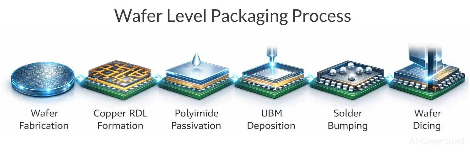
Figure: Step-by-step wafer-level packaging process flow from bumping to dicing
Wafer Fabrication (FEOL/BEOL Context)
This is the foundational step where the active transistors (FEOL) and internal metal routing (BEOL) are completed on the blank silicon wafer.
Redistribution Layer (RDL) Formation
The redistribution layer (RDL) reroutes the peripheral I/O pads of the die to an area array. This involves precise photolithographic masking and copper electroplating to create microscopic conductive traces. Advanced RDL processes use semi-additive copper plating with sub-5 µm line/space resolution, requiring tight lithography alignment tolerances.
Passivation and Protection
To protect the delicate copper traces, a polyimide dielectric layer is spun onto the wafer. This provides necessary electrical isolation and buffers mechanical stress. Polyimide thickness and curing conditions directly influence stress distribution and long-term reliability.
Under-Bump Metallurgy (UBM)
Before solder can be applied, UBM layers are deposited-often via sputtering vs electroplating. These adhesion and barrier layers prevent the solder from diffusing into the copper RDL. Improper UBM design can lead to intermetallic growth and premature solder joint failure.
Solder Bumping
Next, solder alloys, typically SnAgCu (SAC) micro-bumps, are deposited onto the UBM. These form the physical and electrical connections for the final PCB assembly. Bumping can be performed using electroplating or stencil printing, depending on pitch and volume requirements.
Wafer Thinning
Back grinding is performed to reduce the overall Z-height of the wafer. Wafer thinning is a critical step for ultra-thin mobile electronics. Excessive thinning increases wafer fragility and handling risk during downstream processing.
Wafer Dicing
In the final stage, the wafer undergoes singulation to produce individual chip-scale packages. Any RDL defects introduced prior to this phase directly compromise total yield, anchoring the absolute necessity for high-grade cleanroom environments to maintain strict manufacturing reality. Mechanical or laser dicing must minimize edge chipping, which can propagate cracks into active die regions.
Types of Wafer Level Packaging
As device complexity scales, different geometries have evolved to handle varying input/output (I/O) densities.
Fan-In Wafer Level Packaging (FI-WLP / Fan-In WLCSP)
In fan-in wafer-level packaging, all RDL traces and solder bumps are constrained entirely within the footprint of the silicon die. Because the bumps cannot exceed the die's area, the fan in WLCSP is typically restricted to chips with limited I/O requirements.
Wafer-Level Chip Scale Package (WLCSP)
The standard WLCSP package is the purest form of fan-in technology. Its size equals the die, making it the dominant choice for mobile IC usage and power management chips.
Fan-Out Wafer Level Packaging (FO-WLP / FOWLP)
When a chip requires more connections than its surface area allows, engineers turn to fan-out wafer-level packaging (FOWLP). Here, singulated dies are embedded in an artificial epoxy molding compound. The RDL extends beyond the original die into this molded area, allowing for a much larger bump array. Industry giants like TSMC and ASE Group have pioneered high-density FOWLP to support modern smartphone processors.
3D Wafer Level Packaging
3D wafer level packaging stacks multiple active silicon dies vertically using Through-Silicon Vias (TSVs). This technology drastically shortens memory-to-processor distances for extreme bandwidth.
Wafer Level Packaging Comparison
| Type | I/O Count | Use Case | Limitation |
|---|---|---|---|
| Fan-In (WLCSP) | <200 | Mobile ICs | Limited I/O |
| Fan-Out (FOWLP) | 200–1000+ | High-density SoCs | Complex process |
| 3D WLP | 1000+ | HPC/AI | High cost |
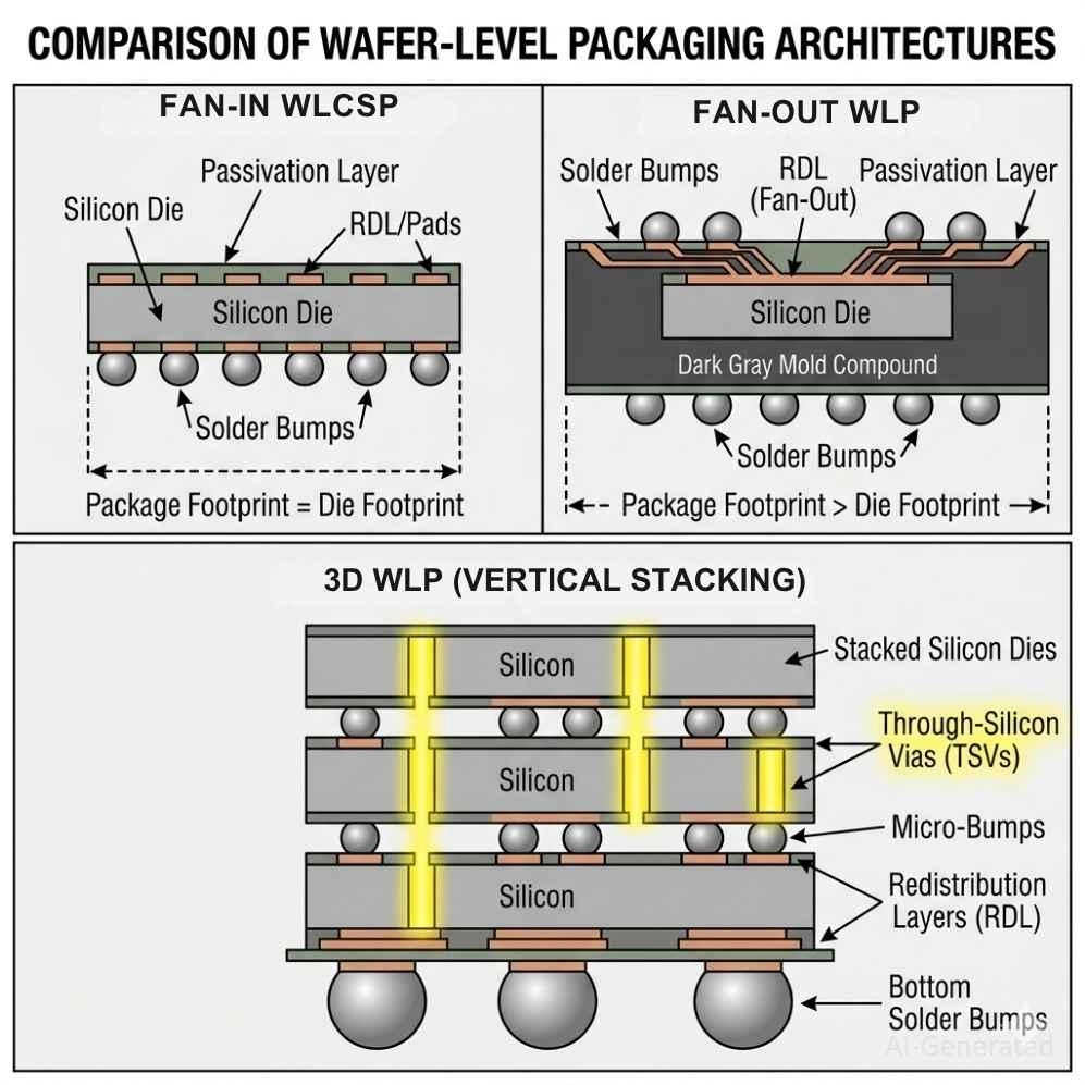
Figure: Difference between Fan-In, Fan-Out, and 3D Wafer Level Packaging architectures
Materials and Technologies Used in Wafer Level Packaging
The reliability of WLP relies entirely on the precise selection of wafer-level packaging materials.
A primary material is photosensitive polyimide, used for passivation due to its ideal dielectric constant (~3.0–3.5) and thermal stability. For the conductive pathways, RDL copper is utilized with typical thicknesses ranging from 5 to 20 µm.
The UBM layers typically consist of a robust multi-metal stack, such as TiW/Cu/Ni/Au (Titanium-Tungsten barrier, Copper seed, Nickel barrier, Gold oxidation protection). A critical engineering constraint here is managing the Coefficient of Thermal Expansion (CTE) mismatch between the silicon die, the solder alloys, and the final PCB.
Key Benefits of Wafer Level Packaging
The core wafer-level packaging advantages directly address the most pressing constraints in modern hardware design.
| Benefit | Technical Cause | Impact |
|---|---|---|
| Extreme Miniaturization | Elimination of traditional lead frames and wire bonds | Up to a 40% volume reduction compared to standard BGAs. |
| Superior Signal Integrity | Reduced parasitic inductance (L) from direct bumping | Cleaner high-frequency RF transmission and faster signal rise times. |
| Cost Efficiency at Scale | Parallel processing of thousands of chips on a 300mm wafer | Tangibly lower per-unit cost for mass-market, high-volume production. |
Challenges and Limitations of Wafer Level Packaging
- Warpage (CTE mismatch): Driven by severe thermal expansion differences (e.g., Silicon at ~2.6 ppm/°C vs. standard PCB FR4 at ~15 ppm/°C).
- Corner solder fatigue: Solder joints experience the highest mechanical strain due to their maximum distance from the neutral point (DNP).
- Yield sensitivity: Because the package acts directly as the interconnect, if a single solder bump fails during placement, the entire device is typically rejected.
When NOT to Use Wafer Level Packaging
A crucial part of engineering design is knowing the trade-offs. WLP is generally not recommended for:
- High-power applications: limited thermal dissipation
- Large dies: increased DNP stress
- Low-volume production: poor cost efficiency
Cost Analysis: Is Wafer Level Packaging More Affordable?
Evaluating wafer-level packaging cost requires separating initial CapEx from volume unit pricing. The machinery required for advanced RDL lithography and wafer bumping is capital-intensive.
A standard WLP cost breakdown includes:
- Mask Cost (NRE): Extremely high upfront cost for precision photolithography masks.
- RDL Cost: Increases linearly with layer count and tighter line/space resolution requirements.
- Yield Loss Impact: Packaging defects directly reduce the final output of usable Known Good Dies (KGD).
However, because packaging happens simultaneously across an entire wafer, this economy of scale typically crosses the cost-efficiency threshold against standard BGAs at production volumes exceeding 1 to 2 million units (depending on process node), making WLP drastically cheaper for mass-market hardware.
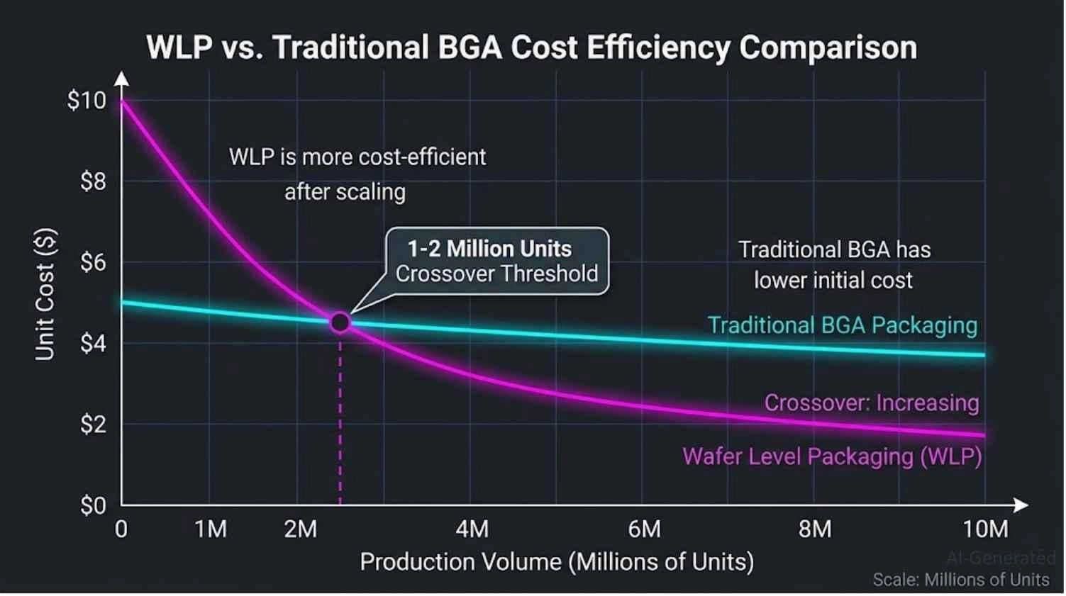
Figure: Graph showing WLP cost efficiency improving as production volume scales
Reliability and Testing in Wafer Level Packaging
Guaranteeing WLP reliability requires rigorous mechanical and thermal verification before chips hit the market. Foundries test these components using strict JEDEC testing standards. Common evaluations include:
- Thermal cycling: Rapidly shifting from -40°C to +125°C to induce and measure CTE-related stress fractures on critical corner balls.
- Drop testing: Mechanical evaluations to ensure the delicate micro-bumps survive drops in consumer environments.
- Moisture Sensitivity Level (MSL): Testing to guarantee the internal polymer layers do not absorb ambient humidity before the reflow process.
Applications of Wafer Level Packaging
Wafer-level packaging is widely used where miniaturization, high-frequency performance, and integration density are critical.
Smartphones and Wearables
Why WLP: ultra-small footprint, low parasitics, thin profile
Impact: dense PCB layouts, efficient power delivery, improved RF performance
Used in PMICs, RF front-end modules, and sensor interfaces.
MEMS Sensors
Why WLP: wafer-level (often quasi-hermetic) sealing, batch packaging
Impact: consistent cavity conditions, better sensor accuracy, lower cost
Common in accelerometers and gyroscopes.
Automotive Electronics
Why WLP: compact size, high-frequency signal integrity
Impact: improved radar performance, reduced module size
Note: requires underfill and strong PCB design for reliability
IoT Devices
Why WLP: minimal footprint, low parasitic loss, cost efficiency
Impact: enables compact, low-power wireless modules and sensor nodes
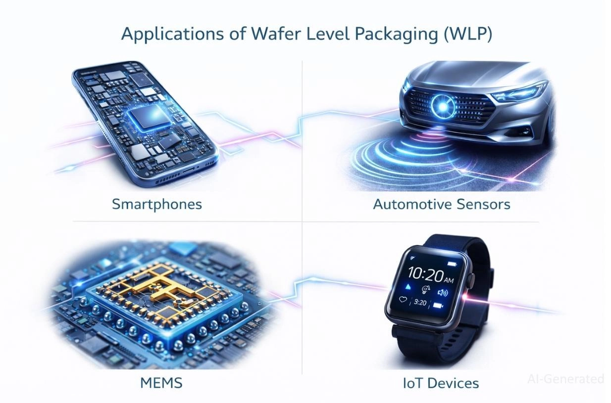
Figure: Applications of WLP across smartphones, automotive sensors, IoT devices, and MEMS
Real-World Use Cases of Wafer Level Packaging
In real hardware design, wafer-level packaging is selected not by application category, but by specific electrical, mechanical, and manufacturing constraints.
Ultra-Fine Pitch PCB Integration (WLCSP)
In compact designs, engineers often face routing limitations when dealing with sub-0.4 mm pitch devices.
Problem: Limited PCB routing channels under dense I/O arrays
WLP Role: Direct die-scale package minimizes footprint but forces HDI routing
Engineering Impact:
- Requires microvias and via-in-pad structures
- Increases PCB layer count and fabrication complexity
- Demands tight solder mask and stencil control
Used extensively in compact mobile designs by companies like Apple Inc. for PMICs and RF modules.
Power Delivery Network (PDN) and RF Optimization
Modern chips require stable, low-impedance power delivery at high switching speeds.
Problem: Voltage droop and noise due to parasitic inductance
WLP Role: Short interconnect path reduces inductive loop
Engineering Impact:
- Improved transient response
- Lower IR drop
- Better decoupling effectiveness near die
Widely adopted in mobile SoC ecosystems by Qualcomm, especially in 5G RF front-end modules.
Board-Level Reliability (BLR) Challenges
In real deployments, mechanical stress becomes a dominant failure factor.
Problem: CTE mismatch between silicon and PCB causes stress during thermal cycling
WLP Role: Direct solder connection increases sensitivity to stress
Engineering Impact:
- Corner ball fatigue (high DNP effect)
- Need for underfill in harsh environments
- Strict PCB material selection required
WLP improves performance but tightens reliability margins.
Heterogeneous Integration Without Substrates (FOWLP)
Advanced designs increasingly integrate multiple dies into a single package.
Problem: Traditional substrates add thickness, cost, and parasitics
WLP Role: Fan-out enables redistribution without organic substrate
Engineering Impact:
- Thinner packages
- Higher interconnect density
- Enables chiplet-style integration
Used in advanced packaging flows from companies like TSMC.
Wafer Level Packaging vs Other Advanced Packaging
| Feature | WLP | BGA | Flip Chip | SiP |
|---|---|---|---|---|
| Package Size | Smallest (≈ die size) | Medium | Medium | Varies |
| I/O Capability | Low–Medium | Medium | High | Very High |
| PCB Routing Difficulty | Very High | Low | Medium | High |
| Thermal Performance | Limited (PCB dependent) | Good | Very Good | Depends on design |
| Cost Efficiency | High at volume | Moderate | High cost | High cost |
| Integration Level | Low | Low | Medium | High |
WLP vs BGA
When looking at various BGA package types, Ball Grid Arrays (BGAs) utilize a laminate substrate to fan out I/O to a much wider pitch (typically 0.8–1.2 mm). While this relaxes PCB routing constraints and reduces the need for complex micro-vias, it significantly increases the volumetric footprint and introduces parasitic inductance through the substrate traces, unlike the ultra-low-profile, direct-attach nature of WLP.
WLP vs Flip Chip
Comparing wafer-level packaging vs flip chip (FCBGA) reveals fundamental structural differences. While both employ micro-solder bumps, flip chips mount the die onto an organic intermediate interposer or substrate, which is then attached to the PCB. WLP eliminates this substrate entirely, mounting the bare die directly to the main PCB.
This absence of a substrate in WLP drastically shortens the signal path for superior high-frequency performance, but it also demands strict board-level underfill to mitigate the extreme CTE mismatch between the silicon and the FR4 board.
WLP vs System-in-Package (SiP)
A System-in-Package (SiP) integrates multiple distinct active and passive components, such as logic, memory, and RF front-ends-into a single molded module utilizing a complex internal substrate. Conversely, a standard WLCSP is typically restricted to the packaging of a single monolithic die.
While advanced Fan-Out WLP (FOWLP) is blurring these lines through heterogeneous chiplet integration, SiPs currently offer a more mature and thermally forgiving ecosystem for mixing disparate silicon nodes.
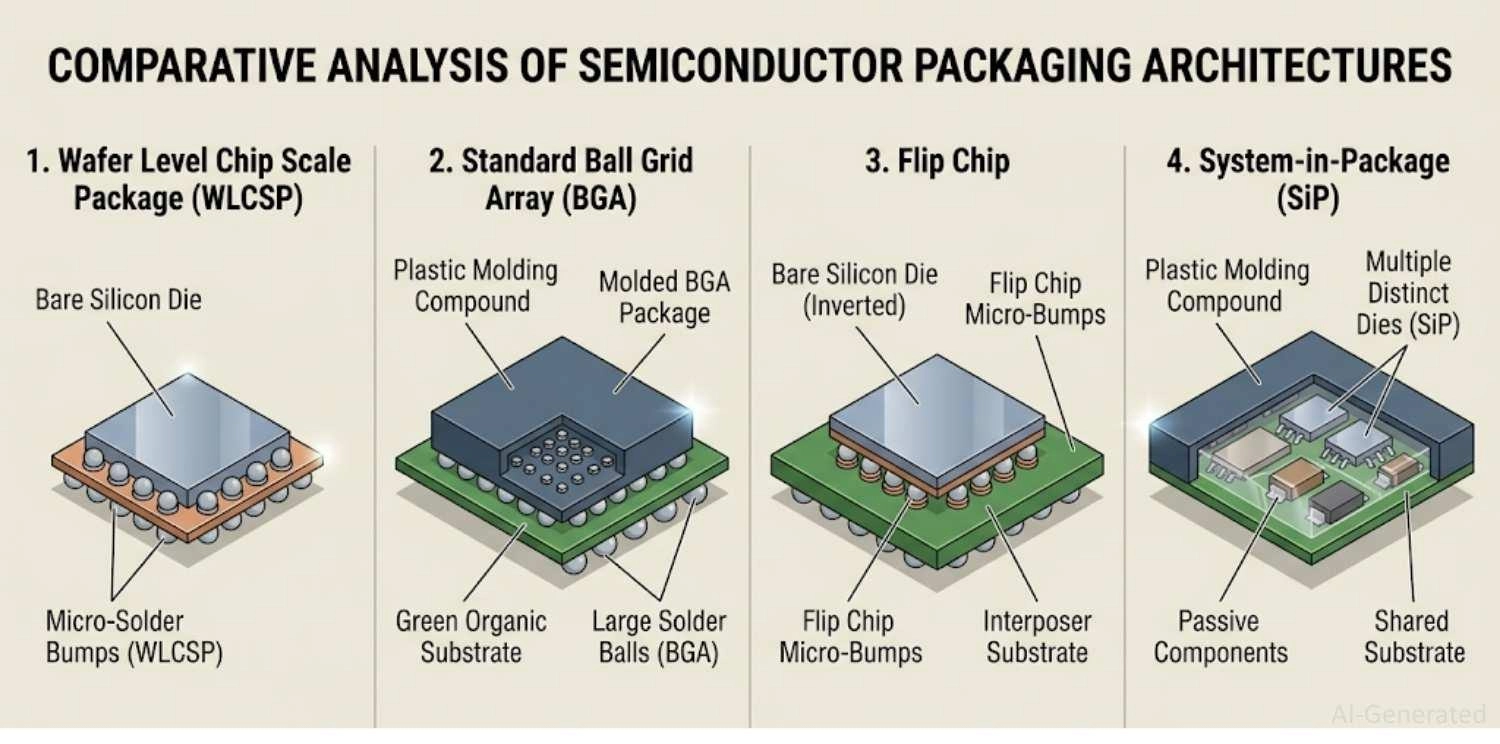
Figure: Comparing WLCSP against standard BGA, Flip Chip, and System-in-Package (SiP) architectures
From Wafer-Level Packaging to PCB Assembly: Bridging Chip Design and Manufacturing
PCB Design Impact and SMT Challenges
Implementing WLCSP PCB design techniques heavily impacts your stackup. High-density interconnect (HDI) PCBs with micro-vias are almost always required to route out of the tight bump arrays.
During SMT assembly, achieving a perfect solder joint is notoriously difficult, requiring strict control over the reflow soldering profile to prevent the fragile silicon from cracking.
Scaling WLP-Based Designs with JLCPCB’s PCB Fabrication and Assembly Services
Whether you are sourcing quality surface mount devices for prototypes or relying on high-precision capabilities, an experienced partner critically impacts manufacturability.
You can leverage JLCPCB’s high-precision PCB assembly to start scaling your projects.
Design Considerations for Engineers Using Wafer Level Packaging
Designing with wafer-level packaging requires careful attention to PCB layout, thermal paths, and signal behavior due to the absence of a protective substrate.
- Footprint Design: Fine pitch (typically 0.3–0.5 mm) demands precise pad geometry and tight tolerances. Errors in alignment or solder mask definition can easily lead to shorts or opens.
- Thermal Management: Heat must be dissipated through the PCB since WLP lacks a heat-spreading substrate. This requires solid ground planes, thermal vias, and optimized copper distribution.
- Signal Integrity: Short interconnects improve performance, but impedance control becomes critical-especially for high-speed and RF signals routed directly under the die.
- Board-Level Reliability (BLR): CTE mismatch between silicon and PCB introduces mechanical stress. Proper pad design, underfill (when needed), and material selection are essential to prevent solder fatigue.
- Assembly Constraints: Accurate stencil design, controlled reflow profiles, and precise component placement are required to ensure reliable solder joint formation.
Designing for WLP is not just about layout-it requires a system-level approach that balances electrical performance, mechanical reliability, and manufacturability.
PCB Design Rules for Wafer-Level Packages (WLP)
Pad Pitch: Typically 0.3-0.5 mm; routing escape often requires HDI stackups with microvias.
Pad Type (NSMD vs SMD): Prefer NSMD (Non-Solder Mask Defined) pads for better solder wetting and fatigue life; keep mask openings slightly larger than copper.
Solder Mask Clearance: Use ~50 µm expansion (process-dependent) to avoid mask encroachment and ensure consistent joints.
Via-in-Pad (VIPPO): Often required for escape routing; vias should be filled and planarized to prevent solder wicking and voiding.
Trace & Spacing: Follow manufacturer limits (e.g., ≤75-100 µm line/space for tight fan-outs); maintain controlled impedance for high-speed nets.
Stencil Design: Optimize aperture size/reduction (often 10-20%) to control paste volume and reduce bridging on fine pitch.
Copper Balancing: Maintain even copper distribution under the device to minimize warpage during reflow.
Underfill (if needed): For harsh environments, apply underfill to improve board-level reliability and mitigate CTE-induced stress.
Placement Accuracy: Tight pick-and-place tolerances are required due to small pad sizes and lack of self-alignment margin.
Adhering to these rules ensures reliable solder joints, manageable routing, and consistent yields in high-density WLP-based designs.
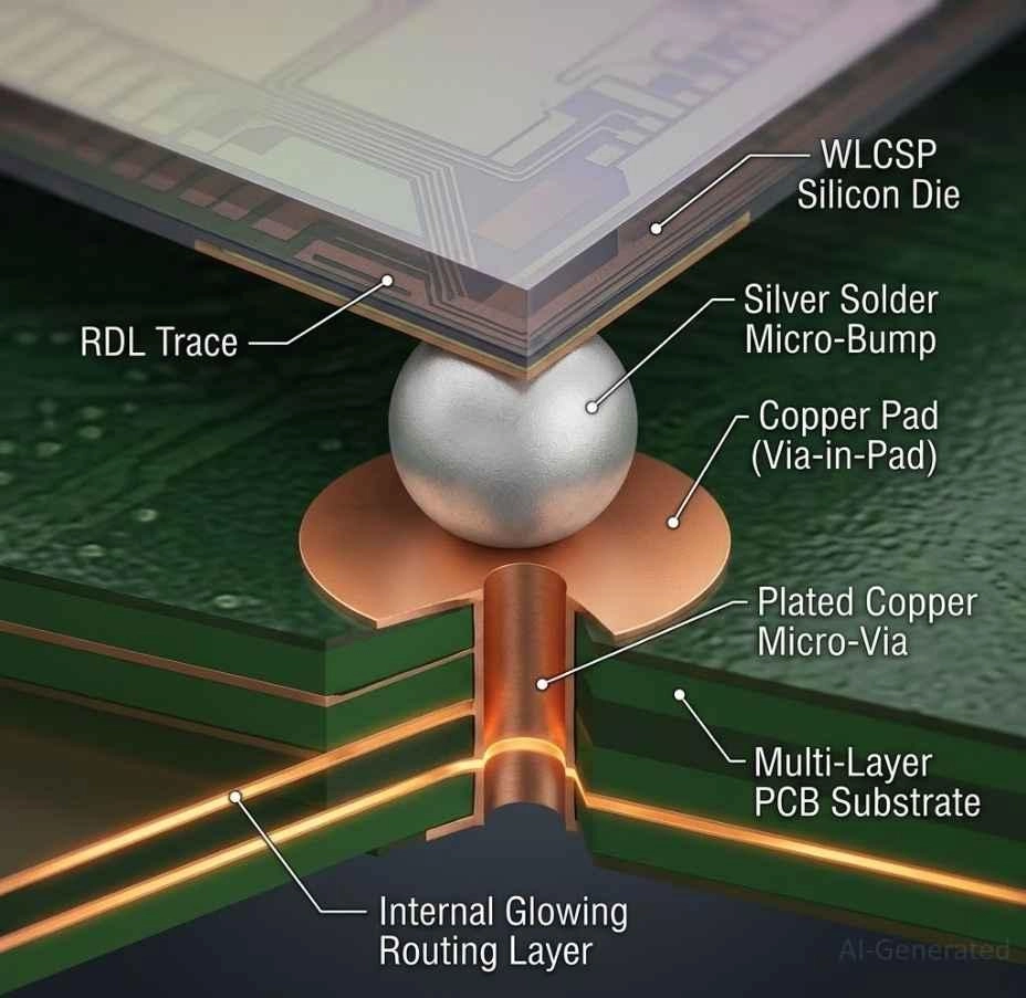
Figure: Micro-via in pad technology used for tight 0.3mm pitch WLCSP layouts
Future Trends in Wafer Level Packaging
Wafer level packaging technology is rapidly evolving to support higher integration, better performance, and continued miniaturization in advanced semiconductor systems.
Fan-Out Growth (FOWLP):
Increasing adoption of fan-out wafer-level packaging to achieve higher I/O density without substrates, enabling thinner and more efficient packages.
Chiplet Integration:
Multi-die architectures are becoming mainstream, where smaller dies are interconnected within a single package to improve yield and scalability.
Heterogeneous Integration:
Combining logic, memory, RF, and analog components in one package to optimize system-level performance and reduce latency.
Advanced RDL Scaling:
Continued reduction in RDL line/space (sub-5 µm) to support higher routing density and improved electrical performance.
AI and High-Performance Computing (HPC):
Growing demand from AI accelerators and HPC systems is pushing WLP toward higher bandwidth and tighter integration.
Companies like Intel are actively developing advanced packaging strategies that leverage these trends to overcome traditional scaling limitations.
FAQ about Wafer Level Packaging
Q: When should engineers choose wafer-level packaging over BGA?
Using the WLP package when minimizing footprint and improving high-frequency performance are critical. However, for high I/O counts or easier PCB routing, BGA may be more practical.
Q: What are the main failure modes of WLP in real products?
The most common failures include solder joint fatigue (especially at corner balls), cracking due to CTE mismatch, and warpage-induced assembly defects.
Q: Why is WLP more sensitive to PCB design than other packages?
Because WLP lacks a protective substrate, mechanical stress is directly transferred to the solder joints, making PCB layout, pad design, and thermal expansion control critical.
Q: What is the typical pitch of WLCSP and why does it matter?
WLCSP pitch typically ranges from 0.3 mm to 0.5 mm. This small pitch increases routing complexity and often requires HDI PCBs with microvias.
Q: Can WLP be used in high-power applications?
Generally, WLP is less suitable for high-power devices due to limited thermal dissipation paths, unless enhanced with underfill or advanced thermal PCB design.
Q: How does fan-out WLP enable chiplet integration?
Fan-out WLP allows redistribution layers to connect multiple dies within a molded package, enabling heterogeneous integration without a traditional substrate.
Conclusion
Understanding the intricacies of wafer-level packaging is no longer optional. As devices demand greater performance in smaller form factors, WLP bridges the gap between silicon limitations and consumer expectations. By mastering the engineering constraints-from HDI routing to DNP awareness-hardware designers can leverage this advanced technology alongside a capable manufacturing ecosystem to build the future of electronics.
Popular Articles
• SMD Diode Code Lookup: Full List, Marking Guide & Identification [2026 Guide]
• SMD Resistor Package Sizes: Complete Size Chart, Footprints & How to Choose
• SMD Capacitor Codes: Identification, Markings, and Polarity
• SMD Capacitor Sizes: Complete Size Chart and Selection Tips for PCB Design and Assembly
• How to Solder SMD Components Like a Pro [2026 Updated]
Keep Learning
PoP Package (Package on Package) Explained: Architecture, Assembly, and SMT Challenges
In the race for miniaturization, fitting more processing power into smaller footprints is the ultimate challenge for PCB designers. Package on Package (PoP) technology answers this by integrating logic and memory vertically, becoming the standard for modern mobile processors. However, this 3D architecture demands advanced SMT assembly capabilities beyond standard fabrication. JLCPCB specializes in the high-precision manufacturing required to master these complex stacks. This guide covers how PoP packa......
What Is a PQFP Package? Plastic Quad Flat Package Design, Footprint, and Assembly Guide
The Plastic Quad Flat Package (PQFP) is a widely used IC package in industrial, automotive, and embedded designs. This article provides a practical, engineering-focused guide to PQFP package. It explains how PQFP is built, when it makes sense to use it, how it compares with newer package types, and what designers should consider in terms of footprint design, thermal performance, signal integrity, manufacturing, and reliability. What Is a PQFP Package (Plastic Quad Flat Package)? A Plastic Quad Flat Pa......
Small Outline Integrated Circuit (SOIC): Package, Specs & Uses
As designs transition from legacy through-hole components to high-density Surface Mount Technology (SMT), the Small Outline Integrated Circuit (SOIC) remains the industry standard for operational amplifiers, flash memory, sensors, and microcontrollers. It stands as a testament to balanced engineering, offering a perfect compromise between the miniaturisation demanded by modern consumer electronics and the ruggedness required for industrial applications. This article serves as a definitive engineering ......
A Complete Guide to Surface Mount Device (SMD)
Imagine holding a smartphone in your hand. Inside that sleek device lies a complex network of thousands of miniature components — resistors smaller than a grain of rice, capacitors thinner than a fingernail, and integrated circuits containing millions of transistors. Without Surface Mount Technology (SMT) and its compact Surface Mount Devices (SMDs), none of this would exist. Just a few decades ago, electronics were bulky. Radios filled desks, computers filled rooms, and assembling a circuit meant dri......
Circuit Breaker Types Explained: MCB, MCCB, RCCB, RCBO, ACB, VCB & SF6 Circuit Breakers
A circuit breaker automatically disconnects power when it detects faults such as overloads or short circuits, protecting equipment and reducing fire risk. Different circuit breaker types are designed for different voltage levels, current ratings, and applications, from household distribution boards to high-voltage substations. This guide explains the most common types - including MCBs, MCCBs, RCCBs, RCBOs, ACBs, VCBs, and SF6 breakers and helps you choose the right one for your application. Figure: Ci......
Quad Flat Package (QFP): The Engineer's Guide to Design, Assembly and Thermal Management
What is QFP Package? The Quad Flat Package (QFP) is one of the most popular surface mount technology (SMT) package formats throughout the history of electronic manufacturing. After it became standard in the 1980s, the QFP has been the industry standard for integrated circuits (ICs) with moderate to high pin counts that typically range from 32 to 304 pins, so it was a good alternative for simple SOIC packages and complex Ball Grid Arrays (BGAs) at the same time. Defined by its "gull-wing" leads extendi......