
Mastering PCB Footprints: Design Best Practices for Reliable Manufacturing
12 min
- What Is a PCB Footprint and Why It Matters
- Main Types of PCB Footprints and Selection Guide
- Best Practices for PCB Footprint Design
- PCB Footprint Design for Manufacturability (DFM)
- From Design to Production: Professional Manufacturing of Precise Footprints
- JLCPCB's Expertise in PCB Footprint Manufacturing
- FAQ about PCB Footprint
- Conclusion on Mastering PCB Footprints
Key Takeaways
- A PCB footprint (land pattern) translates component datasheet dimensions into copper pads, solder mask openings, paste apertures, silkscreen, and clearance areas that enable reliable soldering and assembly.
- Follow IPC-7351 standards and manufacturer DFM rules for pad dimensions, spacing, and layer design to minimize defects like solder bridging, tombstoning, and cracked joints.
- Choose between through-hole (THT) and surface mount (SMT) footprints based on electrical needs, thermal performance, assembly method, and production volume.
- Proper pad sizing, solder mask dams (minimum 0.1 mm), and paste aperture design prevent assembly defects and improve first-pass yield.
- JLCPCB provides one-stop precision fabrication and assembly with tight ±0.1 mm tolerances, verified component libraries, and free DFM analysis tools.
What Is a PCB Footprint and Why It Matters
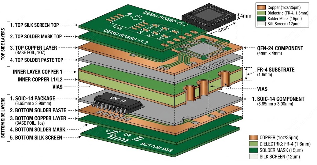
A PCB footprint, also known as a land pattern, is the physical layout that connects an electronic component to the printed circuit board. It translates the mechanical dimensions from a component datasheet into copper pads, solder mask openings, paste apertures, silkscreen markings, and clearance areas that enable reliable soldering and assembly.
Accurate PCB footprints are foundational to successful electronics manufacturing. Even small deviations in pad size, spacing, or alignment can cause defects such as solder bridging, insufficient fillets, tombstoning, or long-term reliability issues like cracked joints under thermal cycling. In high-volume production, footprint-related problems directly affect yield, cost, and time-to-market.
Engineers who invest time in proper PCB footprint design early in the process reduce respins and achieve higher first-pass success rates when working with professional manufacturers.
Definition and Core Components
A complete PCB footprint in EDA tools like EasyEDA or KiCad includes multiple synchronized layers:
- Copper pads: The primary solderable areas, sized according to component leads or terminations.
- Solder mask openings: Slightly larger than pads (typically with 0.05 mm expansion per side at JLCPCB) to account for registration tolerances while maintaining solder dam integrity.
- Solder paste layer: Defines stencil apertures, often reduced relative to pad area to control paste volume.
- Silkscreen: Component outline, reference designator, and polarity/pin-1 indicators.
- Courtyard: A keep-out zone ensuring mechanical clearance during placement and inspection.
These elements must work together. For example, JLCPCB's standard solder mask process uses LPI (Liquid Photo Imageable) mask with a minimum bridge (dam) of 0.1 mm between adjacent pads. Designing pads too close violates this limit and risks mask defects or shorts.
How Accurate Footprints Determine PCB Performance and Reliability
Precise PCB footprints ensure proper solder fillet formation (toe, heel, and side fillets), mechanical strength, and electrical performance. In high-speed or power circuits, footprint geometry affects parasitic inductance, capacitance, and thermal dissipation.
Industry experience shows that footprint inaccuracies contribute significantly to assembly defects. Following standards like IPC-7351 helps standardize calculations for pad dimensions based on component tolerances and density levels (Least, Nominal, Most).
At JLCPCB, overall dimension tolerance is ±0.1 mm, and minimum annular ring for reliable vias and holes is typically 0.15 mm or greater to accommodate drill wander and plating requirements. Insufficient annular rings risk breakout and open circuits, especially under mechanical stress or thermal expansion.
Main Types of PCB Footprints and Selection Guide
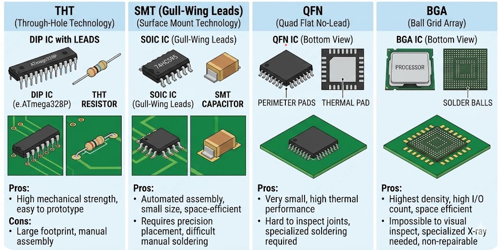
Through-Hole (THT) Footprints
THT footprints feature drilled holes surrounded by annular ring pads. They are preferred for connectors, large power components, and parts requiring strong mechanical attachment.
Key parameters include hole diameter (usually 0.1–0.3 mm larger than the lead), pad diameter (providing adequate annular ring), and thermal relief spokes for planes. JLCPCB supports minimum drilled hole sizes around 0.2 mm with recommended annular rings of 0.15–0.3 mm depending on the application for reliable plating and strength.
Proper THT design prevents issues like insufficient hole fill or pad lifting during wave or hand soldering. Thermal relief designs must balance heat dissipation during soldering with electrical performance in power planes.
Surface Mount (SMT) Footprints: QFN, BGA, Gull-Wing and More
SMT footprints dominate modern high-density designs.
- Gull-wing packages (SOIC, QFP, TSSOP) have extended leads allowing visible heel-and-toe fillets and easier inspection/rework.
- QFN and DFN use bottom-terminated pads with exposed thermal centers, requiring segmented paste patterns and thermal vias to minimize voids.
- BGA and LGA demand precise ball-pad sizing, via-in-pad options, and careful standoff control.
JLCPCB supports advanced features like via-in-pad (filled and capped on higher layer counts) to enable denser routing under these packages.
Choosing the Right Footprint for Your Application
Selection balances electrical needs, thermal performance, assembly method, and volume. For prototypes, prioritize hand-solder-friendly layouts with larger pads. For automated high-volume production, optimize for SMT process windows using IPC-7351 guidelines and manufacturer DFM rules.
Always start with the component datasheet's recommended land pattern, then adapt for density and JLCPCB capabilities such as minimum 0.1 mm solder mask bridge and ±0.1 mm tolerances. Consider inspection access, reworkability, and signal integrity requirements before finalizing.
Best Practices for PCB Footprint Design
IPC Standards and Critical Design Parameters
IPC-7351 serves as the primary reference for land pattern design. It provides formulas for pad width (X), gap (G), and overall length (Z) while accounting for component tolerance, solder fillet goals, and placement accuracy.
Engineers should verify library parts against the latest datasheet rather than trusting defaults. Cross-check pin 1 orientation, polarity, and 3D body models to prevent assembly errors.
Pad Size, Spacing, Solder Mask, and Paste Design Rules
Optimal pad dimensions balance solder volume for strong joints without risking bridges. For fine-pitch components, maintain sufficient gap to support JLCPCB's 0.1 mm minimum solder mask dam.
| Pad Width (mm) | Pad Length (mm) | Min Solder Mask Bridge | Paste Aperture Reduction | |
|---|---|---|---|---|
| 0402 Resistor/Cap | 0.50–0.60 | 0.55–0.70 | 0.1 mm | 80–90% |
| QFN 0.5 mm pitch | 0.25–0.30 | 0.60–0.80 | 0.1 mm | 60–70% (segmented) |
| SOIC-8 Gull Wing | 0.60–0.65 | 1.80–2.00 | 0.1 mm | Standard |
| QFP 0.5 mm pitch | 0.24–0.28 | 1.50–1.70 | 0.1 mm | 5–10% |
Table 1: Typical SMT Footprint Parameters Aligned with IPC & JLCPCB Capabilities
Common Design Errors and How to Prevent Them
Common Footprint Mistakes
- Mirrored footprints causing incorrect component orientation
- Incorrect pin numbering, especially for bottom-view packages
- Inadequate courtyard clearance leading to placement interference
- Mismatched paste and mask layers resulting in soldering defects
Prevention strategies: Use verified libraries (such as those from LCSC/JLCPCB), enable 3D viewing, run full DRC against manufacturer rules, and utilize JLCPCB's free JLCDFM tool before ordering. Double-check datasheet mechanical drawings and perform a paper print test for critical packages.
PCB Footprint Design for Manufacturability (DFM)
Impact of Footprint Design on Assembly Yield and Cost
Good PCB footprint design directly improves first-pass yield and lowers overall project cost. Poorly optimized pads increase defects like bridging or insufficient solder, leading to higher rework and scrap rates.
Standardized, manufacturer-aligned footprints reduce engineering time and allow better utilization of automated SMT lines.
Fine-Pitch, High-Density and Thermal Management Challenges
Fine-pitch components (0.4–0.5 mm) leave little margin for error. Maintain aspect ratios in stencil apertures and use thermal vias under exposed pads (e.g., QFN center pads) connected to copper planes. JLCPCB supports via-in-pad technology to free routing space while managing heat in dense layouts.
Ensuring Signal Integrity Through Proper Footprint Layout
Symmetric pad placement and short, matched trace lengths help maintain signal integrity for high-speed and differential pairs. Ground plane stitching around footprints reduces EMI and provides low-inductance return paths. Avoid unnecessary stubs and consider impedance continuity from pad to trace.
From Design to Production: Professional Manufacturing of Precise Footprints
Advanced Fabrication Capabilities for Complex Footprints
Professional PCB manufacturers transform digital PCB footprint designs into physical boards using high-precision processes capable of handling fine-pitch, high-density, and multi-layer requirements. JLCPCB supports up to 32 layers with tight overall dimension tolerances of ±0.1 mm, enabling complex footprints in HDI designs.
Capabilities such as controlled impedance (±10%) and advanced via technologies allow engineers to implement dense BGA and QFN layouts without compromising routing or signal performance. These fabrication strengths ensure that even intricate PCB footprint geometries — including fine pads and thermal structures — translate accurately from Gerber files to finished boards.
Precision Processes: Etching, Plating and Solder Mask Alignment
The fabrication journey begins with precise etching to define copper pads within tight tolerances, followed by electroplating to ensure reliable conductivity and robust annular rings. JLCPCB maintains minimum annular rings around 0.15 mm for vias and holes to prevent breakout despite drill registration variations.
Solder mask application is equally critical. Using LPI solder mask, JLCPCB applies a standard expansion of 0.05–0.1 mm per side and supports a minimum 0.1 mm solder mask bridge between pads. Precise alignment during exposure and development prevents mask encroachment on pads or insufficient dams that could lead to solder shorts. These controlled processes ensure PCB footprint features like pad geometry and clearances remain consistent across production runs.
SMT Assembly Excellence: Stencil and Placement Accuracy
SMT assembly quality depends heavily on stencil precision and placement accuracy. JLCPCB utilizes laser-cut stainless steel stencils with positioning accuracy of ±0.003 mm and optional nano-coating for superior paste release and reduced bridging. Stencil thickness (commonly 0.1–0.12 mm) and aperture designs are optimized based on the PCB footprint paste layer to achieve ideal solder volume.
Automated pick-and-place machines combined with carefully profiled reflow ovens deliver repeatable results across gull-wing, QFN, BGA, and other package types. For hidden joints, X-ray inspection verifies fill and void rates.
| Typical / Minimum Value | Benefit for Footprint Design | |
|---|---|---|
| Dimensional Tolerance | ±0.1 mm | Predictable pad geometry and placement |
| Solder Mask Bridge (Dam) | 0.1 mm | Enables fine-pitch layouts without shorts |
| Solder Mask Expansion | 0.05–0.1 mm per side | Reliable solder fillet formation |
| Minimum Annular Ring | 0.15 mm | Prevents breakout on vias and THT pads |
| Stencil Cutting Precision | ±0.003 mm | Consistent paste volume and reduced defects |
| Via-in-Pad Support | Free on 6–20 layers | Higher density routing under components |
Table 2: JLCPCB Key Manufacturing Capabilities Supporting Precise PCB Footprints
JLCPCB's Expertise in PCB Footprint Manufacturing
1One-Stop Fabrication and Assembly with Optimized Footprint Processes
JLCPCB provides a seamless one-stop service for PCB fabrication and SMT assembly, with processes specifically tuned to common footprint design rules. This integration eliminates handoffs between vendors and ensures that PCB footprint details — from pad dimensions to paste patterns — are handled consistently from prototype to production.
Engineers benefit from rapid turnaround options and scalable manufacturing that supports everything from quick prototypes to medium-to-high volume runs.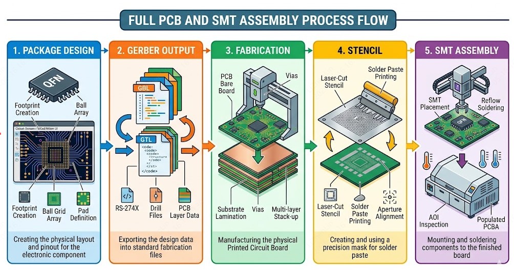
2Verified Component Libraries and Tight Tolerance Control
Through its partnership with LCSC, JLCPCB offers access to a vast library of verified components where footprints are pre-aligned with actual manufacturing capabilities. This reduces the risk of library mismatches and saves design time.
Tight process controls give designers confidence when implementing dense or high-reliability PCB footprints.
3Quality Assurance Ensuring First-Pass Success
Comprehensive quality systems at JLCPCB include automated optical inspection (AOI), X-ray examination for hidden joints, and electrical testing where required. Free DFM analysis tools flag potential footprint-related issues before production begins.
These measures help achieve high first-pass yields and consistent quality across orders.
FAQ about PCB Footprint
Q: What is a PCB footprint?
A PCB footprint, also called a land pattern, is the physical layout on a PCB that connects an electronic component to the board. It includes copper pads, solder mask openings, paste apertures, silkscreen markings, and clearance areas that together enable reliable soldering and assembly.
Q: What is the difference between THT and SMT footprints?
Through-hole (THT) footprints use drilled holes with annular ring pads and are preferred for connectors and large power components requiring strong mechanical attachment. Surface mount (SMT) footprints mount components directly on the board surface, enabling higher density and automated assembly. SMT types include gull-wing (SOIC, QFP), bottom-terminated (QFN, DFN), and ball grid array (BGA) packages.
Q: What are the most common PCB footprint design mistakes?
Common mistakes include mirrored footprints, incorrect pin numbering (especially for bottom-view packages), inadequate courtyard clearance, mismatched paste and mask layers, and pads designed too close without sufficient solder mask dams. Using verified libraries, running DRC checks, and consulting JLCPCB's free DFM tools can help prevent these errors.
Q: How does footprint design affect manufacturing yield?
Footprint-related issues directly impact first-pass yield. Poor pad geometry can cause solder bridging, insufficient fillets, tombstoning, or long-term reliability issues. Standardized, manufacturer-aligned footprints reduce defects and rework costs, while optimized designs ensure consistent paste volume and reliable joint formation.
Q: What IPC standard governs PCB footprint design?
IPC-7351 is the primary standard for land pattern design. It provides formulas for pad width (X), gap (G), and overall length (Z) while accounting for component tolerances, solder fillet goals, and placement accuracy. The standard defines three density levels — Least, Nominal, and Most — to suit different application requirements.
Conclusion on Mastering PCB Footprints
Mastering PCB footprints requires combining datasheet details, IPC standards, and real manufacturing constraints. By designing with DFM in mind — proper pad geometry, adequate clearances, thermal management, and verified libraries — engineers create boards that perform reliably from prototype to production.
Partnering with an experienced manufacturer like JLCPCB bridges the gap between design intent and physical reality. Their precision capabilities, one-stop service, and quality focus help turn well-crafted PCB footprints into high-reliability electronic products.
Review your footprints against current capabilities, run DFM checks early, and leverage professional fabrication and assembly for the best outcomes on your next project.
Popular Articles
Keep Learning
How to Design Your Own Keyboard PCB: From Layout to Firmware
Designing a custom keyboard PCB is one of the most rewarding entry points into practical electronics. You not only get a really useful product on your desk, but also you learn schematic capture, matrix scanning, footprint selection, USB, and firmware. Most of the hardware engineers use the same skills that show up on professional boards. This guide walks the entire build from choosing switches, wiring the diode matrix, adding the microcontroller and USB-C, laying out the board, and flashing QMK or VIA......
Don't Let Design Errors Ruin Your Hardware: The Complete Guide to PCB Design Verification
Key Takeaways PCB design verification is the systematic process of validating layouts against electrical, signal integrity, and manufacturing rules before production, preventing costly board respins and launch delays. Schematic verification through Electrical Rules Check (ERC) catches floating inputs, power shorts, and footprint mismatches before layout begins. Design Rule Checking (DRC) ensures trace widths, clearances, and via sizes comply with your fabricator's manufacturing tolerances, especially ......
How to Determine the Right PCB Voltage Clearance for Safe and Reliable Designs
Key Takeaways Clearance is the air gap; Creepage is the surface path — both essential for high-voltage safety. Base spacing on peak voltage and follow IPC-2221 / IEC 60664-1 standards. Major factors: voltage, pollution degree, CTI, altitude, and conductor location. Use isolation slots, guard rings, and conformal coating to optimize spacing. Always run clearance calculations, DFM checks, and Hipot testing before production. Why do two copper traces that work fine at 5V suddenly arc over and burn at 400......
Mastering PCB Footprints: Design Best Practices for Reliable Manufacturing
Key Takeaways A PCB footprint (land pattern) translates component datasheet dimensions into copper pads, solder mask openings, paste apertures, silkscreen, and clearance areas that enable reliable soldering and assembly. Follow IPC-7351 standards and manufacturer DFM rules for pad dimensions, spacing, and layer design to minimize defects like solder bridging, tombstoning, and cracked joints. Choose between through-hole (THT) and surface mount (SMT) footprints based on electrical needs, thermal perform......
How Copper Thieving Balances Your PCB for Better Manufacturing Results
Key Takeaways Copper thieving adds non-functional copper patterns (dots, squares, or crosshatch) to balance copper density across PCB layers. This effectively reduces uneven plating (from 20-30% to <10%), board warpage, inconsistent etching, and impedance issues, delivering tighter tolerances, better solder mask adhesion, higher yields, and lower costs. For best results, target 40-60% copper density per layer, maintain proper clearances, and ensure stackup symmetry. When done right, it transforms comp......
ZIF Connectors Simplify Flexible PCB Assembly with Tool-Free Reliability
Did you ever attempt to mate a fragile flex cable into a connector and experience that unpleasant resistance, and wonder whether you were tearing off the tail or breaking the casing? It is precisely that tension that the ZIF connectors were supposed to help remove. Zero insertion force technology allows you to slide a flexible printed circuit or flat flexible cable into the receptacle to be mated with, using almost no push force at all, but rather allows a mechanical actuator to hold the cable firmly ......