How to Solder QFN Components: A Step-by-Step Guide
14 min
- Quick Answer: How to Solder QFN Components
- Why QFN Soldering Is Hard: Hidden Pads and the Thermal Pad
- What You Need to Solder QFN Components
- The QFN Stencil: Thermal-Pad and Fine-Pitch Essentials
- How to Solder QFN With Paste, a Stencil, and Reflow
- How to Hand-Solder a QFN Without Hot Air
- Avoiding QFN Voiding and Common Soldering Defects
- FAQ about Soldering QFN Components
- Conclusion: Soldering QFN Components With Confidence
Key Takeaways
- A solder paste stencil is the most reliable way to achieve consistent QFN solder joints.
- Always use a window-pane paste pattern on the center thermal pad instead of one large paste deposit.
- Control solder paste volume to prevent floating, bridging, and excessive voiding.
- Reflow needs a proper soak-then-reflow-then-cool profile
- Hand soldering is practical only for certain QFN packages and usually cannot solder the center thermal pad effectively.
- Because QFN solder joints are hidden beneath the package, inspect them using continuity testing, test points, or X-ray where appropriate.
QFN packages deliver excellent size, thermal, and RF performance, but every pad, including the wide thermal pad at the center, sits hidden underneath the package body. A soldering iron alone often can’t reach them, so first attempts often end in shorts, opens, or a chip that “floats” off its pads during reflow.
This guide shows how to solder QFN components reliably, whether by stencil-and-reflow or by careful hand soldering, and how to dodge the classic defects that mostly show up after the joints are already sealed. If you require fundamental QFN package classifications, land pattern dimensions, or footprint rules, explore our QFN package guide.
Quick Answer: How to Solder QFN Components
To solder QFN components, apply solder paste through a stencil using a window-pane pattern on the thermal pad, place the package accurately with tweezers, then reflow it using a hot plate, hot air station, or reflow oven. For QFNs with side-castellated or wettable flanks, careful perimeter hand soldering using flux and a chisel tip is also achievable.
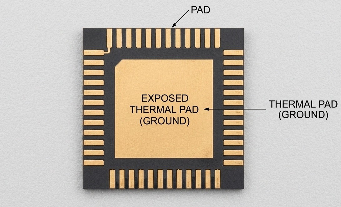
Why QFN Soldering Is Hard: Hidden Pads and the Thermal Pad
QFN soldering is unforgiving mainly because you can’t see or directly reach the joints once the component is sitting on the board. Unlike a leaded package, there are no exposed leads to touch with a soldering iron. Surface tension helps the package settle into alignment during reflow, but the same force can pull excess solder into neighboring pads and create bridges. The large exposed thermal pad underneath the package adds another variable: too much solder there can lift the QFN slightly and prevent the perimeter pads from making proper contact.
The Exposed Thermal Pad Problem
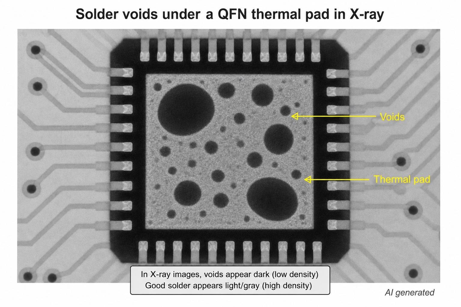
Print too much paste under the thermal pad and the QFN can “float” or stand off unevenly, preventing the perimeter pads from making proper contact. Print it as one solid deposit and the flux trapped underneath has fewer paths to escape, it turns into trapped gas that shows up as voids on an X-ray later, this reduces the effective thermal and electrical contact beneath the package. A window-pane pattern, covered below, addresses both problems at once.
Fine-Pitch Perimeter Pads
At 0.5 mm and especially 0.4 mm pitch, the gap between adjacent perimeter pads leaves almost no margin for error. A smear of extra paste, an oversized aperture, or paste that clings to the stencil wall instead of releasing cleanly is enough to bridge two pins. In practice, paste volume and release, not reflow temperature, is usually the real variable that decides whether fine-pitch QFNs print clean. The QFN package guide covers the footprint and land-pattern math behind these pad sizes in more depth.
What You Need to Solder QFN Components
- No-clean tacky flux: Once the part is down, there’s no way to clean flux out from underneath it.
- Fine solder or Type 3–4 solder paste: Finer particles print more evenly through small apertures.
- ESD-safe tweezers or a vacuum pick: For placing a part you can’t nudge into alignment with an iron afterward.
- A heat source: Hot air, a hot plate, or a reflow oven, matched to the job.
- Magnification or a USB microscope: Pin-1 orientation and bridge detection are hard to judge with the naked eye at 0.4–0.5 mm pitch.
- A solder paste stencil: For anything fine-pitch or with a center pad, hand-dosing paste isn’t realistic.
The Case for a Stencil (Even for One QFN)
It can be tempting to apply paste manually, especially when you’re assembling just one QFN. But trying to hand-dose paste onto a hidden thermal pad and 0.4 mm perimeter pads is largely guesswork. A stencil deposits a repeatable, controlled volume across the entire footprint in one pass, making it much easier to keep the paste amount consistent from pad to pad. For one-off prototypes, a precision stencil from a manufacturer such as JLCPCB can still be a practical option when consistent paste deposition matters.
The QFN Stencil: Thermal-Pad and Fine-Pitch Essentials
Window-Pane the Thermal Pad
The one rule to get right when soldering a QFN is never print the thermal pad as a single large opening. Split it into a segmented “window-pane” pattern that covers roughly 50–70% of the pad area, in guidance that aligns with Microchip’s AN18.15 QFN and DQFN design app note, the standard covering design and assembly for bottom-termination components. Breaking the paste into smaller deposits gives flux gases room to escape during reflow, reduces the amount of solder beneath the package, and helps prevent the QFN from floating while still maintaining good thermal contact.
If the pad has thermal vias underneath, web the stencil openings around them so paste doesn’t wick down into the board instead of staying on the pad. For the exact grid sizing, area ratios, and reduction percentages for a specific pad size, the SMT Stencil Design Tips and How to Choose a Solder Paste Stencil articles cover the formulas in more depth than we will here.
Clean Paste Release on Fine Pitch (Why Coatings Matter)
Once you move to 0.4 mm and 0.5 mm pitch QFNs, depositing the right amount of solder paste becomes less about heat and more about whether the paste releases cleanly from the stencil. A rough-walled aperture typical of a chemically etched or poorly finished stencil holds paste back on the walls instead of letting it drop cleanly onto the pad, leading to starved, inconsistent deposits.
Two finishing steps address this directly. Electropolishing smooths out the micro-burrs left behind by laser cutting, and a nano-coating adds a low-friction layer so paste releases in one clean motion and the underside of the stencil stays cleaner between prints. JLCPCB, as one worked example, laser-cuts stencils to ±0.003 mm and offers both finishes at low added cost.
If you’d like to explore the aspect-ratio and area-ratio math behind exact reduction percentages as per IPC-7525, our SMT Stencil Design Tips cover the design considerations in detail.
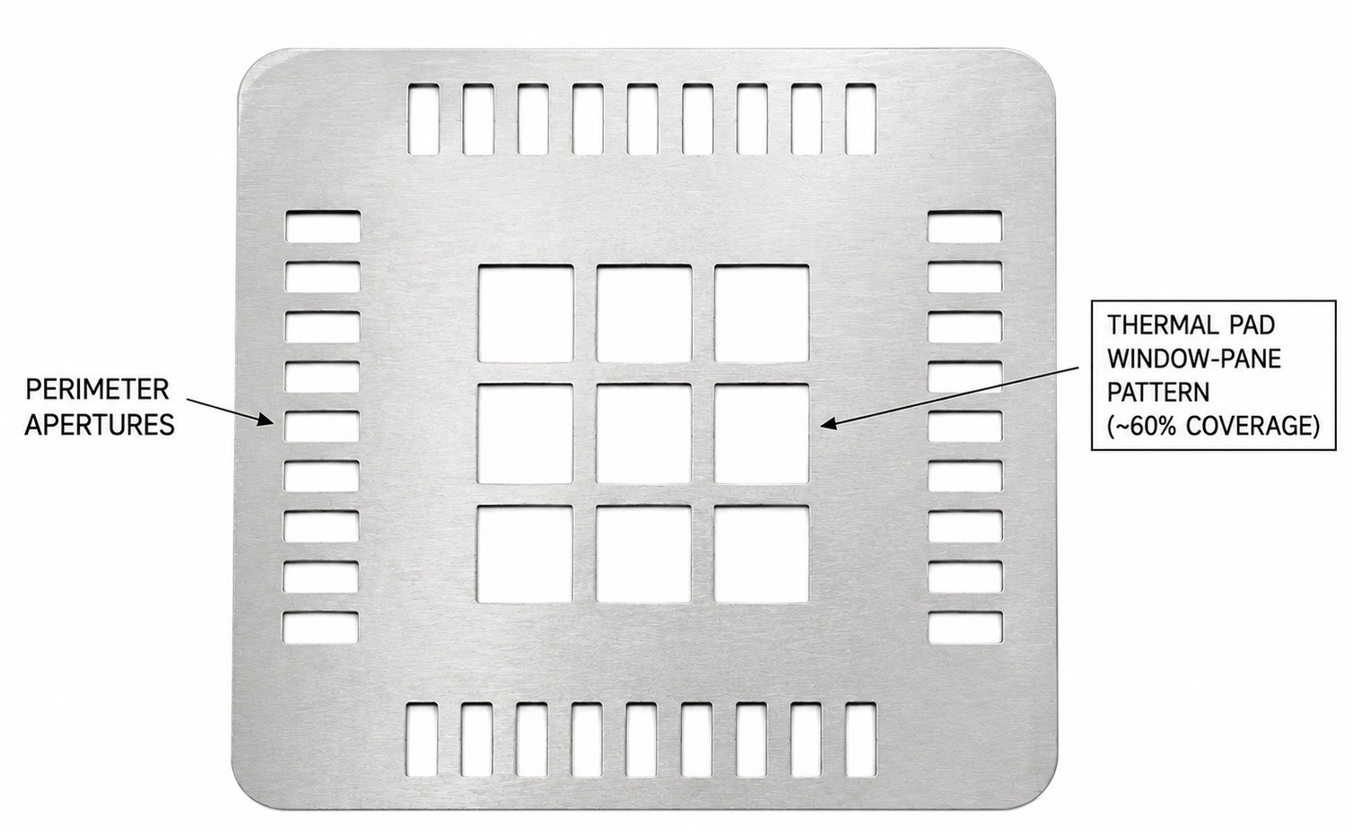
Window-pane stencil apertures for a QFN thermal pad
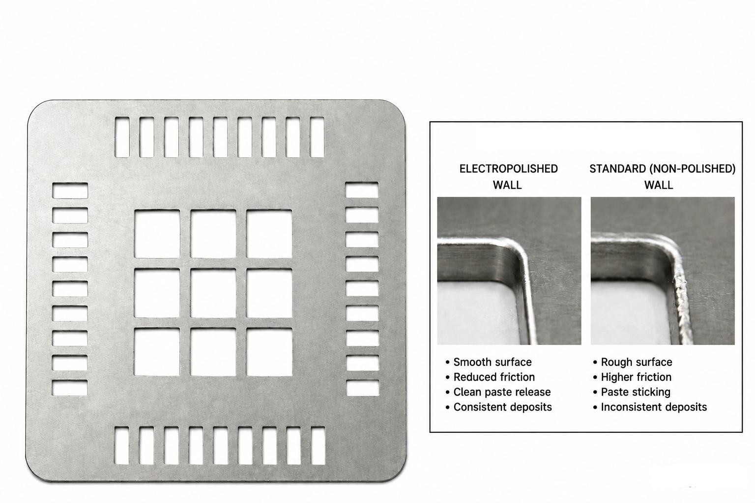
Electropolished stencil aperture wall for clean release
How to Solder QFN With Paste, a Stencil, and Reflow
- Print: Tape or jig the board flat, align the stencil to the pads using fiducials where available (see the SMT stencil fiducials guide), squeeze paste across at roughly a 45° angle, and lift the stencil straight up. Inspect the deposits before moving on, perimeter pads should look like clean, distinct “bricks,” and the thermal pad should show the window-pane pattern rather than one solid smear.
- Place: Set the QFN with tweezers or a vacuum pick, align pin-1 to the footprint marking, and let go. The paste’s tack holds the part in place, pressing down only squeezes paste out from under the pads.
- Reflow: Heat the board on a hot plate, with hot air, or in a reflow oven, following a soak-then-reflow-then-cool profile rather than blasting straight to peak temperature (the reflow profile guide covers the curve in detail). Peak temperature depends on the alloy. Sn63Pb37 profiles typically peak around 210–225°C, while lead-free SAC305 profiles run higher, around 235–250°C. Cooling should ramp down gently rather than dropping abruptly, since a sudden swing can warp a board carrying a QFN’s heavy thermal pad.
- Self-alignment: As the solder melts, surface tension pulls the part gently toward the center on its pads. Some drift toward alignment during reflow is normal and a good sign; a part that’s badly skewed going in may not fully correct itself.
Hot Air vs. Hot Plate vs. Reflow Oven: Which to Use?
| Method | Best For | Pros | Cons | QFN-Specific Notes |
|---|---|---|---|---|
| Hot Air Station | Rework or a single QFN | Precise, localized heat; no oven needed | Can blow small passives off the board | Easy to heat the thermal pad unevenly versus the perimeter |
| Hot Plate | Small prototypes, single-sided boards | Even bottom heat; low cost | Can't reach double-sided or top-heavy boards | Large thermal pad heat-sinks the board, slowing local reflow |
| Reflow Oven | Whole boards or small batches | Precise, multi-zone thermal profiling; repeatable high quality. | Higher cost; needs a defined profile | Best option for QFN thermal pads. Prevents thermal shock and minimizes voids across large exposed ground planes. |
Use a Hot Plate for fast single-sided prototype builds, a Hot Air Station for single IC rework, and a Reflow Oven for multi-component or double-sided production runs.
Inspection After Reflow
Because QFN joints are hidden under the package, a visual scan alone can’t confirm a good solder joint. Continuity checks and dedicated test points catch electrical opens and shorts; X-ray or automated optical inspection is the production standard, since it’s the only reliable way to see voiding under the thermal pad. QFNs with wettable flanks (side-castellated leads) are the exception; those show a visible fillet at the package edge that can be checked under magnification.
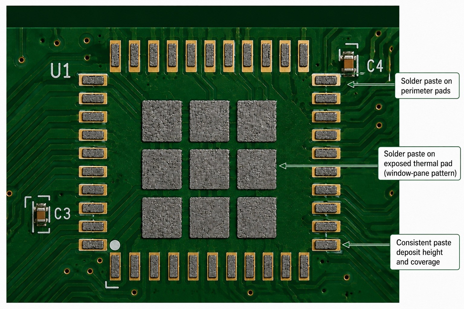
Solder paste printed on a QFN footprint with a stencil
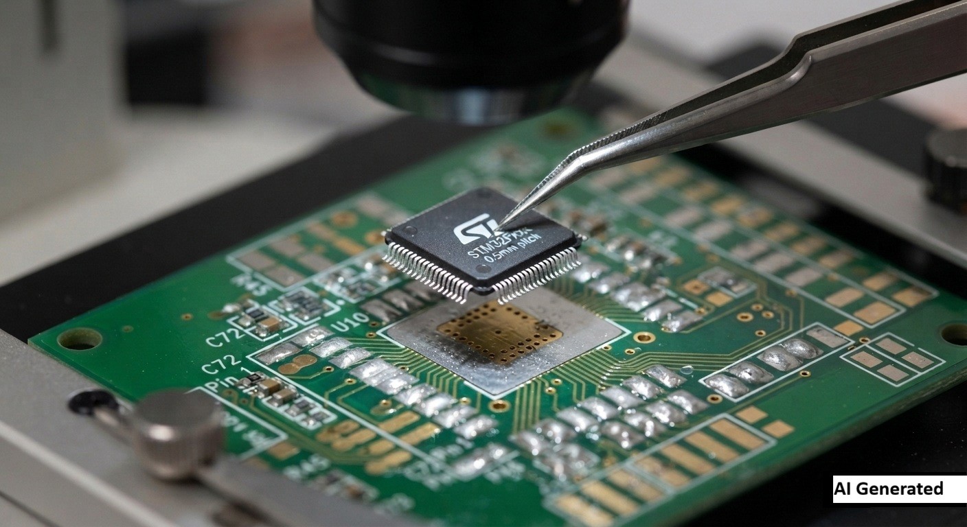
Placing a QFN onto pasted pads before reflow
How to Hand-Solder a QFN Without Hot Air
An iron-only approach works for QFNs with side-castellated, wettable-flank leads or larger pitch, and specifically for the perimeter pins. Once you move to very fine-pitch QFNs or packages with a large exposed thermal pad, an iron-only approach becomes much less reliable because you can’t properly heat or inspect the hidden joints beneath the package.
- Technique: Flux the pads generously, tin them lightly, tack one corner of the part to hold alignment, then drag- or point-solder along the remaining perimeter pins. Clear any bridges afterward with extra flux and solder wick.
- Thermal-pad workaround: If the layout brings the thermal pad out to vias accessible from the back side, it’s possible to solder the pad through those vias with an iron. Otherwise, a stencil and reflow remain the dependable route for that pad.
- Set expectations: QFN hand soldering is fine for one-off repairs and low-pin-count prototypes. It isn’t realistic for fine pitch or any kind of volume at that point; a proper stencil-and-reflow setup, or handing the board to a professional assembly house, is the better use of time.
Avoiding QFN Voiding and Common Soldering Defects
- Voiding under the thermal pad: Caused by flux gas trapped under a solid paste deposit with nowhere to escape. Fixed with window-pane apertures plus a reflow profile that gives paste enough soak time to outgas before it solidifies.
- Bridging on perimeter pins: Usually too much or smeared paste combined with an oversized aperture. Fixed with aperture reduction relative to the copper pad, smoother aperture walls (electropolished or nano-coated), and a controlled, even squeegee pass. The solder paste printing defects guide covers more failure patterns and fixes.
- Floating or tombstoning: Excess paste on the center pad lifts the part on a cushion of solder during reflow. Fixed by cutting thermal-pad coverage to roughly 50–70% instead of printing it solid.
- Starved or open joints: Paste wicking away into open thermal vias instead of staying on the pad. Fixed by tenting or plugging the vias and double-checking deposit volume during inspection.
Most of these defects trace back to the paste-printing step — get that right with a precise stencil and a controlled profile, and the rest of the process tends to follow. Void limits vary by standard and class; IPC-7093 and IPC-A-610 are the references worth checking against whatever your process or customer specifies.
FAQ about Soldering QFN Components
Q: Can You Solder a QFN With a Soldering Iron?
Yes, for QFNs with wettable, side-castellated flanks or larger pitch, and for the perimeter pins generally — those give an iron tip something to reach. The center thermal pad and very fine pitch are the hard parts, since there’s no exposed lead to touch. If the board routes thermal vias out to the back side, you can sometimes solder the pad through them; otherwise, stencil-and-reflow is the more dependable method for that connection.
Q: Do I Need a Stencil for QFN Soldering?
It’s strongly recommended for fine pitch and for the thermal pad specifically. Hand-dosing paste under a hidden pad is largely guesswork — too much floats the part, too little starves the joint. A stencil deposits an engineered, repeatable volume across every pad in one pass, which is what actually keeps floating, bridging, and voiding under control on a part this small.
Q: How Much Solder Paste Should Go on a QFN Thermal Pad?
Aim for roughly 50–70% paste coverage using a segmented window-pane pattern, not a solid deposit across the whole pad. Printing the full area 1:1 traps flux gas with nowhere to vent and deposits far more solder volume than the joint needs, both of which raise the risk of voiding and a part that floats during reflow.
Q: Why Does My QFN Float During Reflow?
A QFN usually floats because there’s too much solder paste beneath the center thermal pad. As the solder melts, surface tension lifts the package slightly, preventing the perimeter pads from settling properly onto the PCB. Cutting thermal-pad coverage to the window-pane range and verifying deposit volume during inspection usually solve the problem.
Q: Can I Rework a QFN Without Removing It?
Sometimes a single bridged or lifted perimeter joint can often be reflowed in place with hot air and fresh flux. But because most of the joints, and the entire thermal pad, are hidden under the package, anything beyond a minor edge fix usually needs the part removed and re-pasted properly.
Q: What's the Best Stencil Thickness for a 0.5 mm Pitch QFN?
For most 0.5 mm pitch QFN packages, a stencil thickness of around 0.10–0.12 mm provides a good balance between paste volume and paste release. The ideal thickness also depends on the aperture design, component geometry, and PCB layout, so it should be considered together with stencil aperture optimization rather than as a fixed value. The stencil-design guides cover that balance in more detail.
Conclusion: Soldering QFN Components With Confidence
QFN soldering is fundamentally a paste-and-heat problem, not an iron problem. Once the thermal pad is windowed correctly and the perimeter apertures are sized to release paste cleanly, a controlled reflow profile turns what looks like an intimidating part into a routine one.
For fine-pitch boards, using a precise, cleanly releasing stencil, especially one with electropolished aperture walls or a nano-coating, helps remove most of the remaining risk. And when the design is too dense, or the assembly volume grows, professional PCB assembly is often the simplest way to achieve consistent, production-quality results.
Keep Learning
How to Solder SMD LEDs: A Step-by-Step Guide for Iron, Hot Air, and Reflow
Key Takeaways Confirm polarity and orientation first: Identify the anode and cathode before applying any heat, because a reversed SMD LED will not light and correcting it costs another thermal cycle. Match the method to the job: A fine-tip iron suits one or a few LEDs, hot air is best for rework and single-part replacement, and solder paste with reflow is fastest for complete boards. Keep solder and heat minimal: A small, fully wetted fillet and short dwell times protect the LED die, phosphor, and enc......
How to Solder a Potentiometer (PCB, Panel & Guitar Pots)
Key Takeaways Identify the wiper terminal: In most potentiometers, the middle pin is the wiper. Always verify with a multimeter before soldering. Pre-tin surfaces: Tin both the terminals and wires before joining to ensure strong, clean solder joints. Control heat carefully: Use a temperature-controlled iron and keep contact time short (below 260°C for a few seconds) to avoid damaging the internal resistive track. Test after soldering: Always check continuity and sweep the shaft while measuring output ......
How to Solder QFN Components: A Step-by-Step Guide
Key Takeaways A solder paste stencil is the most reliable way to achieve consistent QFN solder joints. Always use a window-pane paste pattern on the center thermal pad instead of one large paste deposit. Control solder paste volume to prevent floating, bridging, and excessive voiding. Reflow needs a proper soak-then-reflow-then-cool profile Hand soldering is practical only for certain QFN packages and usually cannot solder the center thermal pad effectively. Because QFN solder joints are hidden beneat......
How to Solder Pin Headers: A Step-by-Step Guide
Key Takeaways Breadboard or jig: Use a breadboard or jig to hold the header pin square while you work. Tack one pin first: Check alignment before soldering the rest. Keep heat brief: So the plastic housing doesn't melt. Cut breakaway strips: Score the plastic between pins, not by forcing a cut mid-pin. SMD headers: Soldered with paste and reflow rather than through-hole technique. Desolder a pin: Add fresh solder plus wick or a pump, or use hot air. Introduction You solder a header pin, look at it, an......
Hot Air Surface Mount Soldering: A Step-by-Step Guide
Key Takeaways Heat Control Is Everything: Hot air SMD soldering delivers uniform heat across all pads simultaneously, eliminating the lifted pads and cold joints common with iron-based soldering of fine-pitch components. Airflow Kills Small Parts: Set airflow to just 10–20% for 0402/0201 passives to avoid the Bernoulli Effect that turns tiny resistors into projectiles. Stencil Precision Prevents Tombstoning: A precision-cut SMT stencil deposits equal paste volume on both pads, balancing surface tensio......
Solder Bridging: Preventing a Common PCB Soldering Defect
Modern electronics demand compact PCB layouts with dense pad spacing and miniature components. Engineers deploy 0201 packages, fine pitch QFN devices, and large BGA arrays across SMT assembly lines. These layout conditions increase complexity during reflow soldering and raise the probability of PCB soldering defects. Solder bridging appears frequently within high-density boards that contain narrow pad spacing and large solder paste deposits. A solder bridge forms an unintended conductive path between ......