
SMD Rework Guide: Tools, Temperatures, and Techniques That Prevent PCB Damage
16 min
- What Is SMD Rework, and Why Is it Essential?
- Most Common SMD Rework Scenarios
- Real SMD Rework Examples
- SMD Rework Techniques for Common Package Types
- Essential SMD Rework Tools
- Choosing SMD Rework Stations
- Recommended SMD Rework Temperature
- How to Desolder SMD Components Without Damaging PCB Pads
- How to Install Replacement SMD Components
- Common SMD Rework Mistakes and How to Avoid Them
- Hot Air vs Soldering Iron: Which Is Better for SMD Rework?
- SMD Rework vs Ordering a New PCB Assembly
- FAQs on SMD Rework
- Conclusion
From replacing a burned regulator to correcting wrong component values or removing solder bridges on fine-pitch ICs, SMD rework is an essential skill in electronics manufacturing and prototyping. It allows engineers to repair assembly defects, implement design changes, and recover valuable PCBs without the cost and delay of building new boards.
In this guide, you will learn:
- What SMD rework is
- Common rework scenarios
- Tools and temperatures
- Safe removal and installation
- Package-specific techniques
- Real repair examples
- Common failures and prevention
- When to rework vs replace
What Is SMD Rework, and Why Is it Essential?
SMD rework is the controlled process of removing, repairing, or replacing Surface Mount Devices (SMDs) using localized heat while protecting the PCB and surrounding components. It is commonly performed to correct assembly defects, replace faulty components, or implement engineering changes without rebuilding the entire board.
SMD Rework is essential for:
- Prototype Verification: fixing errors discovered during the initial hardware bring-up before finalizing a design for production;
- Engineering Change Order (ECO) Changes: implementing immediate design tweaks or component value updates to unblock ongoing testing;
- Manufacturing Yield Improvement: correcting assembly defects such as solder bridges, tombstoning, insufficient solder joints, or component misalignment identified during inspection and testing.
- Field Repairs: extending the service life of returned units and reducing overall warranty costs by replacing specific faulty components.
Most Common SMD Rework Scenarios
| Job Example | Typical Cause | Difficulty |
|---|---|---|
| Burned Regulator | Overcurrent, short circuit, or overvoltage | Easy |
| Wrong Resistor | Assembly Error | Easy |
| QFP Bridge | Solder Defect | Easy–Moderate |
| Defective ESP32 Module | ESD damage, overvoltage, or firmware debugging failure | Moderate |
| Damaged USB Connector | Mechanical Stress | Moderate |
| Lifted Pad | Rework Error | Hard |
Real SMD Rework Examples
Case 1: Burned Voltage Regulator Replacement
- Symptoms: Discolored regulator body, burned odor, or absent output rail voltage.
- Cause: Overcurrent failure or downstream load short.
- Repair: Clear load shorts, flux pads, use 320 °C hot air to lift old part, wick pads flat, and solder new component (tacking large thermal tab first).
- Verification: Measure output rail resistance and voltage under limited current power-up.
Case 2: ESP32 Module Replacement
- Symptoms: Board delamination or failed wireless connectivity.
- Cause: Excessive air temperature (420-450 °C) used to compensate for the lack of preheat.
- Repair: Apply 100 °C bottom preheat, use 14 mm+ nozzle and 350 °C top-side air until all 38 pads are molten.
- Verification: Inspect castellated joints under magnification and perform firmware boot check.
Case 3: STM32 Solder Bridge Repair
- Symptoms: Continuity check confirms adjacent pin short on fine-pitch QFP.
- Cause: Solder misalignment or excessive paste volume.
- Repair: Apply liquid flux and use flux-wetted wick with iron at 340 °C for 1-2 seconds.
- Verification: Visual microscope inspection and continuity re-testing.
Case 4: Wrong Resistor Value Correction
- Symptoms: Logic high/low failures or bus timing errors.
- Cause: Incorrect component installation (e.g., 10k instead of 1k).
- Repair: Apply gel flux, 300 °C hot air with 4 mm nozzle at 40% flow, lift component, wick flat, and place correct value.
- Verification: Resistance measurement and functional bus test.
Case 5: Lifted PCB Pad Recovery
- Symptoms: Torn copper pad or open circuit at component landing.
- Cause: Mechanical force applied before solder was fully molten.
- Repair: Run 30 AWG enameled wire to nearest same-net via; secure with UV adhesive.
- Verification: Point-to-point continuity check.
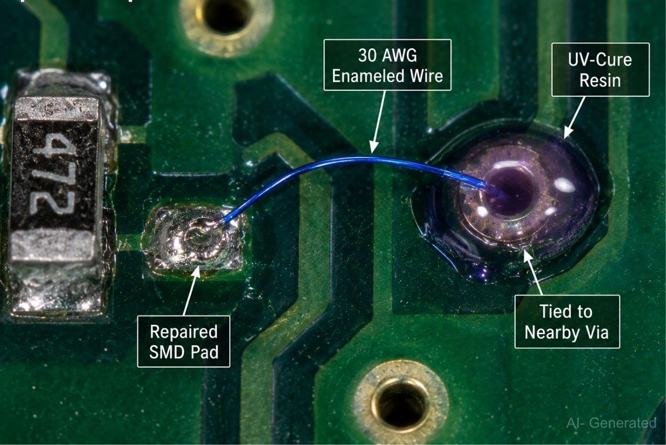
Figure: A professional PCB pad repair using a fine gauge jumper wire and UV adhesive to restore a broken connection.
SMD Rework Techniques for Common Package Types
The component's package type dictates the tools, temperature, and technique required for safe rework.
Passive Components (0201-1206)
These include chip resistors and capacitors. Their small size makes them sensitive to high airflow (they can be blown away) and asymmetric heating (leading to tombstoning). The smallest sizes, like 0201, require very fine nozzles and low flow.
SOIC/SOP Packages
These packages have leads extending from two opposite sides of the component body. Because the leads are highly visible and accessible, these packages can be reworked effectively using either a hot air station or a soldering iron, such as the drag soldering technique with a bevel or hoof tip.
QFP Packages
Quad Flat Packages (QFP) feature leads on all four sides, making them more susceptible to solder bridging compared to SOIC/SOP devices. While hot air is standard for removal, the drag soldering technique using a bevel or hoof tip with generous flux is also highly effective for installation and replacement.
QFN/DFN Packages
Quad Flat No-lead (QFN) packages lack leads and use pads hidden underneath the component body. This design prevents a standard soldering iron from reaching the joints, making a hot air station and bottom-side preheater mandatory for reliable rework.
Ball Grid Array Packages (BGA)
BGA packages utilize underside solder spheres, hiding joints from standard irons. Rework requires specialized equipment, such as closed-loop thermal profiling and split-vision optical alignment, to ensure precision. A dedicated station is mandatory for managing bottom-side preheating and controlled top-side reflow, typically followed by X-ray verification to detect hidden bridging or voids.
| Package | Difficulty | Beginner Friendly | Typical Tool |
|---|---|---|---|
| 0805 | Easy | Yes | Soldering Iron |
| 0603 | Easy | Yes | Iron/Hot Air |
| SOIC/SOP | Easy | Yes | Iron/Hot Air |
| QFP | Moderate | Some Experience | Hot Air + Preheat / Iron |
| QFN/DFN | Hard | No | Hot Air + Preheater |
| BGA | Expert | No | Dedicated BGA Rework Station |
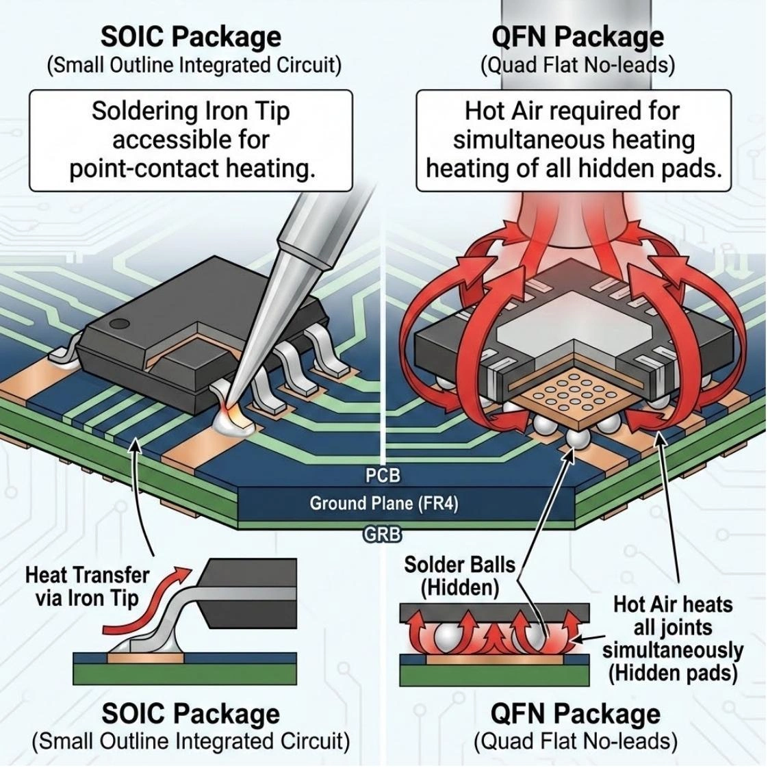
Figure: Comparing SOIC (accessible leads) and QFN (hidden thermal pad) packages, visually explaining why hot air is required for QFN rework.
Essential SMD Rework Tools
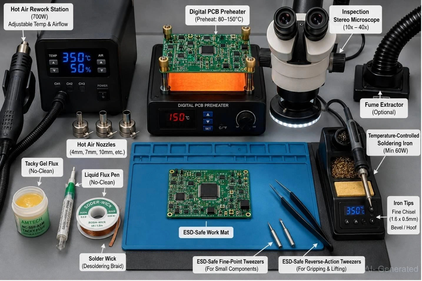
Figure: A comprehensive SMD rework bench setup, including a hot air station, soldering iron, preheater, microscope, various fluxes, solder wick, and professional tweezers.
Hot Air Rework Station
A minimum 700 W station is required to handle ground-connected thermal pads. Use three main nozzles: 4 mm jet (passives), 7–8 mm round (SOIC/QFP), and 10–12 mm (QFN/modules). The station must have adjustable airflow (1–120 L/min).
Temperature-Controlled Soldering Iron
Minimum 60 W. Essential tips include a fine chisel tip (1.6 x 0.5 mm) for general work and a hoof/bevel tip for drag soldering fine-pitch components. Uncontrolled irons should be avoided as they wander 50–100 °C.
Flux Types and Selection
Tacky no-clean gel flux is the industry default for most hot air removal and placement. Liquid no-clean pen flux is ideal for lubrication during drag soldering. Always avoid water-soluble flux unless the board can be thoroughly washed immediately, as residues are corrosive. Understanding the best flux for soldering properties is key.
Solder Wick and Desoldering Materials
Always apply flux to the solder wick braid before contact with the pads. A dry wick will surface-bond to the tinned copper and grip the pad, tearing the copper before absorbing solder.
Tweezers and Handling Tools
Essential for component handling and removal: ESD-safe fine-point tweezers for passive components and reverse-action tweezers to hold the package during hot air reflow.
Inspection Equipment
A 10x magnification loupe is the minimum requirement. For fine-pitch packages like QFP and QFN, a 10–40x stereo microscope is mandatory to verify joint quality and alignment.
PCB Preheaters
Highly recommended for multi-layer boards (four layers or more) or boards with large ground planes. A bottom-side preheat of 80–150 °C closes the thermal gap, allowing top-side hot air temperatures to remain safe for the FR-4 substrate.
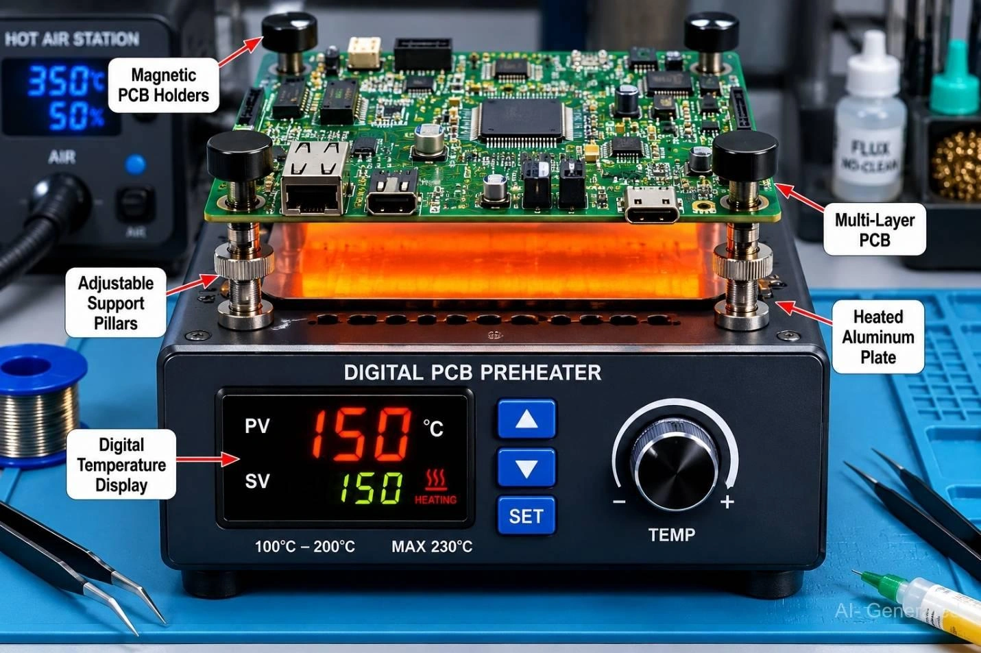
Figure: A PCB preheater warming a circuit board from below to prevent thermal stress during SMD rework.
Choosing SMD Rework Stations
For BGA packages, professional rework requires closed-loop thermal profiling systems, split-vision optical alignment, and the ability to perform X-ray verification of hidden solder joints.
Budget SMD Rework Stations
Typically priced from $40–80 (e.g., Yihua 959D, KSGER 858D). Best for hobbyists and occasional prototype rework. They offer basic functionality but often have less stable temperature control and lower-quality air pumps.
Mid-Range SMD Rework Stations
Priced from $80-150 (e.g., Quick 861DW, Atten ST-862D). These stations provide more stable temperature regulation and higher power, making them suitable for daily prototype and small-run rework.
Professional SMD Rework Stations
Priced from $400-900 (e.g., Hakko FR-702, Hakko FR-810B, Hakko FR-811, JBC JTSE). Designed for production environments, offering rapid heat-up, precise thermal stability, and fine-pitch capability.
BGA Rework Stations
Priced from $2,000+ (e.g., Hakko FR-872, ERSA IR/PL). Dedicated systems that incorporate features necessary for BGA repair, such as pre-profiling, optical alignment, and controlled bottom heating.
| Class | Example Station | Best For | Typical Price |
|---|---|---|---|
| Budget | Yihua 858D | Hobbyists | $40–80 |
| Mid-Range | Atten ST-862D | Frequent Prototype Work | $80–200 |
| Professional | Quick 861DW / JBC JTSE | Daily Engineering Use | $300–900 |
| BGA System | ERSA IR/PL | Advanced BGA Rework | $2,000+ |
Recommended SMD Rework Temperature
Leaded Solder Temperature
For Sn63/Pb37 solder (melting point 183 °C):
- Soldering Iron: 300–330 °C.
- Hot Air: 280–360 °C, adjusted by package size.
Lead-Free Solder Temperature
For SAC305 solder (solidus 217 °C, liquidus 220 °C):
- Soldering Iron: 340–370 °C (350 °C is a common default).
- Hot Air: 320–400 °C, adjusted by package size. For lead-free rework, using a bottom preheater is highly recommended for complex, high-thermal-mass components or multi-layer boards to prevent thermal stress, though it may not be necessary for smaller, simpler packages.
| Package | Iron | Hot Air |
|---|---|---|
| 0402–0805 | 330–350 °C | 280–320 °C |
| SOIC | 340–360 °C | 320–360 °C |
| QFP | 340–370 °C | 340–380 °C |
| QFN | - | 350–400 °C |
| BGA | - | 320–360 °C |
Airflow Guidelines
Start at 40–50% of the maximum airflow. High airflow can launch small components (0402/0603) and cool the air stream, lowering the actual joint temperature. For 0402 or smaller, drop to 30% airflow.
Temperature Mistakes That Damage PCBs
Heat exposure can discolor FR-4, weaken pad adhesion, and increase the risk of delamination. Temperatures above 400°C, especially when applied for extended periods without preheating, significantly increase the risk of PCB damage.
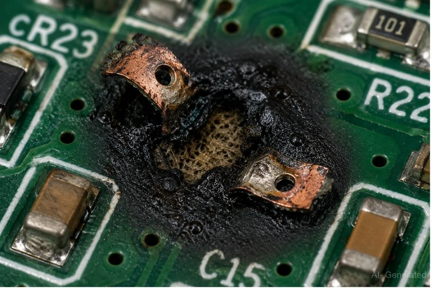
Figure: A burnt PCB substrate and lifted copper pads caused by using excessively high hot air temperatures.
How to Desolder SMD Components Without Damaging PCB Pads
Step 1 - Apply Flux
Generously apply tacky no-clean gel flux to all leads and pads of the target component. Flux is the single most important consumable; it prevents oxidation, improves thermal transfer, and allows the solder to release cleanly, preventing the joint from gripping the copper pad.
Step 2 - Preheat the PCB
For high-thermal-mass components (QFN, BGA) or multi-layer boards, activate the bottom preheater to 80–150 °C before applying top-side hot air.
Step 3 - Apply Controlled Heat
Use the lowest effective setpoint and begin small, circular sweeps over the package. Watch for the solder to transition from dull to shiny—a uniform shimmer across all joints confirms the solder is fully molten and ready for removal.
Step 4 - Remove the Component Safely
Nudge the component gently with tweezers. Never pry or apply force. If the component resists, the solder is not fully molten; add more flux, add more heat, and wait. Forcing a partially solid joint is the primary cause of tearing the pad from the substrate.
Bench Tip
The "Why It Won't Move" Rule - If a component is not moving after 20-30 seconds of hot air, do not pull harder. The solution is always: More Flux, More Heat, More Time.
Step 5 - Clean and Inspect the Pads
Flux the desoldering braid before pressing it onto the pad, then apply heat through the braid with a soldering iron. Clean the area to a flat, evenly tinned surface. Rinse with isopropyl alcohol (IPA) and inspect under magnification to ensure the pad copper is intact and no trace damage has occurred.
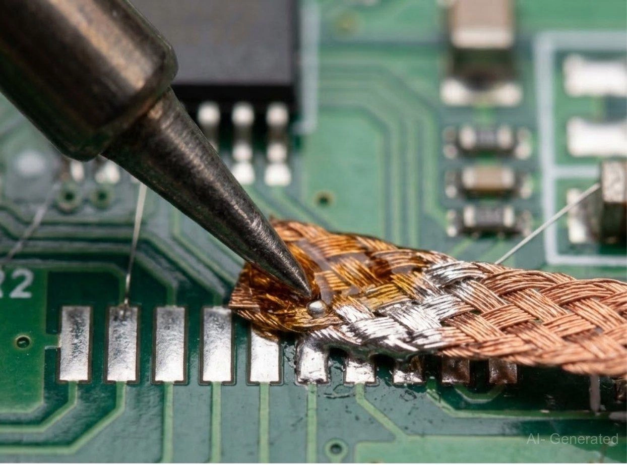
Figure: Solder wick being used to remove excess solder from PCB pads after component removal.
How to Install Replacement SMD Components
SMD Rework Checklist:
1. Verify fault
2. Apply flux
3. Preheat if required
4. Remove component
5. Clean pads
6. Install replacement
7. Inspect joints
8. Test functionality
Step 1 - Prepare Pads With Solder or Paste
For iron soldering, pre-tin all pads with a thin, flat film of solder. For hot-air reflow (QFN, BGA, modules), apply Type 4 no-clean solder paste via a syringe or mini-stencil.
Step 2 - Place and Align the Component
Align the component precisely to the silkscreen and pad outlines. For leaded packages such as SOIC and QFP, tack two diagonal corner pins with a soldering iron before proceeding. This "locks" the component in place and prevents shifting during reflow.
Step 3 - Reflow the Solder Joints
Apply the same disciplined temperature and airflow profile used for removal. For gull-wing packages, use the drag soldering technique: apply liquid flux, melt a small bead of solder onto a clean hoof tip, and swiftly drag the tip across the pins.
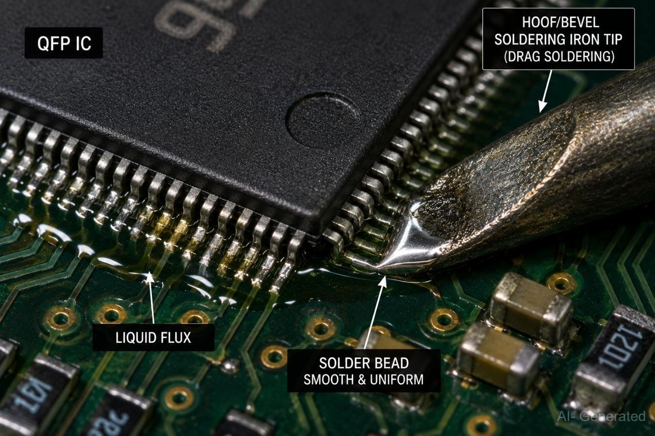
Figure: The drag soldering technique, showing a bevel iron tip passing over QFP leads lubricated with liquid flux.
Step 4 - Perform Inspection and Verification
Check every joint under magnification for smooth, concave fillets (the desired joint shape), ensuring there are no dull, balled-up joints. Follow up with continuity testing, a current-limited power-up sequence, and full functional verification.
Common SMD Rework Mistakes and How to Avoid Them
| Problem | Cause | Fix |
|---|---|---|
| Lifted Pad | Removing component before solder is fully molten | Ensure complete solder reflow before lifting |
| Solder Bridge | Excess solder or insufficient flux | Remove with flux and solder wick |
| Tombstoning | Uneven heating or solder volume | Heat both pads evenly |
| Burned PCB | Excessive temperature or dwell time | Use proper thermal profiles and preheating |
| Component Misalignment | Movement during reflow | Secure alignment before soldering |
| Cold Joint | Insufficient heat or poor wetting | Reflow with fresh flux |
| Damaged Component | ESD or overheating | Follow ESD and temperature controls |
Most Critical Mistakes to Avoid
- Pulling before solder melts
- Excessive temperature
- Excessive airflow
- Dry wick
- No flux
Hot Air vs Soldering Iron: Which Is Better for SMD Rework?
| Feature | Hot Air Station | Soldering Iron |
|---|---|---|
| Component Removal | Excellent | Good for simple packages |
| QFN Rework | Excellent | Limited |
| BGA Rework | Dedicated Equipment Required | Not Suitable |
| Touch-Up Work | Moderate | Excellent |
| Nearby Component Risk | Higher | Lower |
The accessibility of the solder joints largely determines the appropriate rework tool. Soldering irons excel at touch-up work, pad preparation, and replacing simple leaded components, while hot air stations are preferred for removing multi-pin devices and reworking packages with hidden solder joints such as QFNs. BGA packages typically require dedicated rework equipment with controlled thermal profiling.
SMD Rework vs Ordering a New PCB Assembly
Engineers must quickly compare the labor cost of rework against the procurement cost and time of a new assembly. If a board shows multiple failures, structural damage, or delamination, a new assembly from a high-quality manufacturer like JLCPCB is the better option.
High-quality EMS providers use Automated Optical Inspection (AOI), Solder Paste Inspection (SPI), and X-ray inspection in a process-controlled manufacturing environment to reduce assembly defects and improve yield consistency.
| Situation | Action |
|---|---|
| Single Failed Component | Rework |
| Wrong Resistor Value | Rework (if accessible and isolated) |
| Burned Regulator | Rework (if PCB is not thermally or electrically damaged) |
| Multiple Lifted Pads | Repair or Replace depending on severity |
| Delaminated PCB | Replace |
| Design Error | New Revision |

For prototype iterations and production-ready builds, PCB assembly services from JLCPCB allow engineers to quickly move from design to manufacturing with higher first-pass success rates, reducing the need for time-consuming rework.
FAQs on SMD Rework
Q: What is SMD rework?
SMD rework is the targeted process of removing and replacing faulty surface-mount components on an already assembled printed circuit board (PCB) using localized heat, flux, and specialized tools to restore the board's original function.
Q: What temperature should I use for lead-free SMD rework?
For lead-free SAC305 solder, set your iron between 340 °C and 370 °C. Hot air settings should typically range from 320 °C to 400 °C, adjusted according to the component size and thermal mass. Always add 80 °C to 150 °C bottom preheat for multilayer boards to prevent thermal shock.
Q: Can I perform SMD rework without hot air?
A hot air station is not strictly necessary for simple gull-wing packages (like SOIC, TSSOP, or QFP), which can be managed with a fine-tipped, temperature-controlled soldering iron and flux. However, a hot air station is mandatory for packages with hidden thermal pads, such as QFN and BGA, as the iron cannot access the solder joints.
Q: Why do PCB pads lift during rework?
Pad lifting is almost always caused by applying mechanical force (prying or pulling) before the solder is 100% molten across all joints. The partially solid solder creates a bond that tears the copper pad away from the PCB substrate (FR-4) when force is applied.
Q: Can I safely reuse an SMD component after removal?
Passive components (resistors, capacitors) often survive rework if not overheated. However, active integrated circuits (especially complex packages like QFN and BGA) should be treated as unreliable after removal, as hidden solder joint damage or thermal stress might compromise long-term function. It is recommended to use a new component from your parts inventory for final assemblies.
Q: How many times can you safely rework a PCB pad before it damages the board?
While there is no hard industry limit, repeatedly heating the same site increases cumulative thermal damage to the FR-4 and stresses the barrel of nearby vias. As a practical rule, assess the board condition carefully after the third rework cycle; subsequent attempts carry a high risk of permanent damage and reduced reliability.
Conclusion
A successful SMD rework job rarely looks dramatic. The component comes off cleanly. The pads stay intact. The replacement works on the first power-up. Getting there is usually the result of three habits: plenty of flux, controlled heat, and zero mechanical force.
Those same habits apply whether you're replacing a wrong-value resistor on a prototype or reworking a QFN package on a multilayer board. Use rework when it saves time. Replace the board when damage becomes structural. Knowing the difference is what separates efficient troubleshooting from wasted effort.
Popular Articles
• Common PCB Assembly Methods and Soldering Techniques Explained
• What Is BGA Void? Causes, IPC Limits, and Solutions
• SMD Soldering Tools You Need: Complete Guide from Beginner to Pro
• Reflow Soldering: Everything You Need to Know
• SMT Assembly Process Explained and Equipment Used: A Step-by-Step Guide to PCBA Manufacturing
Keep Learning
Common PCB Assembly Methods and Soldering Techniques Explained
Whether you're designing your first prototype or scaling up to production, understanding PCB assembly methods and soldering techniques is crucial to achieving reliable, high-performance circuit boards. Modern PCBA primarily relies on Surface Mount Technology (SMT) and Through-Hole Technology (THT)—each offering unique advantages for component density, durability, and manufacturability. In this guide, we'll break down the major PCB assembly methods, key soldering techniques such as reflow and wave sold......
12 Professional Soldering Tips and Tricks Every Beginner Should Know
Soldering is not merely "gluing" metal; it is a metallurgical process that creates an intermetallic compound (IMC). This molecular bond ensures the electrical and mechanical integrity of your device. A poor joint might pass a quick visual check but will inevitably fail under vibration or thermal stress, leading to "ghost" bugs and hardware failures. These soldering tips and tricks focus on practical, repeatable techniques used in professional electronics soldering—from correct heat transfer and flux u......
Solder Melting Point Guide: Chart, Alloy Types, and Reflow Considerations
In the precise world of electronics manufacturing, a difference of just a few degrees can mean the distinction between a perfect, reliable solder joint and a catastrophic "cold" joint failure. While many hobbyists view soldering simply as "melting metal to stick things together," professional PCB assembly requires a nuanced understanding of thermodynamics. The solder melting point is not simply a single value listed in a datasheet; it is a decisive limit that determines the choice of components, the s......
The Ultimate Guide to Solder Flux: Everything You Should Know Before Soldering PCB
Soldering is needed to make almost all electronic devices. Adding solder alone won't make a joint that is strong, clean, and sound from a metallurgical point of view. Solder flux is a very important part of the process that comes in here. If you want to do your job better and make it more reliable, you need to know a lot about soldering flux, whether you're an engineer, a professional technician, or just a hobbyist. This article goes into a lot of detail about solder flux, including what it is, how it......
Flex PCB Assembly Guide: Process, Challenges, and Solutions
Flexible Printed Circuit Boards (Flex PCBs) are the foundational technology enabling the compact, innovative design of modern electronics. Because of their ability to bend and fold, they power devices from smart wearables to compact medical instruments where traditional rigid printed circuit boards (Rigid PCBs) can't be used. Achieving a functional electronic circuit from the raw plastic film demands special expertise, with flexible PCB assembly (FPCA) representing the crucial final step in this trans......
SMD Rework Guide: Tools, Temperatures, and Techniques That Prevent PCB Damage
From replacing a burned regulator to correcting wrong component values or removing solder bridges on fine-pitch ICs, SMD rework is an essential skill in electronics manufacturing and prototyping. It allows engineers to repair assembly defects, implement design changes, and recover valuable PCBs without the cost and delay of building new boards. In this guide, you will learn: What SMD rework is Common rework scenarios Tools and temperatures Safe removal and installation Package-specific techniques Real......