Stacked or Staggered Vias? Choosing the Best Option for Reliable HDI PCBs
15 min
- Understanding Stacked and Staggered Vias
- Key Advantages of Staggered Vias in HDI Manufacturing
- Design Considerations When Choosing Via Types
- Manufacturing Challenges and Professional Solutions
- JLCPCB's Expertise in Staggered Via HDI Production
- FAQ about Staggered Via
- Conclusion:
Key Takeaways
- Structures: Stacked vias align vertically (need copper fill); staggered vias are offset laterally.
- Reliability: Staggered vias better resist thermal stress across 3+ layers.
- Cost & Yield: Staggered vias cut manufacturing steps, raising yield and saving cost.
- Space: Stacked vias fit tight, fine-pitch BGA breakouts best.
- Decision: Choose stacked for extreme density, staggered for reliable savings.
Ever since taking a closer look at the guts of a smartphone motherboard, you may have thought: How do all these connections fit in such a small area? The magic lies in the microvias, minuscule holes drilled by a laser that connect layers. And once you begin stacking those microvias on top of each other on multiple build-up layers, you come to a fork in the road: staggered via or stacked via! This is a seemingly insignificant decision, but it has a direct impact on reliability, yield, and cost. Get it right, and your HDI board successfully passes thermal cycling and volume production without a problem.
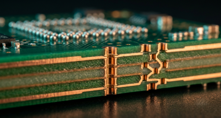
If you get it wrong, you might end up looking for intermittent failures that reveal themselves after reflow and/or field aging. In this guide, we will dissect the stacked and staggered vias from the bottom up: the geometry, the trade-offs, and the design rules that divide the two. In conclusion, you'll be able to identify when to use staggered vias and when stacked vias can be beneficial, and how a reliable manufacturer such as JLCPCB can make either option a reliable board.
Understanding Stacked and Staggered Vias
Let's anchor the two structures before comparing. They are both part of the world of HDI (High-Density Interconnect) boards, where laser-drilled microvias are used instead of bulky, mechanical through-holes to link adjacent copper layers. The difference is only the way you lay out those microvias if you have to go through more than one dielectric layer.
What Staggered Vias Are and How They Differ from Stacked Vias
Microvia is a small blind via generally smaller than 0.15mm, which is used for an HDI build-up to connect one layer to the next one. If your signal requires crossing just one layer, then one microvia is enough. The trouble is when you have to cross two or more layers.
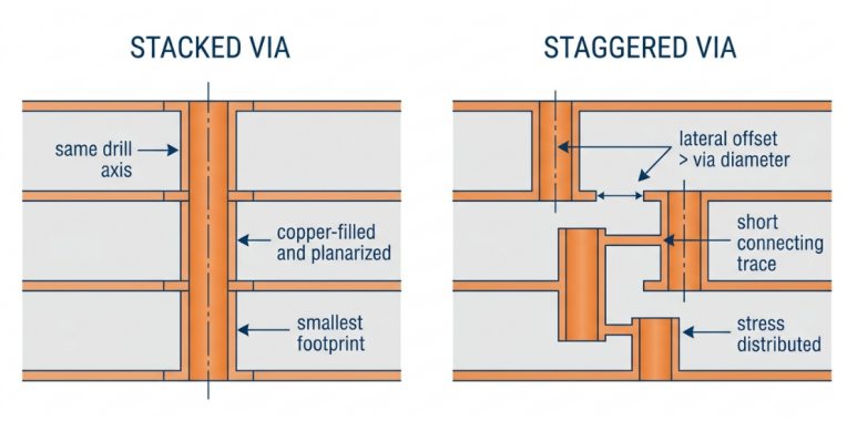
A stacked via is a microvia in a column, with microvias stacked vertically on top of one another, sharing the same vertical axis like coins in a stack. The way this is accomplished is by electroplating copper into each microvia and planarizing (flattening) it before the next microvia lands. The stacked structure itself would be unreliable and dimpled if it did not have the copper filling.
In contrast, a staggered via is offset laterally on successive layers and connected by a short trace on the common layer. The existing path follows a minor ‘zigzag' rather than a straight up-and-down path. The important rule of thumb is that the distance between the two should be greater than the diameter of the microvia; that is, the center-to-center distance between the two holes should be greater than the microvia hole so that the two holes never overlap or interfere with one another during the laser drilling and plating process.
Common Use Cases in High-Density Interconnect Designs
Stacked and staggered vias are found wherever board space is valuable, and the number of layers increases. Both structures allow designers to break away from the constraints of fine pitch parts, which mechanical vias cannot support.
- Fine-pitch BGAs and CSPs: 0.4 mm and 0.5 mm pitch packages require microvias to escape from the inner rows, and to not starve the routing channels.
- Ultra-thin builds: On smartphones and wearables, the overall stack is reduced by utilizing stacked or staggered microvias, ensuring that all of the nets remain connected.
- Microvia is employed in high-speed digital: DDR, PCIe, and RF Front Ends – to reduce stub length and minimize current loops to improve signal integrity.
- Automotive and industrial modules: In these applications, reliability under temperature swings is most important, and this is often what decides in favor of staggering the vias.
In reality, staggered vias are the default workhorse for many HDI stacks, and stacked vias are used when the breakout area is so dense that you just can't afford the lateral offset of a staggered via.
Key Advantages of Staggered Vias in HDI Manufacturing
So why is it that many experienced HDI designers opt for staggered vias when the layout will support it? It depends on 2 key factors that engineers are very interested in: reliability and yield.
Improved Reliability and Reduced Thermal Stress
All PCBs carry a constant tension with them, known as CTE (Coefficient of Thermal Expansion) mismatch. The dielectric resin has a thermal expansion coefficient considerably higher than that of the copper resin, of the order of 200 ppm/°C for the Z-axis resin compared to around 16–17 ppm/°C for copper. Stresses on the via structure are incurred during every reflow cycle and with each power-up in the field.
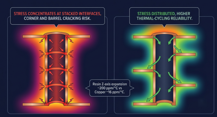
That stress is focused at the interfaces between one copper-filled microvia and the next in a stacked via. After stacking three or more layers, the strain may become too great at the corners, causing it to crack or separate the barrel from the corner. The higher the column, the more concentrated the load becomes at one line of force. Stressed vias are staggered to ensure the even distribution of that stress. No single interface is subject to the entire Z-axis load since each microvia is mounted on a separate landing pad and is connected by a short trace. The zig-zag geometry provides space to flex, which is the reason staggered vias tend to perform better than tall stacked columns during thermal cycling tests. That mechanical margin is significant for any product that is going to experience a large range of temperatures.
Higher Manufacturing Yield Compared to Stacked Configurations
Apart from reliability, staggered vias are just easier to manufacture. This is a very demanding sequential process: laser drill, copper-fill plate, planarize flat, image, and repeat all of the above for the next layer. Each of those extra steps is a chance for a defect. There are several factors that can cause a stacked column to fail, including voids in the copper fill, dishing during planarization, or a fraction of a mil of misalignment. Staggered vias eliminate the need for the required fill-and-planarize loop on inner interfaces, reduce process steps, and reduce potential failure points. Fewer plating/planarization cycles result in less opportunity for voiding and dishing defects.
- Loose registration: As the offset holes don't have to be directly in the middle of the pad below them.
- Lower cost per board: No repeated copper fill plating of each stacked interface.
- Quicker turnaround for fabrication as the sequence of building is shorter and simpler.
The end effect is a more productive process, which keeps unit cost down, a significant advantage when you go from prototype to volume.
Design Considerations When Choosing Via Types
All this does NOT imply staggered vias are always the winner. Depending on the number of layers, the density, and the sensitivity of your signals, you will be able to choose the right one. Let's examine the factors that should be the determining ones.
Aspect Ratio, Layer Count, and Signal Integrity Impact
The ratio of via depth to diameter, aspect ratio (AR), is the first number to check. IPC guidance is to keep the aspect ratio at or below about 1:1 for a single layer of microvia, as the reliability of copper plating decreases as the hole becomes deeper relative to its diameter. This is one of the reasons why IPC warns against high stacks: stacking exacerbates the challenge layer by layer.
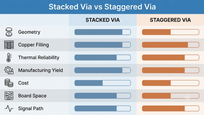
The number of layers is just as important. Two layers of transition are fine either way, but at three or four layers of build-up, it's a matter of making a reliability gamble with a stacked column or keeping it easy with a staggered column. The counterweight is signal integrity. A stacked via provides a clean and uniform vertical path, facilitating controlled impedance on the fastest nets. A staggered via adds a slight offset and a small trace length for a slight impedance mismatch. This is not a huge impact for most designs, but for multi-gigabit lanes where every picosecond counts, it can be an issue. Now, here are the comparisons of the two structures with respect to the factors that determine a design:
| Factor | Stacked Via | Staggered Via |
|---|---|---|
| Geometry | Microvias aligned on one vertical axis | Microvias offset laterally, linked by short traces |
| Copper filling requirement | Mandatory on every inner via | Only where via meets an outer layer |
| Reliability under thermal cycling | Lower for 3+ layers (stress concentrates) | Higher (stress distributed) |
| Manufacturing yield | Lower (fill, planarize, tight registration) | Higher (fewer critical steps) |
| Relative cost | Higher | Lower |
| Board space used | Minimal (smallest footprint) | Slightly larger (needs offset room) |
| Signalpath/impedancee | Uniform, best for ultra-high-speed | Minor discontinuity from offset |
When Staggered Vias Provide Clear Benefits Over Stacked Vias
As you can see from the table, a practical decision rule becomes apparent. Consider using staggered vias for designs that are much more about reliability, cost, and yield than about the smallest possible footprint.
- You're putting three or more build-up layers on, and you're likely to have cracking problems at the top of the stack of tall columns.
- Your product is subjected to severe thermal cycling, such as automotive, industrial, or outdoor equipment.
- There is some lateral clearance with the common layer to line up the holes without spacing problems.
- The concern is cost and yield with a volume build; you do not want to have to repeat the copper-fill plating.
- You have medium speed signals, and a slight impedance discontinuity is not a problem.
If the smallest possible footprint is required under a dense fine-pitch BGA, or if a perfectly even "vertical" path is needed for ultra-high-speed nets, consider stacked vias, but be prepared to pay more and accept more process control challenges.
Manufacturing Challenges and Professional Solutions
No matter which structure you choose, the fabricator must be able to produce it to perfection. Here is where you'll notice the difference between an HDI line and a hobby-grade shop.
Precision Alignment and Plating for Staggered Structures
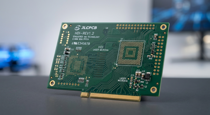
While staggered vias are less complex than stacked columns, "less complex" is relative. Laser drilling still needs to precisely hit the correct landing pad, and layer-to-layer registration needs to have a very small tolerance in order to ensure that the offset microvia lands correctly on the target trace. The plating process is also challenging. A microvia that is not entirely copper-filled,d even if blind, should have a uniform copper plating without voids on the sides to ensure a solid connection. Insufficient throwing power in the plating bath results in an inadequate amount of metal on the bottom of the via, a common cause of open circuits after thermal stress. This coverage is maintained even by controlling the electroplating chemistry and current density.
Advanced Processes to Ensure Via Reliability
It's higher still for stacked vias. The copper-fill plating needs to form a dense, void-free plug, while planarization needs to keep a surface flat to within microns to provide a true base for the next microvia. Any dishing or trapped void makes a weak point, which thermal cycling will eventually take advantage of.
Several process controls are essential to maintaining the reliability of both structures, and are used by professional fabricators:
- Sequential lamination with very close registration between successive build-up operations.
- Plating with void-free copper with optimized bath chemistry for stacked structures.
- Precision planarization of filled vias (flattening to the next layer).
- Quality control checks on microsection and X-ray inspection to ensure correct fill and alignment prior to shipping.
- Thermal cycling and Interconnect Stress Test (IST) validation for long-term durability.
These are the steps that take a nifty stackup concept from paper to a board that will last for years in the field.
JLCPCB's Expertise in Staggered Via HDI Production
It's easy to know the theory, but it's hard to find someone who can do it over and over again. Whether your design is based upon staggered vias, stacked vias, or a combination of both, this is where JLCPCB's HDI capabilities come into play.
Advanced HDI Capabilities for Complex Via Arrangements
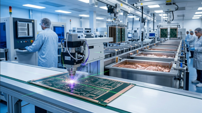
JLCPCB operates a modern HDI line that is based on laser-drilled microvia staggering and stacking down to 0.15 mm. There are standard build-ups like 1+N+1 and 2+N+2 that encompass 99.9% of fine-pitch BGA and mobile-class designs, and provide the layer transitions necessary to break out dense components. In the stacked configuration, JLCPCB provides copper via filling, which is a kind of electroplated planarized fill absolutely required by a reliable stacked column. This is because you do not have to design around the process restrictions: you can simply state the arrangement you need for your signal and density budget.
DFM Support and High-Yield Fabrication
A second set of eyes is helpful for any great process before fabrication. JLCPCB's DFM (Design for Manufacturability) checks will indicate a problem, such as too little via offset, too aggressive aspect ratios, or registration risks, at the quote stage, not after receiving a failed batch. This feedback loop can help you make rapid iterations while maintaining high yields, along with an instantaneous online quoting system and a quick turnaround. High yield isn't only a cost story, it's a reliability story too, since a process that can be repeated time and time again is the one that will give you a stable and repeatable yield of consistent vias board after board.
Proven Reliability from Prototype to Volume Production
The true litmus test of any via-based strategy is if it scales. A structure that functions well on a few prototypes, but which floats during mass production, is a trap. With JLCPCB's controlled HDI process, you will obtain the same via reliability from your initial prototype all the way to full production. That consistency, coupled with inspection techniques such as X-ray and electrical testing, allows you to be confident in your design. Staggered vias for thermal margin or stacked vias for footprint, you can choose and get a fabrication partner who can provide it reliably, and at a price that makes HDI affordable.
FAQ about Staggered Via
Q: What is a staggered via, in simple terms?
A staggered via is a set of HDI microvias placed on adjacent layers but offset laterally instead of aligned in a column, connected by a short trace on the shared layer. This zig-zag path spreads thermal stress and avoids the mandatory copper-fill-and-planarize steps that stacked vias require.
Q: What is the main difference in the stacked via vs staggered via decision?
Stacked vias share one vertical axis for the smallest footprint and cleanest signal path, but every inner via must be copper-filled and planarized. Staggered vias trade a little board space for higher reliability, easier fabrication, and lower cost.
Q:Do stacked and staggered vias both need copper filling?
Stacked vias require electroplated copper filling on every inner via, so the next microvia has a solid, flat base. Staggered vias only need filling where a via connects to an outer layer, which is one reason they are cheaper and higher-yield.
Q: Are staggered vias more reliable than stacked vias?
For transitions spanning three or more layers, yes. Staggered vias distribute CTE-driven thermal stress instead of concentrating it at stacked interfaces, so they typically survive thermal cycling better. For two-layer transitions, both perform well.
Q: Can I get staggered and stacked via HDI boards from JLCPCB?
Yes. JLCPCB's HDI line supports laser microvias down to 0.15 mm, 1+N+1 and 2+N+2 build-ups, and copper via filling for stacked structures, all backed by DFM review and reliability testing. Upload your design for an instant quote and let their engineers help you land the right via strategy from prototype to volume.
Conclusion:
It's not just a matter of either-or. It is a compromise between density, reliability, and cost: staggered vs stacked vias. The staggered via becomes the workhorse default for most HDI designs, as it has been shown to provide better thermal robusticity, improved manufacturing yield, and reduced costs, particularly for three or more build-up layers. Use stacked vias only in the breakout areas where the footprint absolutely cannot be reduced. In the end, having it correct on paper is not enough if the fabricator doesn't have the ability to make it perfect. A professional HDI partner such as JLCPCB fills this gap and makes your via strategy a reality in your consistently flawless boards from prototype to volume production. The result is a design that is thermal cycle resistant and has high reliability.

Keep Learning
Is FR4 the Best Board Material for Your Design
Key Takeaways Best All-Rounder: Ideal balance of strength, insulation, and low cost for standard PCBs. Clear Limits: Poor heat dissipation (~0.3 W/m·K) and high loss for RF (>3 GHz). Alternatives: Use Rogers for RF, Aluminum for high heat, and FPC for flexibility. Selection Essentials: Pick High-Tg (170°C+) for lead-free reflow and custom stackups for impedance. JLCPCB Advantage: 1–32 layer FR4 boards with ±10% impedance control and 24h fast dispatch. In the world of electronics and printed circuit bo......
Optimizing High-Voltage Circuit Safety with PCB Dielectric Strength
Key Takeaways Non-linear Scaling: Dielectric strength drops as thickness increases. Safety vs Signals: Dielectric strength ensures safety, while Dk controls signal speed. Material Selection: High-voltage safety depends on Tg, CTI, and moisture resistance. Spacing Rules: Clearance prevents air arcs, while creepage prevents surface tracking. Assembly Testing: Hi-pot testing requires finished assemblies, not bare boards. Dielectric strength is the number engineers quote to prove a board is safe at mains ......
How Copper Foil Shapes PCB Performance and Manufacturing Quality
Key Takeaways Weight: 1 oz copper ≈ 35 µm thickness; higher weight increases current capacity. Types: ED for standard rigid boards, RA for dynamic flex circuits. DFM & Loss: Smoother foil lowers RF loss; thicker foil requires wider trace spacing. The part of a PCB that actually carries the electrical signal is the copper foil. The strength comes from the glass weave, the resin is used to keep the layers together, and the solder mask is used to provide protection and separation of exposed copper. But w......
A Complete Guide to Copper Clad Laminate (CCL) in PCB Manufacturing
Key Takeaways CCL is the base material: a cured resin-reinforcement sheet with copper foil bonded to one or both sides. Three parts control performance: Resin affects heat and loss, reinforcement controls stability, and copper foil affects conductor behavior. Choose by the main design stress: Heat, frequency, and cost usually determine the best laminate family. Slash sheets define the material: IPC-4101 uses numbered slash sheets to specify rigid PCB base materials. Tg alone is not enough: Td and time......
Buried Vias in Advanced PCBs: Enabling Higher Density, Better Signal Integrity, and Compact Designs
Key Takeaways Hidden Routing: Buried vias connect only inner layers, keeping outer surfaces clear for dense components and traces. Better Signal Integrity: They eliminate via stubs, reducing parasitics and signal loss in high-speed designs. Higher Density: Essential for HDI boards, dense BGAs, and small form factors like wearables. Higher Cost: Sequential lamination and extra drilling steps make them ~3×-4× more expensive than standard through-holes. Ever wondered how a modern smartphone mainboard can......
Unlocking Higher Density and Better Performance with Blind Vias in HDI PCBs
Key Takeaway Higher Density: Connects surface to inner layers without penetrating the whole board, freeing routing channels under fine-pitch BGAs. Improved Signal Integrity: Reduces via stub length to minimize impedance discontinuities in high-speed designs. Aspect Ratio Rule: Keep the depth-to-diameter ratio near 0.75:1 (max 1:1) for reliable laser drilling and void-free plating. Thermal Efficiency: Supports via-in-pad setups for better heat dissipation and compact component placement. Ever wonder ho......