
Via Filling Explained: Key Techniques, Benefits, and Solutions for High-Performance PCBs
11 min
- What Is Via Filling and Its Role in PCB Design
- Exploring Different Types of Via Filling
- The Detailed Via Filling Process in Professional PCB Fabrication
- Major Benefits of Implementing Via Filling in Your PCBs
- Real-World Applications of Via Filling Across Industries
- JLCPCB’s Advanced Via Filling Capabilities: Demonstrating Professional Manufacturing Excellence
- FAQ
- Conclusion
Key Takeaways
Via filling completely fills plated through-holes and microvias with epoxy or conductive copper paste, followed by planarization and copper capping (POFV). It eliminates voids, solder wicking, and thermal/mechanical issues while enabling reliable via-in-pad designs. Benefits include superior heat dissipation (up to 8 W/m·K), better signal integrity, higher mechanical strength, and improved assembly yields. JLCPCB provides free non-conductive filling + POFV on 6+ layer boards. Ideal for HDI, high-power, and high-speed PCBs with vias ≤0.5 mm.
Via filling has become a cornerstone of reliable PCB fabrication as designs push toward higher layer counts, finer pitches, and greater power densities. Empty vias in multilayer boards create vulnerabilities — trapped air and flux residues during assembly, impedance discontinuities in high-speed signals, and thermal bottlenecks under power components.
By filling the via barrel completely after initial copper plating, engineers create a solid, planar structure that eliminates these risks while enabling advanced features like via-in-pad (VIP) routing. This guide explains the core techniques, material options, manufacturing steps, quantifiable benefits, real-world applications, and best practices for via filling. All details align with established professional fabrication standards, including those practiced at leading manufacturers like JLCPCB.
What Is Via Filling and Its Role in PCB Design
Definition and Basic Principles
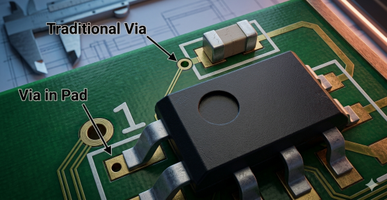
Via filling is the process of completely occupying a drilled and plated through-hole or blind via with a specialized material — either non-conductive epoxy resin or conductive copper-epoxy paste — after the initial electroless and electrolytic copper plating of the via walls. The filled via is then planarized and capped with additional copper plating to restore a flat pad surface suitable for component mounting or routing.
This process transforms a hollow copper barrel into a reinforced, void-free column. It addresses coefficient of thermal expansion (CTE) mismatches between copper (approximately 17 ppm/°C) and FR-4 substrate (12–16 ppm/°C), preventing barrel cracking during thermal cycling. In HDI designs, filled vias also support stacked microvias by reducing stress concentrations at the via knees. Fabricators recommend finished via diameters ≤0.5 mm for reliable filling, with aspect ratios kept at 1:1 or lower for microvias (laser-drilled 80–150 μm) to ensure complete fill without voids.
Via Filling vs. Via Plugging: Key Differences
Via filling and via plugging serve different purposes.
· Via Plugging uses solder mask ink or partial epoxy to seal only the via openings, leaving most of the barrel hollow. It offers basic contamination protection but limited planarity and minimal structural reinforcement.
· Via Filling completely occupies the barrel with epoxy or copper paste. After leveling, a copper cap (POFV) is added, creating a flat, solderable surface ideal for via-in-pad.
JLCPCB clearly differentiates the two: plugged vias rely on ink sealing, while filled vias deliver full barrel occupation, surface leveling within 50 μm, and a secondary copper cap (minimum 5 μm, up to 25 μm in POFV). Choose plugging for cost-sensitive designs and filling for high-reliability applications.
Exploring Different Types of Via Filling
Conductive Via Filling for Superior Electrical and Thermal Performance
Conductive via filling uses copper-epoxy paste to occupy the via barrel after wall plating. Following curing and planarization, a final copper cap is applied. This creates a continuous low-resistance path with thermal conductivity of 8 W/m·K — more than 25 times higher than air-filled vias.
Engineers select this type for power delivery networks, high-current ICs, and high-speed signals requiring reduced inductance. Optimal thermal via arrays use 0.2–0.3 mm diameter with 0.8 mm spacing. JLCPCB’s copper-paste option resists cracking under thermal cycling and works well for via-in-pad on power pads.
Non-Conductive Via Filling for Insulation and Planarity
Non-conductive filling uses standard epoxy resin to fill the via completely, followed by leveling and copper over-plating. This prioritizes mechanical reinforcement and surface flatness without adding conductivity.JLCPCB provides free non-conductive resin filling on all 6-layer and higher boards. Key advantages include:
· Depression/protrusion controlled to ≤50 μm
· Prevention of solder wicking during reflow
· Elimination of flux residue entrapment
The flat capped surface ensures reliable SMT yields for fine-pitch BGAs and QFNs.
Specialized Filling Materials and Advanced Methods
Material choice depends on the via’s function:
· Copper-epoxy paste for dual electrical/thermal performance
· Standard epoxy resin for pure insulation and cost-effectiveness
For laser-drilled microvias (80–100 μm, aspect ratio ≤1:1), pulsed electrolytic plating or copper-epoxy fill prevents voids in stacked configurations. Advanced methods include pressure-assisted dispensing under vacuum and controlled thermal curing. JLCPCB enforces strict diameter limits (≤0.5 mm) and performs AOI plus cross-section verification for >95% opacity and void-free barrels, ensuring IPC-4761 Type VII compliance. 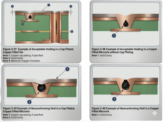
The Detailed Via Filling Process in Professional PCB Fabrication
Initial Drilling, Plating, and Via Preparation
The process starts with precision drilling — mechanical for standard holes and laser for microvias. Desmearing removes debris for strong copper adhesion. Electroless copper plating establishes a 1–2 μm seed layer, followed by electrolytic plating to achieve minimum 25 μm wall thickness. Surface copper is built to ≥5 μm for capping. Uniform deposition is essential to avoid barrel cracks under thermal stress.
Material Application and Precision Filling Techniques
Designers specify fill requirements in Gerber notes. Non-conductive epoxy or conductive copper paste is applied via screen printing or vacuum-assisted dispensing. Vacuum ensures complete penetration without air pockets. For 6+ layer boards, JLCPCB applies free resin filling as standard. Excess material is removed before curing to create a level base for via-in-pad designs.
Curing, Planarization, and Final Quality Checks
Filled vias undergo thermal curing to polymerize the resin and eliminate solvents. Automated planarization levels the surface to <50 μm variation. A second copper plating creates the POFV cap (up to 25 μm). Final inspection includes AOI, cross-section sampling, and electrical testing. JLCPCB verifies fill completeness, yellowing rate <5%, and absence of cracks to meet IPC Class 2 or 3 standards.
Table 1: Via Filling Process Steps (Typical Professional Flow)
| Step | Description | Key Controls | JLCPCB Capability |
|---|---|---|---|
| Drilling & Desmear | Create precise holes; remove residues | Aspect ratio ≤1:1 for microvias | Laser + mechanical |
| Wall Plating | Electroless/electrolytic copper | ≥5 μm surface thickness | Standard + advanced baths |
| Material Fill | Dispense epoxy or copper-epoxy | Vacuum to eliminate voids | Free resin fill on 6+ layers |
| Cure & Planarize | Thermal cure + surface leveling | Depression/protrusion ≤50 μm | Automated planarization |
| Over-Plate & Cap | Copper cap for VIP/POFV | Flat pad surface | Free POFV on 6–20 layers |
| Inspection | AOI + cross-section | Void-free, >95% opacity | IPC-aligned quality metrics |
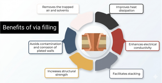
Major Benefits of Implementing Via Filling in Your PCBs
Enhanced Thermal Management and Heat Dissipation
Filled vias create efficient vertical heat pathways. Copper-paste types deliver 8 W/m·K thermal conductivity, enabling thermal via arrays (0.3 mm diameter, 0.8 mm pitch) to reduce junction temperatures by 10–20°C in power ICs. Even non-conductive fills improve heat spreading by removing air pockets that act as thermal insulators.
Improved Signal Integrity and Electrical Performance
Solid filled vias minimize inductance and impedance discontinuities in signals above 10 GHz. Conductive fills shorten current return paths in BGA packages (up to 30% lower parasitic inductance), while non-conductive fills prevent solder-induced shorts and maintain clean routing channels.
Increased Mechanical Strength and Long-Term Reliability
Filling eliminates trapped air, flux, or chemicals that expand during reflow or thermal cycling. This results in 30–50% higher pad pull strength, significantly better resistance to mechanical shock and vibration, and assembly yields exceeding 98% in via-in-pad designs with consistent solder joint volume.
Table 2: Quantitative Benefits of Via Filling (Industry & JLCPCB-Aligned Data)
| Benefit | Unfilled Via | Filled Via (Typical) | Improvement |
|---|---|---|---|
| Thermal Conductivity (copper-epoxy) | ~0.3 W/m·K (air) | 8 W/m·K | >25× better heat transfer |
| Solder Wicking Risk | High (voids common) | Eliminated | >98% assembly yield gain |
| Via Diameter Limit for Reliability | >0.5 mm risk bubbles | ≤0.5 mm standard | Consistent planarity |
| Mechanical Strength (pad pull) | Baseline | +30–50% (filled structure) | Reduced fracture risk |
| Signal Path Inductance (high-speed) | Higher discontinuities | Reduced path length | Improved SI for >10 GHz |
Real-World Applications of Via Filling Across Industries
High-Density Interconnect (HDI) PCBs in Consumer Electronics
Consumer devices such as smartphones, wearables, and 5G modules demand stacked microvias and via-in-pad filling to achieve compact footprints. Filled vias enable BGA fanout at pitches as fine as 0.4 mm while maintaining signal integrity for RF and high-speed digital interfaces. The planar surface supports direct component placement, shortening trace lengths and reducing EMI.
Demanding Environments in Automotive, Aerospace, and Medical Devices
Automotive radar modules, avionics, and medical imaging systems operate under extreme vibration, thermal shock (−40°C to +125°C), and humidity. Copper-filled thermal vias efficiently dissipate heat from power electronics, while epoxy-filled VIPs guarantee solder joint integrity in safety-critical systems. These applications leverage the mechanical reinforcement and void-free construction to meet stringent reliability standards like AEC-Q100 or IPC Class 3.Common Challenges in Via Filling and Professional Solutions
Potential Manufacturing Issues and How to Prevent Them
Common pitfalls include voids from incomplete material flow (especially in vias >0.5 mm), bubble formation during dispensing, and uneven planarity that causes SMT defects. Larger vias risk incomplete filling; excessive paste can cause surface dimples. JLCPCB mitigates these through diameter limits (≤0.5 mm), vacuum-assisted processes, and free resin filling on multilayer boards. Early DFM review catches incompatible aspect ratios or stack-up issues.
Best Practices for Flawless Execution
Clearly annotate fill requirements in fabrication notes, specifying conductive vs. non-conductive based on thermal or insulation needs. Collaborate with the fabricator during design review to validate via sizes, annular rings (minimum 0.1 mm for VIP), and clearances. Prototype with cross-section analysis to verify fill quality before production. Choose POFV for via-in-pad to ensure flatness and reliability. These steps, combined with traceable processes and IPC-aligned inspection, deliver consistent, high-yield results.
JLCPCB’s Advanced Via Filling Capabilities: Demonstrating Professional Manufacturing Excellence
JLCPCB has integrated via filling into its core fabrication platform with notable efficiency. For 6-layer and higher boards, non-conductive resin filling is provided at no extra cost, and POFV (plated over filled via) is the free default for via-in-pad on 6–20 layer orders. Copper-paste-filled vias deliver the documented 8 W/m·K thermal conductivity with surface copper caps of ≥5 μm (up to 25 μm in advanced POFV).
State-of-the-art dispensing equipment, pulsed plating, and automated planarization guarantee void-free fills even in dense HDI microvia stacks. Quality assurance follows traceable, IPC-aligned workflows: AOI, electrical testing, and sample cross-sections confirm fill completeness, flatness, and performance. Engineers receive detailed DFM feedback, rapid prototyping turnaround, and full technical support for custom specifications—whether thermal vias under processors or dense BGA routing. These capabilities reduce total cost of ownership while accelerating time-to-market for complex, high-performance designs.
FAQ
Q: What is the main difference between via filling and via plugging?
Via filling completely fills the barrel with epoxy or copper paste and adds a flat copper cap. Via plugging only seals the openings with solder mask or partial fill, leaving the barrel mostly hollow.
Q: When should I choose conductive via filling?
Choose conductive (copper-epoxy) filling when you need excellent thermal conductivity (8 W/m·K) and low electrical resistance, such as under power ICs or in high-current paths.
Q: What is the maximum recommended via diameter for filling?
JLCPCB recommends ≤0.5 mm finished diameter for reliable filling. Larger vias increase the risk of voids and incomplete fill.
Q: Does JLCPCB offer free via filling?
Yes. Non-conductive resin filling and POFV (plated over filled via) are free on all 6-layer and higher boards.
Q: What are the biggest benefits of via-in-pad with filling?
It enables finer BGA pitches, prevents solder wicking, improves planarity (≤50 μm), and significantly increases assembly yield and reliability.
Q: How do I specify via filling in my design?
Clearly note the via type (conductive or non-conductive), locations, and requirements in Gerber files or fabrication notes. Early DFM review with the manufacturer is highly recommended.
Conclusion
Via filling is now essential for high-performance PCBs, solving thermal, electrical, and mechanical challenges in one step. By understanding these techniques and benefits, designers can specify filled vias with confidence. Partnering with JLCPCB — with its free advanced filling options and proven quality systems — ensures reliable results. Review your next design and incorporate via filling where it adds value.
Keep Learning
How Beveled Edges Improve Reliability and Performance in Card Edge Connectors
Key Takeaways Beveled edges enable smooth insertion and protect gold fingers from wear in card edge connectors. Use 30° or 45° angles (45° is standard for most designs) with depth of 1/3 to 1/2 board thickness. They reduce insertion force, prevent plating damage, and improve long-term contact reliability. Proper beveling is critical for high-cycle applications like DDR modules and PCIe cards. Bevel edges came into my attention the first time a memory module that I designed scratched its own gold finge......
How to Prepare Perfect Gerber Files for Flawless PCB Production
Key Takeaways Use RS-274X format and consistent millimeter units for all files. Always include complete layers: Copper, Solder Mask, Silkscreen, Board Outline, and NC Drill. Check your Gerbers in a viewer before uploading to catch errors early. Follow DFM rules: proper annular rings, solder mask expansion, and trace spacing. Use clear file naming and detailed fabrication notes. After spending weeks working on the perfect board layout, the routing is clean, the DRC passes, and you hit “export.” Two day......
Technical Guidance: V-Cut Panelization Standards
For boards with regular rectangular shapes, V-cut (V-scoring) panelization is an efficient method. This process involves cutting V-shaped grooves of a specific depth on both sides of the panel along the board boundaries, leaving a thin web of material (typically about 1/3 of the board thickness) that allows easy manual separation after SMT assembly. After separation, minor thread-like fibers or rough edges may remain and can be lightly scraped off. Due to material expansion and cracking during depanel......
Technical Guidance: Character Design Specifications
To facilitate component assembly, future maintenance, and traceability of PCB manufacturing information (such as manufacturer, production date, batch number, etc.), various character markings are typically silk-screened onto the PCB. These include component designators, polarity marks, test point labels, company logos, and production traceability information. Traditional PCB character silk-screening uses the screen printing process, hence the term “silk-screen characters.” High-definition characters a......
Technical Guidance: Mouse Bite Panelization Guide
The conventional method of panelization uses V-grooves. However, for irregularly-shaped boards or special requirements (such as JLCPCB's economic SMT assembly), mouse bite panelization, which resembles postage stamps on an envelope, is required. PCBs panelized using this method are called "mouse bite panels" or "mouse bite connections". Mouse bite panelization can be referred to as "universal panelization." As long as there is a position to add mouse bites, boards of various shapes can be interconnect......
Smart PCB Array Design for Higher Yield and Lower Production Costs
Key Takeaways Smart PCB array design is a critical strategy for achieving higher manufacturing yield and significantly lower production costs. By optimizing panelization with proper board spacing, V-scoring, tab routing, and mouse bites, designers can dramatically improve material utilization by 20-30%, enhance production throughput, and simplify handling and depaneling while minimizing mechanical stress and defects. Effective use of fiducials and careful component clearance further ensures high-quali......