
How Stacked Vias Enable Higher Density and Better Performance in HDI PCBs
13 min
- Understanding Stacked Vias and Their Role in Advanced PCBs
- Key Advantages of Stacked Vias for HDI Applications
- Design Considerations for Reliable Stacked Via Implementation
- Manufacturing Challenges and Professional Solutions
- JLCPCB's Expertise in Stacked Via HDI Production
- FAQ about Stacked Vias
- Conclusion
Key Takeaways
Stacked vias are a critical technology that enables higher routing density and superior performance in HDI PCBs. By vertically aligning microvias in a single column, often combined with via-in-pad designs, they dramatically reduce breakout area, shorten signal paths, lower parasitic inductance, and improve thermal conductivity compared to traditional staggered vias. While requiring precise sequential lamination, via filling, and strict design rules, stacked vias help designers reduce layer count, enhance signal integrity, and achieve the miniaturization demanded by modern electronics.
Have you ever cracked open a current smartphone or a small wearable gadget and wondered how the engineers are able to fit so much functionality into such a small package? Much of the solution is in stacked vias, an important interconnect technology that enables high-density PCB designs. They are essential, without which the trend of miniaturization that we are currently observing in consumer electronics, medical equipment, and aerospace systems would come to a grinding halt. Being less than 0.4 mm in component pitch and needing more than 10 or 12 layers, conventional through-hole vias are simply no longer capable of keeping pace. They take excessive board real estate, alternate routing paths, and make signal paths too long.
Stacked vias address these issues by placing vias one on top of another in many layers, forming a column of vertical interconnect that is small, electrically efficient, and thermally better. Today, we are going to learn all you need to know about stacked vias in HDI PCBs, what they are and their importance, design rules you have to follow, and the manufacturing difficulties. This guide will provide you with the hands-on experience to make confident decisions, whether designing your first HDI board or making improvements on an existing HDI board.
Understanding Stacked Vias and Their Role in Advanced PCBs
What Stacked Vias Are and How They Differ from Staggered Vias
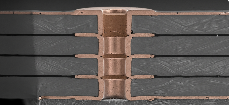
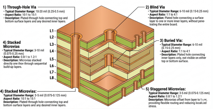
A stacked via is a design that involves two or more vias that are stacked directly on top of each other, in the same vertical axis, to form a continuous connection across different layers. With a standard HDI stackup, this implies that a microvia on Layer 1-2 is directly over a microvia on Layer 2-3, which might be over a buried via to deeper layers. The outcome is a single vertical column of interconnects.
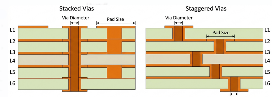
This is in stark contrast to staggered vias, in which the vias of the neighboring layers are made to be horizontally offset. In a staggered arrangement, the vias are connected to a common intermediate pad but are not in a vertical arrangement. Imagine it as a staircase vs. an elevator, staggered vias follow a stepped path through the board, and stacked vias follow a straight line.
| Feature | Stacked Vias | Staggered Vias |
|---|---|---|
| Alignment | Vertically aligned on the same axis | Offset horizontally on each layer |
| Routing density | Higher — minimal pad footprint | Lower — offset pads consume space |
| Signal path length | Shorter and more direct | Longer due to lateral offsets |
| Manufacturing complexity | Higher — requires precision alignment | Moderate — more forgiving tolerances |
| Cost | Higher due to sequential lamination and fill | Lower — standard HDI processes |
| Thermal performance | Excellent vertical heat transfer | Good but less direct |
The choice between stacked and staggered vias depends on your design constraints. Staggered vias are more forgiving to manufacture and work well for many HDI applications. But when you need maximum routing density, minimum parasitic inductance, or efficient thermal paths, stacked vias are the way to go.
Why They Are Essential for High-Density Interconnect Designs
Modern HDI designs are driven by components with extremely fine pitch BGA packages with 0.4 mm or even 0.3 mm ball pitch, for example. At these pitches, there simply is not enough room between pads to route escape traces using conventional vias. Stacked vias solve this by enabling via-in-pad designs, where the via is placed directly in the component pad, filled with conductive or non-conductive material, and capped with copper plating. This approach eliminates the need for routing traces from the pad to a nearby via, which frees up enormous amounts of routing real estate. For a 400-ball BGA with 0.5 mm pitch, switching from dog-bone fanout to via-in-pad with stacked microvias can reduce the required breakout area by 40-60%.
Key Advantages of Stacked Vias for HDI Applications
Increased Routing Density and Reduced Layer Count
The first advantage of stacked vias is that routing density dramatically increases. Since the vias are straight and are often used with via-in-pad technology, you recover board area that would otherwise be occupied by via pads, clearance,s and fanout traces.
The following is a realistic case: Take a 12-layer HDI board with four BGA components, each containing 500+ pins spaced at 0.5 mm. Using staggered vias with traditional dog-bone fanout, you might need all 12 layers just for signal routing. Reconfig to stacked microvias with via-in-pad, and you might be able to do the routing in 10 layers or redeploy those free layers to more productive power and ground plane distribution.
Reducing even two layers from a stackup has significant implications:
- Lower material cost per board
- Thinner overall board profile (critical for portable devices)
- Fewer lamination cycles in manufacturing
- Reduced drilling and plating operations
- Lighter weight for aerospace and wearable applications
Improved Signal Integrity and Shorter Signal Paths
Stacked vias have quantifiable signal integrity benefits in high-speed digital and RF designs. The straight vertical route across the board reduces the total length of the via stubs and removes the lateral trace segments across layers that a staggered via would entail. At frequencies over 1 GHz, the electrical parasitics of a via transition are an important issue. A stacked via design with appropriately designed antipads usually has a lower parasitic inductance (in the 0.2 -0.5 nH range) than staggered designs. This is equivalent to improved continuity of impedance and clean signal transitions between layers.
Key signal integrity benefits include:
- Reduced via stub effects: Stacked microvias connect only the layers needed, avoiding the long stubs of through-hole vias
- Lower parasitic inductance: The direct vertical path minimizes loop area and inductance
- Better return path continuity: Compact via structures make it easier to place return path vias nearby
- Improved thermal via performance: Stacked thermal vias create efficient heat columns from component pads to inner or outer copper planes
Design Considerations for Reliable Stacked Via Implementation
Aspect Ratio Limits and Via Stacking Rules
The aspect ratio of a via, defined as the ratio of via depth to its diameter, is one of the most critical parameters in stacked via design. In the case of mechanically drilled vias, standard processes typically have a maximum ratio of 10:1, and more advanced fabrication may have up to 12:1. Laser-drilled microvias in HDI stackups typically have a maximum ratio of approximately 0.8:1 to 1:1, and have a diameter of 75-150 um.
The following are the key design guidelines to consider in order to have a reliable implementation of stacked via:
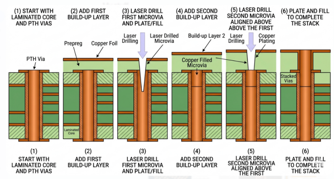
- Fill before stacking: Individual microvias in the stack are filled (with copper, conductive paste, or non-conductive epoxy) and planarized, and then the next via is drilled on top. Adding a via filler to a stack causes a hole, which cracks under thermal load.
- Keep the stack height: The majority of manufacturers suggest stacking up to 3-4 microvias in a column. On top of this, cumulative tolerances of alignment and thermal stress are hard to control.
- Select relevant capture pads: The capture and target pad size should consider layer-to-layer registration errors. The size of a normal microvia capture pad is 250-350 um in diameter with a 100-150 um via.
- Select the type of via fill: Choose conductive fill (copper - best thermal and electrical) or non-conductive fill (epoxy - less expensive, sufficient signal via fill).
- Adhere to IPC-2226 standards: IPC-2226 (Sectional Design Standard for HDI Printed Boards) gives specifications on microvia design, such as stacked via designs. It categorizes HDI buildups into Types I to VI that are based on via configurations.
- Confirm with your fabricator early: Stacked via capabilities differ greatly between vendors. Check aspect ratio limits, minimum via diameter, maximum stack count, and fill options before finalizing your design.
Integration with Layer Stackup and Thermal Management
Stacked vias are not a standalone component; they have to be a part of your overall layer stackup strategy. The stackup defines dielectric thicknesses which directly influence microvia depth and hence aspect ratios. A typical stackup of HDI is 1+N+1 or 2+N+2, referring to the number of sequential layers of buildup on each side, and N is the number of layers in the core. A 2+4+2 stackup has, as another example, two buildup layers on each side of a 4-layer core, resulting in 8 total layers with two levels of stacked microvias possible.
| Stackup Type | Total Layers | Microvia Stack Levels | Typical Application |
|---|---|---|---|
| 1+N+1 | 4-8 | 1 (single microvia) | Mobile devices, IoT modules |
| 2+N+2 | 6-12 | 2 (two stacked microvias) | Smartphones, networking equipment |
| 3+N+3 | 10-16 | 3 (three stacked microvias) | High-end processors, FPGA boards |
| Any-layer HDI | 8-20+ | All layers interconnected | Advanced SiP, military/aerospace |
Stacked vias are especially useful as thermal via arrays in thermal management, typically below power components. An array of vias stacked on a thermal pad on the topmost layer, directly to a ground plane or heatsink on the bottom layer, forms a very efficient thermal path. With a suitable density of vias and quality of fill, the thermal conductivity of a copper-filled stacked via array can be as high as 100-200 W/mK, which is much higher than the 0.3 W/mK of the surrounding FR4 material.
Manufacturing Challenges and Professional Solutions
Precision Alignment and Plating for Stacked Structures
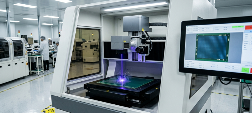
Registration of layers to layers is the largest manufacturing challenge of stacked vias. When stacking microvias, the via has to land on the filled and planarized pad of the via underneath it. When the alignment is not perfect, the via can partially miss its target pad, forming a weak joint that breaks during thermal cycling. The common registration tolerances of HDI manufacturing are 25-50 um per layer, plus or minus. These tolerances are summed up over a stack of three microvias. High-end manufacturers employ optical alignment, fiducial markings on each layer, and X-ray inspection to ensure that alignment is within acceptable limits.
The sequential plating and filling process typically follows these steps:
- Drill microvias using UV or CO2 laser
- Desmear and clean the via holes
- Electroless copper seed layer deposition
- Electrolytic copper plating to fill the vias
- Surface planarization (mechanical polishing or chemical-mechanical planarization)
- Inspection and verification of fill quality
- Laminate the next buildup layer and repeat
JLCPCB's Expertise in Stacked Via HDI Production
Advanced HDI Fabrication Capabilities for Complex Via Stacking
JLCPCB has invested heavily in HDI fabrication equipment and processes to support advanced via configurations, including stacked microvias. Their production lines handle 1+N+1, 2+N+2, and higher-order HDI stackups with the precision alignment and fill quality that stacked vias demand. Their laser drilling systems support microvia diameters down to 75 um, and their via fill processes both conductive copper fill and non-conductive epoxy fill, are qualified to meet the tight planarization tolerances required for reliable stacking. Whether you need a simple two-level stack for a compact IoT module or a complex multi-level stack for an FPGA carrier board, their capabilities cover the range.
DFM Support and High-Yield Manufacturing
The Design for Manufacturability (DFM) review process of JLCPCB on stacked via designs is one of the most valuable parts of working on stacked via designs. Once you upload your Gerber files, they verify your design via settings, aspect ratios, pad size,s and stackup compatibility with their engineering team before they start production. This initial DFM inspection identifies any problems early on - microvias too large to match the suggested aspect ratio, captured pads that are smaller than they can be reliably registered, or fill requirements that are not explicitly defined in the fabrication notes. It is better to identify these problems before production to save time, money, and frustration.
Their quality control processes include:
- Automated optical inspection (AOI) at each buildup layer
- X-ray inspection for via fill quality and alignment verification
- Cross-section analysis on coupon samples per IPC-6012 standards
- Electrical testing (flying probe or fixture-based) on finished boards
FAQ about Stacked Vias
Q: What is a stacked via in PCB design?
A stacked via is a configuration where two or more vias are placed directly on top of each other along the same vertical axis. Each via connects adjacent layers, and by stacking them, you create a continuous vertical interconnect spanning multiple layers. The vias must be filled and planarized before the next via is drilled on top.
Q: What is the difference between stacked vias and staggered vias?
Stacked vias are vertically aligned on the same axis, while staggered vias are offset horizontally from each other on adjacent layers. Stacked vias offer higher routing density and shorter signal paths but require more complex manufacturing. Staggered vias are easier and cheaper to manufacture but consume more routing space.
Q: How many microvias can be stacked?
Most manufacturers support stacking two to four microvias reliably. Beyond four levels, cumulative registration tolerances and thermal stress risks increase significantly. Check with your specific manufacturer for their maximum supported stack height.
Q: Are stacked vias more expensive than standard vias?
Yes. Stacked vias require sequential lamination cycles, laser drilling, via filling, and planarization at each level, all of which add processing steps and cost. However, the overall board cost may be comparable or even lower if the stacked vias allow you to reduce the total layer count.
Conclusion
Keep Learning
Enhancing PCB Reliability: A Deep Dive into VIA-in-PAD Design
Key Takeaways Space Saving: VIA-in-PAD (POFV) places vias directly inside SMD pads, maximizing routing channels and board miniaturization. Flawless Soldering: Epoxy filling and copper capping eliminate the risk of solder siphoning, ensuring flat, perfectly solderable pads. Maximum Performance: Direct vertical paths under components drastically lower thermal resistance and eliminate high-speed parasitic inductance. JLCPCB DFM Targets: Maintain mechanical via hole diameters between 0.25 mm and 0.35 mm, ......
How Stacked Vias Enable Higher Density and Better Performance in HDI PCBs
Key Takeaways Stacked vias are a critical technology that enables higher routing density and superior performance in HDI PCBs. By vertically aligning microvias in a single column, often combined with via-in-pad designs, they dramatically reduce breakout area, shorten signal paths, lower parasitic inductance, and improve thermal conductivity compared to traditional staggered vias. While requiring precise sequential lamination, via filling, and strict design rules, stacked vias help designers reduce lay......
Via in Pad (VIP) Technology : Driving Density and Reliability in Advanced PCB Fabrication
Via in pad is exactly what it sounds like: placing a via directly within a component’s soldering pad rather than routing it off to the side with a short trace. While this concept seems straightforward, it represents a significant evolution in PCB design philosophy that has become essential for modern high-density interconnect (HDI) boards. In traditional PCB design, vias were always placed outside the component pad area, connected by a short fanout trace. This approach works fine when you have plenty ......
Understanding Multilayer PCB Design in Modern Electronics
Introduction As electronics changes quickly, people want devices that are smaller and more powerful. This has led to the development of more advanced printed circuit board (PCB) designs. Multilayer PCBs are very important for meeting these needs because they offer higher density, when better usefulness in a smaller package. The complicated PCBs are used in a lot of high-performance devices, like smartphones, telecommunications gear, medical devices, and industrial machines. This article covers with a ......
Comparing High-Density PCB Stack-Up With Normal PCB
High-density printed circuit boards (PCBs)are not the same as simple PCBs. Do you know what the difference is? PCBs with a larger number of layers and a higher density of traces are known as HDIs. These are not as common because they are not used in small prototypes or hobby work, but for more professional application. One of the best examples of an HDI board with a complex stack-up that you can see—or might have—is the motherboard of your PC. HDI changes the story completely when it comes into the pi......
High-Density Interconnect (HDI): Revolutionizing PCB Design for Modern Electronics
In the world of advanced electronics, High-Density Interconnect (HDI) technology has become a game-changer. As devices get smaller, faster, and more complex, traditional printed circuit boards (PCBs) often face limitations in handling these demands. That’s where HDI PCBs come into play. This article covers what HDI is, why it’s critical, and how it’s shaping the future of modern electronics. 1. What is High-Density Interconnect (HDI)? A "HDI" printed circuit board (PCB) is one type whose wire count pe......