
Maximize Efficiency with PCB Panelization in High-Volume Manufacturing
12 min
- Common Panelization Methods and Layout Strategies
- Design Guidelines to Enable Seamless Panelization
- Advanced Panelization in Professional Fabrication
- How JLCPCB Elevates Panelization for Superior Results
- Frequently Asked Questions (FAQ)
Whenever a new PCB designer begins to spin the wheels, they are soon enough faced with the transition of creating a few prototypes into a volume production venture. As well as that, change brings a new idea that prototype-based engineers tend to forget: PCB panelization. In essence, panelization refers to loading a number of copies of your board design (or even a variety of designs) onto a single standardized production panel such that all of the fabrication and assembly processes treat them as a single unit. Why does this matter? Because modern fabrication and assembly equipment, from CNC drills and etching lines to solder paste printers and pick-and-place machines, is designed to handle panels, not individual small boards.
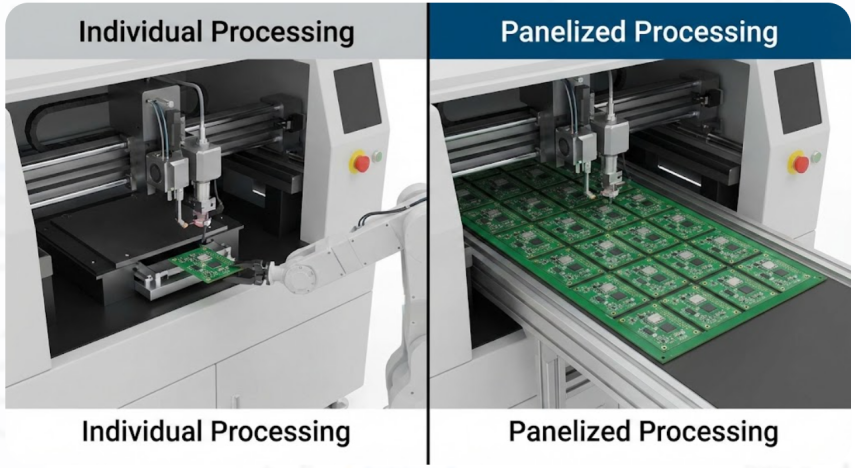
A 30mm square IoT sensor board processed individually would crawl through production at a fraction of the speed and many times the cost of the same board panelized twenty-up on a standard panel. The economics are straightforward: more boards per panel means more boards per production hour, less material waste, and lower cost per unit. For any production quantity above a few dozen, panelization is not optional; it is essential.
Core Benefits: Reduced Waste, Faster Processing, and Consistent Quality
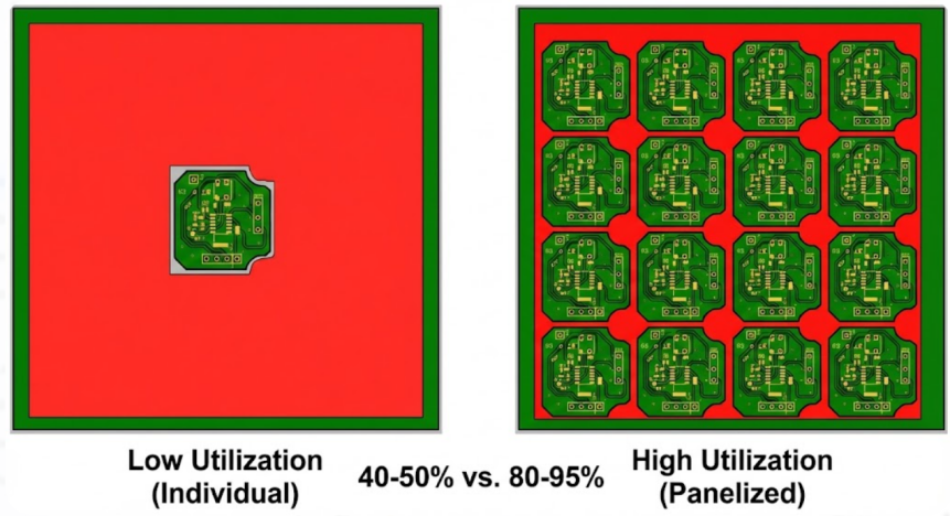
The cascade of benefits from proper PCB panel design touches every aspect of production. Material utilization jumps from perhaps 40-50% (individual processing) to 80-95% (optimized panelization), depending on board geometry and panel layout. This is not trivial — FR-4 laminate is a significant cost driver, and a 40% improvement in utilization translates directly to the bottom line.
Throughput increases in proportion to the number of boards per panel. A panel carrying 16 boards moves through each process step once, delivering 16x the output per handling operation compared to individual processing. For SMT assembly, this multiplier effect is particularly dramatic: one stencil print, one placement cycle, one reflow pass, sixteen assembled boards.
Quality uniformity is the often-overlooked third benefit. Boards sharing a panel experience identical processing: same etch chemistry, same plating current density, same reflow profile. This inherent uniformity reduces variation and makes quality control more effective and meaningful.
Pro-Tip: When quoting production costs, always compare pricing at the panel level, not the board level. A board that seems expensive individually may become very competitive when panelized efficiently.
Common Panelization Methods and Layout Strategies
V-Scoring, Tab Routing, and Breakaway Rails Explained
Three primary separation methods define how individual boards are connected within a circuit board panel and how they will eventually be separated.
V-Scoring cuts V-shaped grooves into the top and bottom surfaces of the panel along the board boundaries, leaving approximately one-third of the total board thickness as connecting material. After assembly, boards are separated by running the panel through a V-score depaneling machine or carefully flexing along the scored line. V-scoring excels for rectangular boards, provides fast separation, and adds no width to the gap between boards. Its limitations include restriction to straight-line separations and potential stress on edge-mounted components.
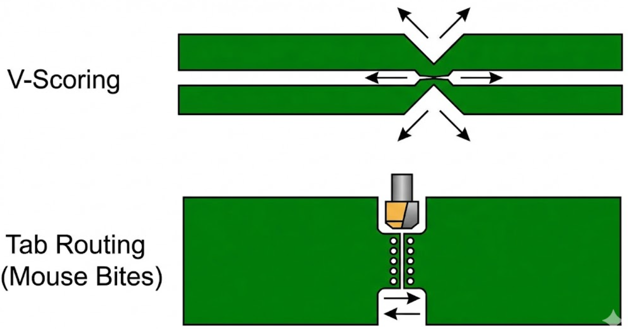
Tab Routing (breakaway tabs with mouse bites) uses a CNC router to cut the board outline, leaving only small connecting tabs with a series of overlapping drill holes (perforations). This method accommodates any board outline shape, minimizes mechanical stress during separation, and allows precise control over the connection strength. The trade-off is the routing channel between boards (typically 1.6-2.4mm), which consumes panel area.
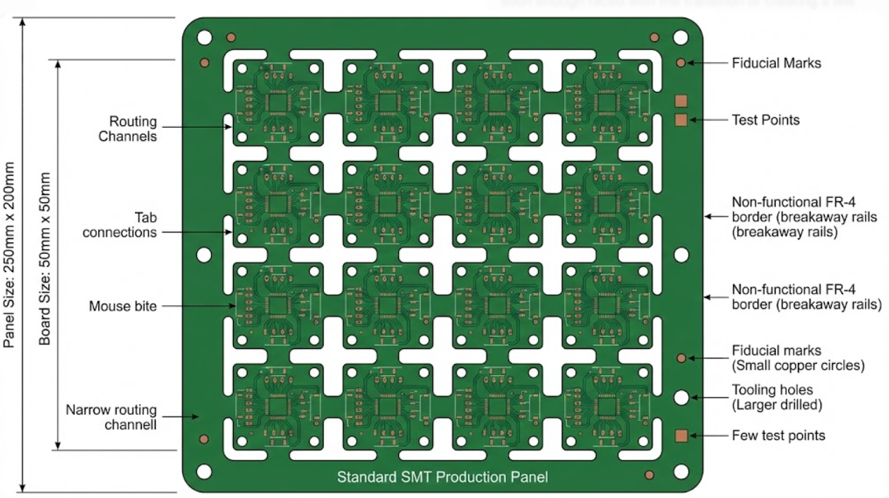
Breakaway Rails are non-functional FR-4 borders added to panel edges, providing clamping surfaces for assembly equipment and structural rigidity. Rails typically require 5mm on each side and include fiducials, tooling holes, and sometimes test points. They are standard practice for SMT panels and do not add to per-board cost since they occupy otherwise unusable edge material.
Standard Panel Sizes and Optimization for Material Utilization
Standard PCB panel size options vary by manufacturer. Commonly available working sizes include small panels around 100mm x 160mm, medium panels in the 200mm x 250mm range, and large production panels up to 457mm x 610mm or larger. The manufacturing panel (raw material size) is larger than the working area, accounting for border tooling strips.
Optimizing material utilization is a geometry puzzle: fit the maximum number of boards into the available working area while respecting minimum spacing for routing channels, maintaining structural integrity, and leaving room for rails and tooling features. Even a one-millimeter change in board dimensions can sometimes add an entire extra row of boards to a panel, delivering a meaningful per-unit cost reduction at volume.
JLCPCB’s online ordering system automatically calculates optimal panelization when you upload your design files, showing you how many boards fit per panel and providing instant cost estimates based on the optimized layout.
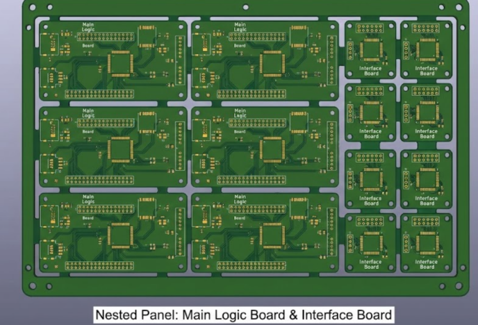
Multi-Up and Nested Designs for Complex Boards
The most common panelization is simple multi-up: identical copies of the same board in a regular grid. This is straightforward, universally supported, and the default approach for most production runs.
Nested panelization places different board designs on the same panel. This is particularly effective for product families where two or more boards are always ordered in the same quantity — for example, a main logic board and its matching interface board. Combining them on one panel synchronizes production and can improve material utilization when the boards have complementary dimensions.
The constraint for mixed panels is that all boards must share the same stackup, copper weight, surface finish, and board thickness. Different solder mask colors on the same panel are generally possible but may incur additional setup charges.
Design Guidelines to Enable Seamless Panelization
Edge Clearance, Fiducials, and Tooling Holes Requirements
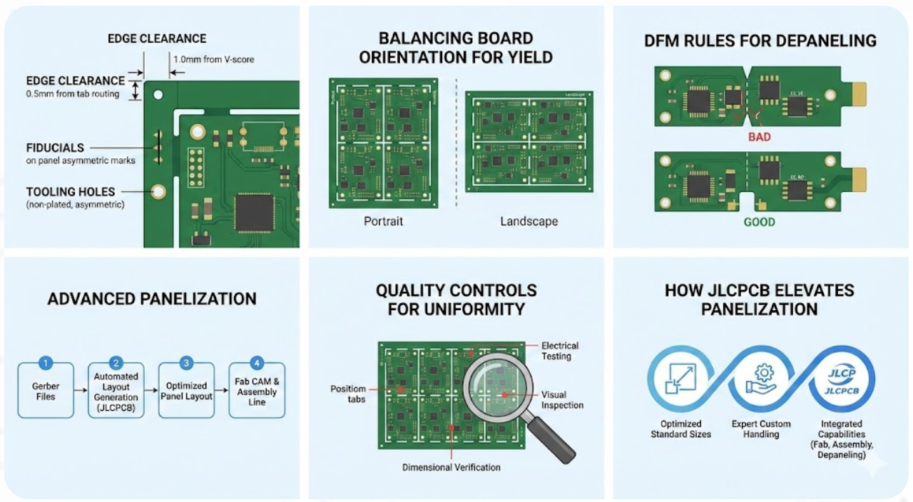
Designing for successful panelized construction means incorporating panel-level features into your design from the start. Component clearance from board edges must account for the separation method: at least 1.0mm from V-score lines (2.0mm or more for tall or stress-sensitive components) and 0.5mm from tab routing edges.
Global fiducials on the panel rails serve as primary alignment references for the SMT assembly line. Place at least three fiducials in an asymmetric pattern to allow the pick-and-place machine to determine panel position and rotation unambiguously. Local fiducials on individual boards improve placement accuracy for fine-pitch components.
Tooling holes in the panel rails (typically 2.0mm to 4.0mm diameter, non-plated) provide mechanical registration for automated handling equipment. Place them asymmetrically to prevent panel loading in the wrong orientation.
Balancing Board Orientation and Rotation for Yield
Board orientation within the panel affects both material yield and assembly quality. For maximum material utilization, try both portrait and landscape orientations (and combinations) to find the layout that fits the most boards per panel. Automated panelization tools evaluate these options instantly.
From an assembly perspective, consistent orientation simplifies reflow profile development and inspection programming. If you must use rotated orientations for yield, verify that the thermal profile remains adequate for all orientations — asymmetric copper distribution can cause different thermal characteristics depending on board rotation.
For wave soldering applications, orient boards so that the longest dimension of fine-pitch components runs perpendicular to the direction of travel through the solder wave. This minimizes solder bridging and improves yield.
DFM Rules for Depaneling and Structural Integrity
Bad panelization design becomes a headache during the depaneling step. Too close to the separation lines, you will be left with mechanical stress, which will crack solder joints or even break components. Thin boards that lack sufficient support tabs may not be supported and may sink during the printing of solder paste, which disturbs deposition. And when the V-scores are not seen, you may get an instance of board delamination along the separation line.
The following are the rules that must be adhered to: maintain all components and copper at least 1.0mm away from V -scores and 0.5 mm away from tab routes; ensure that panels remain rigid enough to print solder paste (flex no more than 0.5 mm under stencil pressure); design tabs with sufficient strength to be handled and yet weak enough to part cleanly; and provide sufficient tabs to ensure that the panel does not warp during reflow (thermal expansion can flatten unsupported areas).
Pro-Tip: Always request sample depaneling from your manufacturer before committing to a production run. A quick test with five panels can reveal separation issues that save thousands of boards from potential damage.
Advanced Panelization in Professional Fabrication
Automated Layout Generation and Process Integration
In other words, the fabricators are totally automated and panelized. When we put our Gerber files into JLCPCB, their system really examines the board outline, the copper, and the component layout to print out a sweet, optimized panel layout. It takes into account all the fines, the routing channel widths, rail dimensions, fiducial and tooling holes, the separation between the panels, and the equipment limits altogether.
The panel information they provide us with directly enters the fab CAM and assembly line programs, keeping the translation between the physical panel and all the rest (drill programs, stencils, pick-and-place coords, inspection recipes) right on course.
Handling Mixed Boards and High-Density Panel Configurations
On more complex projects, we have more than 90 percent efficient panels, mixed-design all crammed in one panel, or in row and column mash-ups with boards of varying sizes fitting together like pieces of a puzzle. All that needs to be tweaked to ensure that density is high but still printable.
Sliver-thin spacing in high-density configs is agony both in the fab and the assembly side: the tight routing channels increase the chance of bit deflection, and there is less space to place the solder paste stencils and the pick-and-place nozzles. Seasoned liars understand what is possible and can refer you to the most favorable compromise.
Quality Controls for Uniformity Across the Entire Panel
Panel-level quality control ensures that boards at every position on the panel meet specifications. This includes electrical testing of all board positions (not just edge coupons), visual inspection for position-dependent defects (edge boards may experience slightly different plating thickness), and dimensional verification of the panel registration to ensure accurate depaneling.
Statistical process control at the panel level identifies trends that per-board inspection might miss. For example, a systematic offset in drill registration that affects all boards at one panel position equally would be invisible in random board sampling but shows up clearly in panel-level analysis.
How JLCPCB Elevates Panelization for Superior Results
Optimized Standard Panel Sizes for Cost-Effective Production
JLCPCB’s production equipment is calibrated around optimized standard panel sizes that balance material utilization, equipment throughput, and quality consistency. These standard sizes have been refined through processing millions of panels and represent the sweet spot for cost-effective production across the widest range of board dimensions.
Expert Handling of Custom Panelization and High-Yield Outputs
When standard panelization does not fit your needs — unusual board shapes, mixed designs, specific orientation requirements — JLCPCB’s engineering team provides direct support for custom panel design. They bring experience from thousands of custom panelization projects to optimize your specific layout for maximum yield and reliable assembly.
Integrated Capabilities Ensuring Reliable Depaneling and Delivery
The presence of fabrication, assembly, and depaneling under a single roof, therefore, implies that JLCPCB essentially streamlines the process of panelization to the end. They ensure that the design of the panel that provides the optimal yield is still compatible with the limitations of the assembly line and the capabilities of the depaneling equipment, even prior to production. This entire process strategy holds back these expensive surprises that occur when you only optimize one step.

Frequently Asked Questions (FAQ)
Q. What is PCB panelization in simple terms?
PCB panelization is the process of arranging multiple individual circuit boards onto a single large manufacturing panel. This panel moves through all fabrication and assembly steps as one piece. It dramatically improves production efficiency and lowers per-unit cost compared to processing boards individually.
Q. How do I choose between V-scoring and tab routing?
Use V-scoring for rectangular boards with no components near the edges; it is faster and adds no inter-board spacing. Use tab routing for irregular shapes, boards with edge-mounted connectors, or when you need cleaner separation edges with less mechanical stress on nearby components.
Q. What is the best panel size for minimizing cost?
The best panel size is the one that fits the most boards with the least wasted space. This depends entirely on your board dimensions. JLCPCB’s online system automatically calculates optimal panelization and shows you the most cost-effective option when you upload your design files.
Q. Can different board designs share the same panel?
Yes, as long as they share the same layer stackup, board thickness, copper weight, and surface finish. Mixed panelization works well for board pairs that are always ordered together. Discuss mixed-panel options with your fabricator to understand any additional setup requirements.
Q. What happens if my board is too close to the panel edge?
Components too close to V-score lines or tab routing edges risk mechanical damage during depaneling. Solder joints may crack, and components may be stressed. Maintain minimum clearances of 1.0mm from V-scores and 0.5mm from tab routes, increasing to 2.0mm for tall or sensitive components.
Keep Learning
How Modular PCB Design Simplifies Complex Electronics Projects
Key Takeaway Modular PCB design simplifies complex electronics by breaking boards into independent, reusable functional blocks with clear interfaces. It boosts reusability, speeds up debugging, enhances team collaboration, and reduces errors.Shift from flat to modular design for faster development and more scalable, reliable PCBs. Ever seen a 400+ component schematic and got your head scrambled before even beginning routing? You are not alone. With the ever-increasing density of electronics combined w......
Your Ultimate Guide to PCB Rulers
In the world of PCB design and manufacturing, having the right tools is crucial for achieving accuracy and precision. One such tool that has gained popularity among professionals and hobbyists is the PCB ruler. This specialized measuring tool is designed to provide accurate measurements, reference information, and component footprints, assisting designers, engineers, technicians, and assemblers in various stages of PCB development. In this guide, we'll explore what a PCB ruler is, the features and mea......
Understanding the Materials Used in PCBs: Selection, Types, and Importance
Key Takeaways FR-4 is the go-to material for most cost-effective and reliable PCBs. Use Rogers for high-frequency and RF applications to reduce signal loss. Higher copper weight (2oz) improves current and heat handling. Choose High-Tg substrates for better thermal stability in multilayer boards. Green LPI soldermask offers the best balance of performance and inspection. Printed circuit boards (PCBs) are an essential component of modern electronics. These boards connect and support electronic component......
How to Select Tg of PCB ?
What is the Tg of PCB? In PCB manufacturing, "Tg" stands for Glass Transition Temperature. It is the temperature at which the PCB substrate material transitions from a rigid, glassy state to a soft, rubbery state. PCBs are flame-retardant (UL94 V-0) and do not burn easily; instead, they soften above Tg. The Critical Correlation Between Tg and Z-Axis CTE (Coefficient of Thermal Expansion) When the temperature exceeds the Tg point, the PCB substrate material (such as standard FR-4) undergoes a physical ......
How to Choose the Thickness of PCB
First, In the world of electronic products, the PCB is often referred to as the "heart" of the device. It interconnects all components, making board thickness one of the most important parameters. Choosing the right PCB thickness directly affects the electrical performance, mechanical stability, thermal management, and long-term reliability of the final electronic product. The process of selecting PCB thickness is influenced by various factors, such as product application scenarios, board material, an......
PCB Copper Pour Basics
What is Copper Pour in PCB Design? Copper pour refers to the technique of filling unused areas of a PCB's copper layers with solid copper planes. These planes are connected to power or ground nets, creating a continuous conductive path. Copper pour is typically used in the power and ground planes, as well as in signal layers for specific purposes. Purpose and Benefits of Copper Pour: Copper pour is primarily used to fill unused areas on PCB copper layers with solid (or hatched) copper connected to pow......