
The Benefits of Bed of Nails Testing in Professional PCB Manufacturing
13 min
- Understanding Bed of Nails Testing
- Key Benefits for High-Volume Production
- Designing Effective Bed of Nails Fixtures
- Integration in the Manufacturing Process
- JLCPCB's Advanced Bed of Nails Testing Capabilities
- Frequently Asked Questions (FAQ)
Have you ever wondered how manufacturers can test thousands of PCBs daily and not make the production line crawl? The answer, as frequently as not, is a deceitful-appearing device called a bed of nails test set-up. The platform contains hundreds of little spring-loaded pins on it, and each of those pins is aligned very precisely to touch a specific test point on your circuit board. It can check the electrical integrity of a whole PCB, shorts, opens, and component defects in a few seconds, before the board has even been off the factory floor.
Testing is no option if you are making PCBs in any significant quantity. The difference between the delivery of dependable products and warranty returns. The bed of nails test was a key element of professional PCB manufacturing decades ago, and although newer testing methods, such as flying probe, have become more common, it still holds the gold standard in high-volume production. It is almost impossible to replace when throughput is a factor, due to its speed, repeatability, and fault coverage.
Today, we will dive headfirst into the operation of the bed of nails testing, why it remains the most used quality assurance technique in high volume manufacturing, and how you can design your PCBs to make the most out of this tremendously powerful quality assurance technique. We will also consider the way JLCPCB is using this technology in their production workflow to produce boards with a high degree of reliability at scale.
Understanding Bed of Nails Testing
What Is Bed of Nails Testing and How It Works
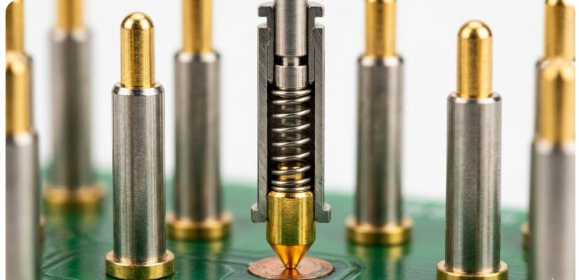
A bed of nails tester is a special electronic test fixture mainly applied in in-circuit testing (ICT) of electronic printed circuit boards. The name is quite literal. The connection is formed by a rigid plate (usually of epoxy phenolic glass cloth laminate, G-10), an array of spring-loaded pins, often referred to as pogo pins, in drilled holes. The pins are then placed to contact a specific test point, via, or pad on the PCB being tested.
The following is how it works in practice. The device under test (DUT) is the PCB that is mounted on the fixture. The board is pressed down on the pins by a mechanical press, vacuum system, or clamshell mechanism, compressing the internal springs to make a reliable electrical contact at each test point at the same time. It occurs with a single movement, with hundreds or even thousands of nodes being probed by the test system. After establishing contact, the test system feeds the system with signals and measures electrical parameters such as resistance, capacitance, inductance, voltage, and current at each node. The measured values are automatically checked and contrasted with the expected values of the board netlist and bill of materials. Any over/under tolerance in the programmed tolerances causes the board to be considered a failure, and the fault location and type are determined.
Why It Remains Essential in Modern PCB Production
It may seem to you that a testing technique that dates back to the 1960s was long overdue. However, here is the point: no other form of testing can provide the combination of speed, coverage, and per-unit cost that a bed of nails test set can provide at scale. Contemporary ICT systems based on bed of nails fixtures commonly realize defect detection rates of over 95 percent, and some systems have a defect detection rate of 98 percent or more.
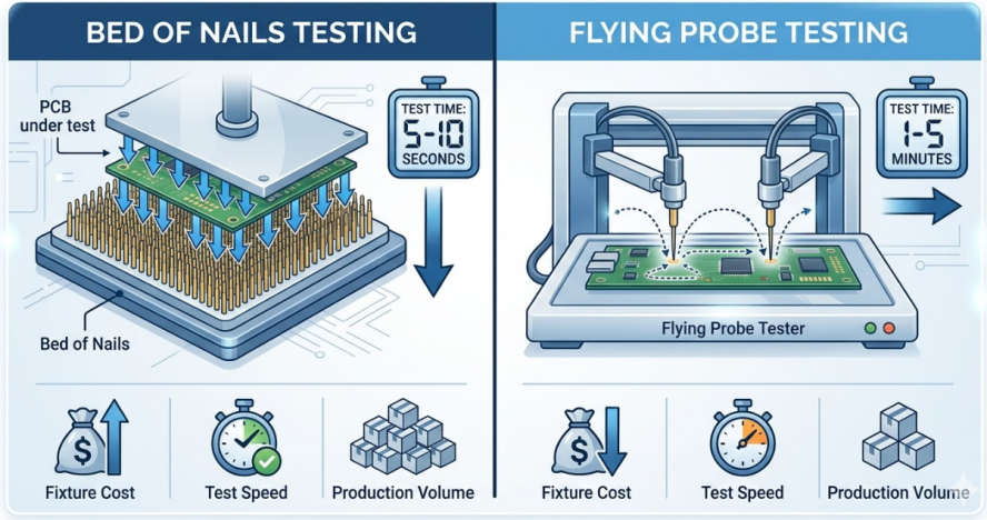
With the advent of flying probe testing, the landscape has certainly shifted, and it is a great alternative to prototypes and low-volume quantities. But flying probe testers travel one point at a time, so test times of 1 to 5 minutes per board are compared to less than 10 seconds with a bed of nails test. That difference is directly translated into throughput and cost when you are running production batches of 1,000 or larger.
| Parameter | Bed of Nails (ICT) | Flying Probe |
| Test Speed per Board | 5-10 seconds | 1-5 minutes |
| Fixture Required | Yes (custom per design) | No |
| Initial Setup Cost | $10,000-$50,000 | Minimal |
| Per-Board Test Cost (high volume) | ~$0.10 | $0.50-$2.00 |
| Defect Coverage | 90-98% | 70-80% |
| Best For | High-volume production (1,000+ units) | Prototypes and low-volume runs |
| Set up Lead Time | 2-6 weeks | Hours (programming only) |
Key Benefits for High-Volume Production
High-Speed Testing and Comprehensive Fault Detection
The most obvious benefit of bed of nails testing is the speed. Since probes are all contacted at the same time, the fixture allows all available nodes on the board to be tested in parallel. No step-by-step probing, no waiting to have a robotic arm move between points. When the board is pressed down and the contact is made, the test system is able to measure all the circuit paths simultaneously. But it is no good rushing without precision. The actual strength of the bed of nails testing is the extensive fault detection capabilities. The following kinds of defects can be identified by a well-designed ICT fixture:
- Short circuits between traces, pads, or planes
- Open circuits caused by broken traces, cold solder joints, or missing components
- Incorrect component values (wrong resistor, wrong capacitor)
- Missing components that were not placed during assembly
- Reversed polarity on diodes, electrolytic capacitors, and ICs
- Solder defects, including bridging, insufficient solder, and tombstoning
- Wrong component placement (correct part, wrong location)
Cost Efficiency and Improved Yield Rates
Be frank about the economics. A special bed of nails apparatus is not inexpensive. A fixture may range between 10,000 to $50,000, depending on the complexity of the PCB and the amount of test points. It is a huge initial investment, and that is why this process would not be reasonable when it comes to prototypes or one-off construction.
But things change drastically on volume in math. When the programmed and completed fixture is constructed, the cost of per-board test is reduced to about $0.10 or less. Take that against 0.50 to 2.00 per board of flying probe testing and the breakeven point is evident. In most designs, the bed of nails test is more cost-effective than the flying probe at approximately 500-1,000 unit level.
Designing Effective Bed of Nails Fixtures
Probe Placement and Fixture Accuracy
The success of a bed of nails test fixture relies completely on the alignment of the probes with test points on your PCB. An imprecise probe does not merely result in a false reading. It can break the board or bend the pin or even fail to hit the test point all together causing false failures to slow down your production line.
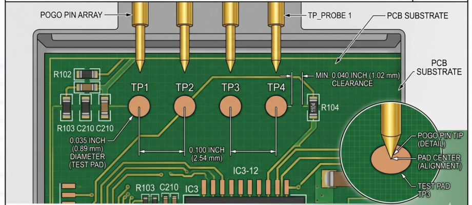
The first important choice is pogo pin. Standard test probes are available in a variety of pitch configurations, the most common and least expensive being 100-mil (2.54 mm) center-to-center. On higher-density boards, 75-mil and 50-mil probes are used, but are more expensive and have reduced operational life. There are also ultra-fine probes with 15-mil centers, which are used where the most difficult applications are possible, however this type of probe has a much higher maintenance requirement.
Here are the key design guidelines for test pad layout on your PCB:
- Test pad diameter: 0.035 inches (0.89 mm) nominal, acceptable range 0.015 to 0.040 inches
- Minimum test pad spacing: 0.050 inches (1.27 mm), with 0.100 inches (2.54 mm) preferred
- Clearance from components: At least 0.040 inches (1.02 mm) from nearby components on the same side
- Test pad density: Should not exceed 12 pads per square inch to maintain board coplanarity
- Surface finish: Solder-coated or ENIG pads provide the most reliable probe contact
Considerations for Complex and High-Density Boards
PCBs are increasingly becoming densely populated, and that poses real problems to bed of nails fixture design. A single-sided method of fixing may not be adequate when the component pitch is less than 0.5 mm, or when both sides of the board are covered with SMD components.
The other problem with a high-density board is that the accuracy of the fixtures needs to be maintained over thousands of test cycles. Pogo pins wear out. Gold-plated quality beryllium copper pins generally have a life of 100,000 to 500,000 cycles, although pins in high-stress locations or those in contact with rough surfaces will wear out sooner. It needs a proper preventive maintenance program.
| Fixture Type | Access | Best Application | Relative Cost |
| Standard Press-Down | Bottom side only | Single-sided SMT boards | Low |
| Vacuum Hold-Down | Bottom side only | Thin or flexible boards | Medium |
| Clamshell (Dual-Side) | Both sides | Double-sided SMT assemblies | High |
| Hybrid (Fixed + Flying) | Both sides + hard-to-reach | Ultra-high-density designs | Highest |
Integration in the Manufacturing Process
In-Line Testing During Fabrication and Assembly
Bed of nails fixtures are employed in electrical testing immediately after the boards are off the production line in the case of bare board fabrication. This test also checks continuity (all connections that are supposed to be there are there) and isolation (there are no unwanted connections between nets). In large-volume bare board testing, it is much faster than flying probe testing, and it prevents fabrication errors before the boards are ever put on the assembly line.
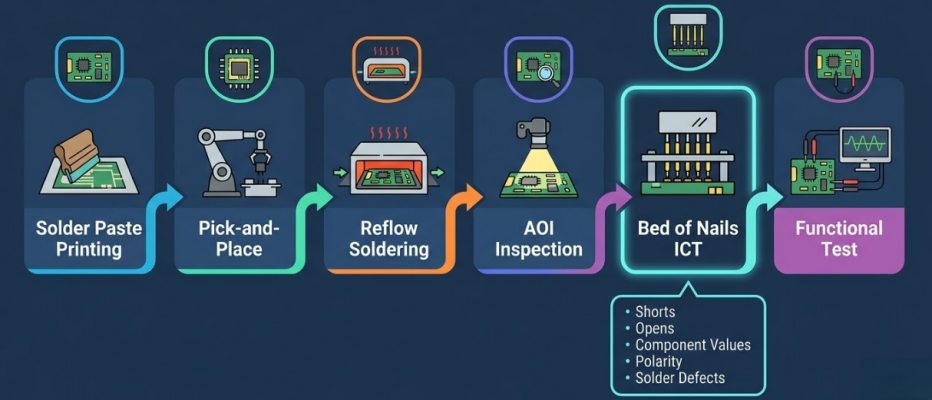
The bed of nails ICT fixture is normally placed in PCB assembly (PCBA) after reflow soldering but prior to functional testing. The process of testing in a standard SMT assembly line is as follows:
1.Solder paste printing and inspection (SPI)
2.Pick-and-place component mounting
3.Reflow soldering
4.Automated Optical Inspection (AOI)
5.Bed of nails in-circuit test (ICT)
6.Functional test (FCT)
7.Final quality control (FQC)
Ensuring Consistent Quality Before Delivery
It is consistency that distinguishes between professional manufacturing and all the rest. A bed of nails setup, previously tested and verified, provides the same test condition to each and every board going through it. The probe positions are not wandering. The spring constants determine the mechanical contact force. The pass-fail levels are programmed and fixed.
Standards such as IPC-9252 (Requirements for Electrical Testing of Unpopulated Printed Boards) and IPC-A-610 ( Acceptability of Electronic Assemblies ) determine the quality standards against which the test results are compared and thus determine this repeatability. When a manufacturer claims that all the boards have been electrically tested, it is the bed of nails fixture (or its flying probe equivalent) that is doing the work.
JLCPCB's Advanced Bed of Nails Testing Capabilities
State-of-the-Art Equipment and Custom Fixture Expertise
JLCPCB has spent a lot of money on automated Electrical testing infrastructure in its production plants. In the case of bare board testing, all PCBs leaving the fabrication line are electrically tested. In the case of standard and high-volume orders, it implies bed of nails fixtures that have probe plates that are custom-drilled to fit each board design. Flying probe testers are used to verify the same without the investment in a fixture in the case of prototypes and low-volume orders.
The difference that JLCPCB has in this respect is the speed at which they can turn around custom test fixtures. Although an average cycle of fixture fabrication in the business takes 4-6 weeks, JLCPCB has the in-house capabilities of designing and producing the fixtures, making the process much faster. Their CAM engineers extract the data on the location of the fixtures based on the Gerber files, and are guaranteed a high level of probe-to-pad alignment.
Seamless Quality Control for Reliable High-Volume Output
For engineers and product teams running high-volume production, JLCPCB's testing infrastructure means you do not need to set up your own ICT stations or invest in fixture development separately. The testing is built into the manufacturing process, and the results feed directly into their quality management system.
A few specific capabilities worth highlighting:
- Automated bare board electrical testing on every production panel, verifying continuity and isolation against your netlist
- Custom ICT fixture development for PCBA orders, with probe layouts generated from your Gerber and BOM data
- Test data logging and traceability, supporting IPC Class 2 and Class 3 quality requirements
- Integration with JLCPCB's online ordering system, where you can specify testing requirements and review quality reports
When working on a board that is going to be put into volume manufacturing, it is worth considering the testability early on. To make sure that your design is accessible to the fixtures, add special test pads to your circuit board, keep the spacing of probes to a minimum, and refer to the DFM guidelines provided by JLCPCB. When you scale to production, a bit of planning up front will save you a lot of time and money.
Frequently Asked Questions (FAQ)
Q1: What exactly is a bed of nails test fixture?
A bed of nails test fixture is a mechanical platform containing an array of spring-loaded pogo pins that align with test points on a PCB. When the board is pressed onto the fixture, every pin makes simultaneous contact with its corresponding test point, allowing the test system to measure electrical parameters across all nodes in parallel.
Q2: How is bed of nails testing different from flying probe testing?
The key difference is parallel versus sequential testing. A bed of nails fixture contacts all test points simultaneously and completes a test in 5 to 10 seconds. A flying probe tester uses movable probes that test points one at a time, taking 1 to 5 minutes per board. Bed of nails testing requires a custom fixture (costing $10,000 to $50,000) but offers very low per-unit testing costs at volume.
Q3: What types of defects can a bed of nails tester detect?
A bed of nails ICT system can detect shorts, opens, missing components, incorrect component values, reversed polarity, solder defects (bridges, cold joints, insufficient solder), and wrong component placements.
Q4: At what production volume does bed of nails testing become cost-effective?
The general industry guideline is that bed of nails testing becomes more economical than flying probe testing at volumes around 500 to 1,000 units, depending on board complexity and fixture cost. For a fixture costing $20,000 with a per-test cost of $0.10, the breakeven against flying probe testing at $1.00 per board occurs at approximately 22,000 divided by the cost difference, or roughly 22,000 boards if you factor in the fixture amortization.
Q5: How should I design my PCB to be compatible with bed of nails testing?
Design your test pads with a nominal diameter of 0.035 inches (0.89 mm), maintain at least 0.050 inches (1.27 mm) spacing between test points (0.100 inches preferred), keep test pads at least 0.040 inches from nearby components, and limit test pad density to 12 per square inch.
Q6: How long do pogo pins in a bed of nails fixture last?
Quality pogo pins made from beryllium copper with gold plating typically last between 100,000 and 500,000 test cycles, depending on the probe style, contact surface conditions, and maintenance practices.
Keep Learning
Your Ultimate Guide to PCB Rulers
In the world of PCB design and manufacturing, having the right tools is crucial for achieving accuracy and precision. One such tool that has gained popularity among professionals and hobbyists is the PCB ruler. This specialized measuring tool is designed to provide accurate measurements, reference information, and component footprints, assisting designers, engineers, technicians, and assemblers in various stages of PCB development. In this guide, we'll explore what a PCB ruler is, the features and mea......
Understanding the Materials Used in PCBs: Selection, Types, and Importance
Key Takeaways FR-4 is the go-to material for most cost-effective and reliable PCBs. Use Rogers for high-frequency and RF applications to reduce signal loss. Higher copper weight (2oz) improves current and heat handling. Choose High-Tg substrates for better thermal stability in multilayer boards. Green LPI soldermask offers the best balance of performance and inspection. Printed circuit boards (PCBs) are an essential component of modern electronics. These boards connect and support electronic component......
How to Select Tg of PCB ?
What is the Tg of PCB? In PCB manufacturing, "Tg" stands for Glass Transition Temperature. It is the temperature at which the PCB substrate material transitions from a rigid, glassy state to a soft, rubbery state. PCBs are flame-retardant (UL94 V-0) and do not burn easily; instead, they soften above Tg. The Critical Correlation Between Tg and Z-Axis CTE (Coefficient of Thermal Expansion) When the temperature exceeds the Tg point, the PCB substrate material (such as standard FR-4) undergoes a physical ......
How to Choose the Thickness of PCB
First, In the world of electronic products, the PCB is often referred to as the "heart" of the device. It interconnects all components, making board thickness one of the most important parameters. Choosing the right PCB thickness directly affects the electrical performance, mechanical stability, thermal management, and long-term reliability of the final electronic product. The process of selecting PCB thickness is influenced by various factors, such as product application scenarios, board material, an......
PCB Copper Pour Basics
What is Copper Pour in PCB Design? Copper pour refers to the technique of filling unused areas of a PCB's copper layers with solid copper planes. These planes are connected to power or ground nets, creating a continuous conductive path. Copper pour is typically used in the power and ground planes, as well as in signal layers for specific purposes. Purpose and Benefits of Copper Pour: Copper pour is primarily used to fill unused areas on PCB copper layers with solid (or hatched) copper connected to pow......
How to Prevent Solder Bridges for Superior PCB Quality and Reliability
Key Takeaways Solder bridges are a leading cause of SMT failures on fine-pitch components. Prevent them with proper solder mask dams (0.075–0.1mm), optimized stencil design, and controlled reflow profiles. Combine good DFM practices with AOI + X-ray inspection for maximum reliability. Professional manufacturing and early DFM review significantly boost first-pass yield and reduce costly rework. You have experienced the post-reflow sadness and eyed the board that failed on the first reflow, if you have ......