Understanding PCB Dielectric Constant : Choosing Materials for Optimal Signal Performance
12 min
- Common PCB Materials and Their Dielectric Constants
- How to Choose the Right Dielectric Constant for Your Design
- Manufacturing Considerations for Consistent Dielectric Performance
- JLCPCB's Expertise in Dielectric-Optimized PCB Production
- FAQ about PCB Dielectric Constant
- Conclusion
Key Takeaways
The PCB dielectric constant (Dk) is a critical factor that directly determines signal propagation speed, characteristic impedance, and transmission loss in high-frequency designs. Selecting the right material — from standard FR4 for general use to low-Dk Rogers, PTFE, and LCP for multi-gigahertz applications — enables better performance, tighter impedance control, and reduced signal degradation. Success ultimately comes from matching Dk to your frequency needs, optimizing layer stackup, and partnering with a capable manufacturer for consistent results.
Ever wonder why two PCBs of the same geometry can have very different performance at high frequencies? It typically depends on one material property that's silently controlling the speed, impedance, and loss of your signals throughout your board. That property is the PCB dielectric constant, and it is one of the most critical things that you can do to ensure you design reliable and high-performing circuits. Measuring the ability of the insulating material between copper layers to store electrical energy, relative to a vacuum, is called the dielectric constant (Dk, sometimes also referred to as the relative permittivity, Er).
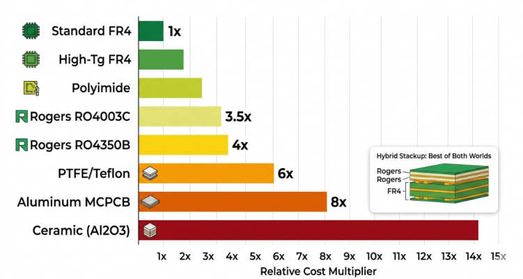
Although it would sound like a number on a datasheet, it's not abstract. The Dk of the surrounding substrate directly affects the speed of a signal down a trace, the impedance of the trace, and the amount of energy loss along the trace, each time a signal passes down the trace. Therefore, in this article, we will delve deeper into the PCB dielectric constant, discuss its significance, and compare the characteristics of various popular PCB materials, including FR4, Rogers, PTFE, and polyimide.
Definition and Basic Role in Signal Propagation
The dielectric constant is the ratio of the permittivity of the material to the permittivity of free space (Dk = 1.0 (vacuum)). It is a practical measurement which indicates the retardation of an electromagnetic wave in a material with respect to the speed of light in a vacuum. It's a simple correlation. The propagation delay of the signal through a PCB trace is directly proportional to the square root of the effective dielectric constant of the PCB trace. This formula is:
Propagation delay (tpd) = (sqrt Dk_eff)/c
In this case, c is the speed of light (3 x 10^8 m/s), and Dk_eff is the effective dielectric constant that the signal is subjected to. This equates to about 6 ps/mm of propagation delay for a microstrip trace on standard FR4. If a stripline configuration is used, then the entire trace is encircled by dielectric, and the delay is approximately 7 ps/mm. The greater the Dk is, the slower the propagation of the signal. The lower the Dk, the faster the signal moves. This has a direct impact on designs that need to match propagation delay, like DDR memory interfaces or high-speed serial links.
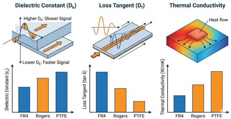
How Dielectric Constant Affects Impedance and Signal Speed
One of the main variables in all of the impedance calculations is the dielectric constant. The characteristic impedance of a microstrip trace depends on the width of the trace, the thickness of the dielectric (above the reference plane), the thickness of the copper, and the Dk of the substrate. In general, the higher the Dk, the lower the impedance for a given physical geometry. Let's take a brief peek at the effect of Dk on important signal parameters:
| Parameter | Higher Dk Effect | Lower Dk Effect |
|---|---|---|
| Signal Speed | Slower propagation | Faster propagation |
| Characteristic Impedance | Lower (for the same geometry) | Higher (for the same geometry) |
| Trace Width (for target Z0) | Narrower traces needed | Wider traces needed |
| Wavelength on Board | Shorter wavelength | Longer wavelength |
| Coupling Between Traces | Increased coupling | Reduced coupling |
Common PCB Materials and Their Dielectric Constants
Standard FR4 and Its Typical Dk Values
It's no secret why FR4 is the most popular PCB laminate used in the industry. It provides a good combination of mechanical strength, thermal stability, and cost. The dielectric constant of the typical FR4 PCB is between 4.2 and 4.7 at 1 MHz, varying with different grades and manufacturers.
But there is something that many designers miss: the Dk of FR4 is not linear with frequency. A typical FR4 laminate may have a Dk of 4.2 to 4.4 at 1 GHz. Increase the frequency to 10 GHz, and it may decrease a little to 4.0 - 4.2. This characteristic is a function of frequency and is one of the reasons why FR4 is an issue for frequencies higher than a few gigahertz, which corresponds to a high dissipation factor (Df) of 0.017 to 0.025.
Low-Dk Materials for High-Frequency Applications (Rogers, PTFE, etc.)
As your design moves to the multi-gigahertz realm, standard FR4 becomes a problem. Loss of signal increases, impedance is more difficult to control, and the variation in Dk over frequency creates timing uncertainty. Specialty low-Dk materials come into play here. The table below compares the most common high-frequency PCB materials:
| Material | Dk (at 10 GHz) | Df (at 10 GHz) | Tg (C) | Typical Application |
|---|---|---|---|---|
| Standard FR4 | 4.2 - 4.4 | 0.017 - 0.025 | 130 - 180 | General-purpose, digital |
| Rogers RO4003C | 3.38 +/- 0.05 | 0.0027 | >280 | RF, microwave, 5G |
| Rogers RO4350B | 3.48 +/- 0.05 | 0.0037 | >280 | RF, radar, automotive |
| Rogers RT/duroid 5880 | 2.20 +/- 0.02 | 0.0009 | N/A (PTFE) | Millimeter-wave, satellite |
| Isola Astra MT77 | 3.00 +/- 0.05 | 0.0017 | >200 | High-speed digital, 5G |
| Taconic TLY | 2.20 +/- 0.02 | 0.0009 | N/A (PTFE) | Aerospace, mmWave |
| Panasonic Megtron 6 | 3.40 +/- 0.04 | 0.0020 | >200 | High-speed networking |
Flex PCB Dielectric Constant Considerations
Flexible PCBs come with their own set of dielectrics. The most common flex substrate is polyimide (often known by the DuPont trade name Kapton), which has a dielectric constant typically ranging from 3.2 to 3.5 at 1 MHz.
There are a few unique factors that affect the flex PCB dielectric constant:
- Adhesive layers: For many flex constructions, an adhesive layer is placed between the polyimide film and the copper foil, either acrylic or epoxy. The combined Dk of the complete stackup is dependent upon all of the layers, and these adhesive layers also have their own Dk values (usually 3.0 – 4.0).
- Bend radius: Flex circuits will bend, and the thickness of the dielectric will slightly vary at the bend point. This changes the local effective Dk and may impact impedance in dynamic flex applications.
- Adhesiveless constructions: Adhesiveless laminates (adhesiveless construction is the term used when the copper is directly deposited or laminated onto the polyimide) offer more predictable and lower Dk performance for high-frequency flex applications.
- LCP (Liquid Crystal Polymer): LCP substrates are a premium alternative to polyimide and have Dk as low as 2.9 to 3.1 with extremely low Df for flex circuits running at frequencies above 10 GHz.
How to Choose the Right Dielectric Constant for Your Design
Matching Dk to Frequency, Layer Stackup, and Application Needs
The first question you should ask yourself is: What is the maximum signal frequency of your board? This one parameter can greatly reduce the range of materials you can select. The following is a practical guideline for materials to be used according to the operating frequency:
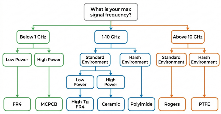
Below 500 MHz: Standard FR4 works perfectly. The variation in Dk is very small over this frequency range, and the loss of signal is small for most lengths of trace.
2 GHz to 6 GHz: Evaluate low-Dk versions of FR4 or hybrid stackups with Rogers for critical RF layers and FR4 for digital layers. The "transition zone" is where material selection becomes very important.
At frequencies above 30 GHz, PTFE-based materials (RT/duroid, Taconic TLY) or advanced ceramics are generally needed. Even a small change in Dk results in a large change in impedance at millimeter-wave frequencies.
Manufacturing Considerations for Consistent Dielectric Performance
Material Qualification and Process Control
PCB laminates are not all the same. For example, the Dk of FR4 depends on the type of resin used, the pattern of the weave, and even the direction of the glass fibers with respect to the path of the signals. This is called the glass weave effect, and may result in localized Dk changes of 0.2 or more in a standard FR4.
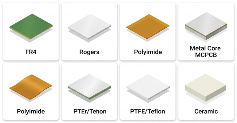
To overcome this, the PCB manufacturers in the market take a number of steps:
- Incoming material inspection: Dk and Df of each incoming lot of laminate are verified against the manufacturer's certificate of conformance (CoC).
- Controlled prepreg selection: Selecting specific prepreg styles (1080, 2116, 7628) with known percentages of resin content to get desired Dk values in the final stackup.
- Impedance test coupons: Production Panel with dedicated test coupons measured with TDR (Time Domain Reflectometry) for impedance and hence effective Dk.
Ensuring Uniformity Across Production Runs
Material qualification programs and process discipline are important for consistency between production runs. For rigid PCBs, the IPC-6012 standard, which governs the qualification and the performance specification, requires verification of the dielectric constant as part of the qualification process.
Some of the important practices to maintain the uniformity of Dk are:
- Locking the material supplier and grade: Mid-production change of the supplier or grade may result in Dks shifts, which will impact the impedance. Write down the brand and grade of laminate in your fabrication notes. Instead of just providing Dk requirements, provide the desired impedance with tolerance (e.g., 50 ohms + or - 10%).
- Asking for test coupon data: ask for TDR test reports from your manufacturer if you are using impedance-controlled boards. This data verifies design assumptions that the as-built Dk is correct.
JLCPCB's Expertise in Dielectric-Optimized PCB Production
Wide Selection of Low-Dk and High-Performance Materials
JLCPCB has a wide variety of PCB laminates ranging from FR4 to high-performance low Dk laminates. Material selections include Shengyi FR4, Rogers RO4350B for an RF front end, or a Shengyi FR4 material with Rogers RO4350B on top for an RF front end—there is no long procurement delay for any material.
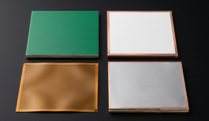
This is especially important for hybrid stackup applications where Rogers may be used for the outside RF layers and FR4 for the inside digital layers. By working with JLCPCB's engineering team, you can specify a stackup that optimizes for performance, cost, and manufacturability.
Advanced DFM Support for Precise Stackup and Impedance
A key benefit of JLCPCB is its advanced DFM (Design for Manufacturability) review process, which is one of the most practical. If you submit an impedance-controlled design, their engineering team will analyze your stackup and confirm the geometry of your traces with your target impedance before they go into fabrication.
This DFM support is comprised of:
- Recommendations of stackup based on your desired impedance and Dk requirements
- Pre-production impedance simulation to ensure your design will meet specifications.
- Material substitution guidance when your requested laminate is available in an alternative material that has the same Dk performance and is cost-effective
- TDR Test Coupon Placement for Post-Fabrication Impedance Verification
Starting at only $2, and with a turnaround time of 1-2 days for normal orders, JLCPCB makes it possible to quickly prototype your impedance-controlled designs without getting into a budget spiral.
FAQ about PCB Dielectric Constant
Q: What is the PCB dielectric constant?
The PCB dielectric constant (Dk) is a dimensionless number that describes how well the insulating substrate material between copper layers stores electrical energy compared to a vacuum. It directly affects signal propagation speed, characteristic impedance, and signal loss.
Q: Does the dielectric constant change with frequency?
Yes. All PCB materials exhibit some degree of frequency-dependent Dk variation. Standard FR4 shows more variation (Dk can shift by 0.3 to 0.5 across a wide frequency range), while premium materials like Rogers laminates are specifically engineered for Dk stability across frequency.
Q: Why is lower Dk better for high-frequency designs?
Lower Dk reduces signal propagation delay, decreases dielectric loss (which is proportional to Dk and Df), and allows wider traces for a given target impedance. Wider traces are easier to fabricate with tight tolerance, which improves impedance control accuracy. Lower Dk also reduces coupling between adjacent traces, helping to minimize crosstalk.
Q: How do I specify dielectric constant requirements to my PCB manufacturer?
The most effective approach is to specify your target impedance (e.g., 50 ohms +/- 10%) along with the laminate material and grade you have designed around. This allows the fabricator to adjust trace geometry during CAM processing to compensate for the actual Dk of the specific material lot being used.
Conclusion
The PCB dielectric constant (Dk) plays a decisive role in signal speed, impedance control, and overall high-frequency performance. Choosing the right material — from cost-effective FR4 to advanced low-Dk options like Rogers, PTFE, and LCP — is essential for meeting your design’s frequency, loss, and reliability requirements.
With proper material selection, careful stackup design, and strong manufacturing support, you can achieve excellent signal integrity while balancing cost and performance. JLCPCB offers a wide range of laminates, hybrid stackup solutions, and professional impedance control to help turn your designs into high-quality boards quickly and reliably.
Keep Learning
Choosing the Right PCB Solder Mask Material for Reliable PCBs
Key Takeaways Dual-Curing: UV defines openings; heat cures epoxy for durability. LPI vs. Coverlay: LPI for rigid boards; coverlay for flexible circuits. Color & Pitch: Green allows tighter dams (0.10 mm) than black/white (0.13 mm). Protection: Prevents solder bridges and seals copper from moisture. Cure Quality: Proper baking prevents mask peeling during plating and reflow. PCB solder mask material is a cured polymer film usually 10 to 30 µm (0.4 to 1.2 mil) thick. During reflow, it is the only barrie......
Safeguarding Circuit Boards Against Breakdown Voltage Failure
Key Takeaways Construction Matters: Breakdown voltage depends on stackup and defects, not raw material ratings. Stress Causes Failures: Heat and moisture degrade insulation over time, leading to field defects. Four Main Failure Modes: Insulation fails via internal voids, treeing, CAF growth, or surface tracking. Layout Design Fixes: Use dual prepregs, wider hole spacing, rounded trace corners, and isolation slots. Testing Split: Bare-board testing checks low-voltage net continuity, while hi-pot tests ......
Is FR4 the Best Board Material for Your Design
Key Takeaways Best All-Rounder: Ideal balance of strength, insulation, and low cost for standard PCBs. Clear Limits: Poor heat dissipation (~0.3 W/m·K) and high loss for RF (>3 GHz). Alternatives: Use Rogers for RF, Aluminum for high heat, and FPC for flexibility. Selection Essentials: Pick High-Tg (170°C+) for lead-free reflow and custom stackups for impedance. JLCPCB Advantage: 1–32 layer FR4 boards with ±10% impedance control and 24h fast dispatch. In the world of electronics and printed circuit bo......
Optimizing High-Voltage Circuit Safety with PCB Dielectric Strength
Key Takeaways Non-linear Scaling: Dielectric strength drops as thickness increases. Safety vs Signals: Dielectric strength ensures safety, while Dk controls signal speed. Material Selection: High-voltage safety depends on Tg, CTI, and moisture resistance. Spacing Rules: Clearance prevents air arcs, while creepage prevents surface tracking. Assembly Testing: Hi-pot testing requires finished assemblies, not bare boards. Dielectric strength is the number engineers quote to prove a board is safe at mains ......
How Copper Foil Shapes PCB Performance and Manufacturing Quality
Key Takeaways Weight: 1 oz copper ≈ 35 µm thickness; higher weight increases current capacity. Types: ED for standard rigid boards, RA for dynamic flex circuits. DFM & Loss: Smoother foil lowers RF loss; thicker foil requires wider trace spacing. The part of a PCB that actually carries the electrical signal is the copper foil. The strength comes from the glass weave, the resin is used to keep the layers together, and the solder mask is used to provide protection and separation of exposed copper. But w......
Why PCB Substrate Choice Matters More Than You Think
Key Takeaways Prevents Via Failures: Z-axis CTE expansion strains via barrels; right substrates prevent field failure. Specify Beyond FR-4: Name IPC-4101 sheets to guarantee proper Tg and lower thermal growth. Match Material to Need: Choose FR-4 for standard, Polyimide for flex, Aluminum for heat, and Rogers for >3 GHz. Use Real Fab Stackups: Prepreg weave alters Dk; compute impedance using real factory stackups. The PCB substrate is the one part of your board you never actually draw. You choose a thi......