Mastering PCB Trace Width to Prevent Thermal and Signal Failures
17 min
- The Hidden Risks of Getting Your PCB Trace Width Wrong
- What is PCB Trace Width and How Is It Calculated?
- Practical Rules for Standard PCB Trace Width in Modern Designs
- The Gap Between PCB Design Tools and Real Manufacturing
- How JLCPCB Delivers High-Precision Trace Width Manufacturing
- FAQ about pcb trace width
- Conclusion
Key Takeaways
- Prevent Solder Defects: Relief spokes trap heat to stop cold joints and prevent tombstoning on small parts.
- Skip Power Pads: Keep thermal pads and >3A traces solid for maximum heat escape and minimal voltage drop.
- Match Spoke Geometry: Use thin spokes (0.10–0.20 mm) for passives and wider spokes (0.20–0.30 mm) for standard SMD.
- Add Etch Margin: Size spokes 30% over fab minimums to survive over-etching during production.
When it comes to dimensions, there's one on your board that has real current, real heat, and is a real risk of failure – the trace width of a PCB. You set it in seconds in your routing, and it either holds or it doesn't. If you get it wrong, the copper overheats, the solder mask turns brown, your logic rail drops below threshold, and your board dies in a customer's hands rather than on your bench!
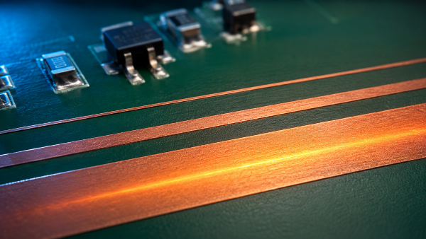
This guide explains what trace width does electrically, how the standard sizing formula works through one fully worked example, when a calculator helps and when it lies, why internal and external layers need different widths, and what your fab can actually etch.
The Hidden Risks of Getting Your PCB Trace Width Wrong
Think of a copper trace as an extension cord. A thin one runs a desk lamp all day without complaint. Plug a space heater into the same cord, and the jacket goes soft within minutes. The cord never changed, but the current did.
Your board works the same way. The trace that happily feeds an ESP32-WROOM-32 reset pin will glow if you ask it to carry a motor driver, and nothing in your EDA tool will stop you.
What is PCB Trace Width and Why It Dictates Circuit Performance
PCB Trace Width is the width of the copper on each layer of a PCB, measured in width from side to side in millimetres or mils. Copper thickness determines the cross section of the conductor, and the conductor's cross section determines the current it can carry, the voltage drop across it, and its temperature rise. Copper is not a perfect wire: it's a resistor with a very small value, and width is the way you adjust the value.
The thickness of standard 1 oz copper is approximately 35 µm (1.4 mil) and has a sheet resistance of approximately 0.49 mΩ per square. If you travel a distance of trace equal to its width, you're traversing one square, and if you travel a distance of 2 mm equal to the width, then you're crossing two squares, and so forth. When you double the width, resistance is cut in half, and heat is cut in 4.
There are three functions of width:
- Current capacity: More cross-section means more heat escapes before the trace overheats.
- Voltage drop: A narrow power trace steals supply voltage that your load never sees.
- Impedance: On high-speed nets, width sets characteristic impedance alongside dielectric height, and current is irrelevant.
Overheating, Burnouts, and Excessive Voltage Drop
A trace of 0.5 mm (20 mil) wide, 1 oz copper, 100 mm (3.9 in) from a connector to a load, with a current of 3 A. That is the 200 square path, or approximately 98 mΩ. It will lose 295 mV and lose 0.88 W of power in a copper strip as thin as a grain of rice. With the 3.3 V rail, you simply lost nine percent of the supply. Widen it to 2 mm (79 mil), and it becomes 24.6 mΩ, a 74 mV drop, and 0.22 W. As copper gets hot, it fights back! As the temperature increases, its resistance increases by approximately 0.39% per °C, so the trace generates more heat and gets hotter and hotter.
Let's take an example of A 3D printer control board. A 24 V heated bed pulling 12 A ran on 1.5 mm (59 mil) of 2 oz copper across an 80 mm (3.1 in) route, which is 13 mΩ and about 1.9 W concentrated under solder mask. After a few dozen print hours, the mask had browned, and the copper was lifting at the terminal block. Rerouting it as a 6 mm (236 mil) pour cut the loss to 0.47 W.
What is PCB Trace Width and How Is It Calculated?
The industry's answer is one empirical equation in use since the 1950s. It was not derived from first principles but curve-fitted to measurements of real boards, which is why it needs judgment applied on top.
Breaking Down the IPC-2221 PCB Trace Width Formula
The PCB trace width formula (IPC-2221) relates the current to the trace's cross-sectional area and the allowable temperature rise.
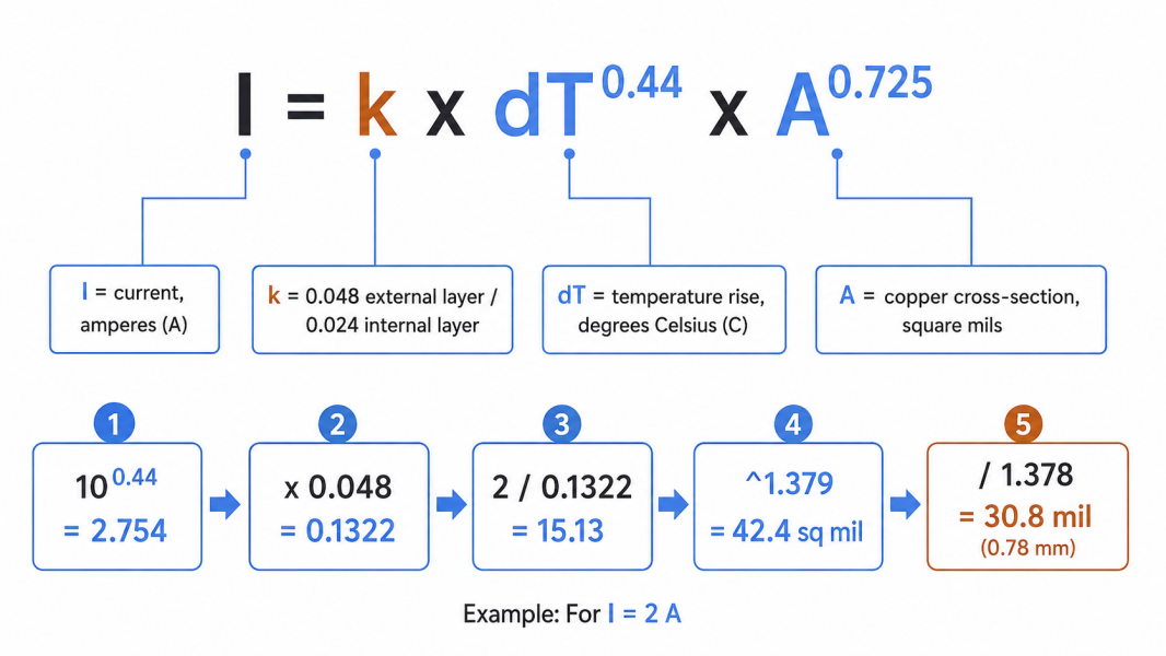
I = k × ΔT^0.44 × A^0.725
Each of the symbols is followed by its units:
- I is the current in the trace, in amperes (A).
- ΔT = the maximum temperature increase (above the board temperature) allowed, in degrees Celsius (°C). It is a change in temperature, not an absolute temperature.
- A is the cross-sectional area of the copper (mils2 or mil²).
- k is a constant value (0.048 for external traces on an outer layer and 0.024 for internal traces between dielectric layers).
You want the width from the current, so rearrange it:
A = ( I / (k × ΔT^0.44) )^(1/0.725)
Next, take the area divided by the copper's thickness. You need 2 A on an external layer, you accept a 10 °C rise, and the board is standard 1 oz copper, 1.378 mil thick.
- Raise the temperature to the 0.44 power. 10^0.44 = 2.754.
- Multiply by k for an external layer. 0.048 × 2.754 = 0.1322.
- Divide your current by that result. 2 / 0.1322 = 15.13.
- Raise that to the power 1 / 0.725, which is 1.379. 15.13^1.379 = 42.4 mil², the cross-section you need.
- Divide the area by the copper thickness. 42.4 / 1.378 = 30.8 mil.
Your answer is 30.8 mil, or 0.78 mm, about as wide as the short side of a 0603 resistor body.
| Current (A) | Width at 10 °C Rise | Width at 20 °C Rise | What This Width Means in Practice |
|---|---|---|---|
| 0.5 | 0.115 mm (4.5 mil) | 0.076 mm (3.0 mil) | Below most fab minimums, so the design rule decides, not the formula |
| 1 | 0.30 mm (11.8 mil) | 0.20 mm (7.8 mil) | A comfortable default for a general-purpose 5V or 3.3 V rail |
| 2 | 0.78 mm (30.8 mil) | 0.51 mm (20.2 mil) | Needs a real board area, so plan the route before you place parts |
| 3 | 1.37 mm (53.8 mil) | 0.90 mm (35.3 mil) | The point where 2 oz copper often beats a wider track |
| 5 | 2.77 mm (108.9 mil) | 1.82 mm (71.5 mil) | Nearly 3 mm of copper, so a polygon pour is usually better |
| 10 | 7.19 mm (283 mil) | 4.72 mm (186 mil) | No sane 1 oz route. Move to heavy copper, a plane, or a busbar. |
Manual Calculations vs. Using an Online PCB Trace Width Calculator
Use an online PCB trace width calculator for the number. Do the arithmetic by hand once so you can tell when the calculator is quietly wrong.
A calculator knows three inputs: current, temperature rise, and copper weight. It does not know your board sits in a sealed enclosure at 55 °C ambient, so your "10 °C rise" lands at 65 °C of copper. It does not know that a linear regulator is dumping 2 W two millimeters away. It does not know your 2 mm power trace necks to 0.4 mm, where it squeezes between two vias. That last one catches experienced designers constantly. A trace carries what its narrowest section allows, and that section is almost never the one you measured.
To fix this: after routing, sweep the whole power path at high zoom and find the tightest point. Size the entire net from there.
The current-carrying capacity was superseded in 2009 by IPC-2152. It is based on measured thermal data, not on mid-century curve fits, and it can be used for boards of varying thickness, having a variety of dielectric thermal conductivity, next to a variety of copper planes, and in air or vacuum.
External vs. Internal Traces: Why Location Changes the Math
The constant k halves for internal layers, from 0.048 to 0.024. Because the area sits under an exponent of 0.725, halving k does not double the required area. It multiplies it by about 2.6. Take the 2 A example again at a 10 °C rise. The external answer was 0.78 mm (30.8 mil). On an internal layer, the same formula demands 2.03 mm (80 mil), a serious amount of inner-layer real estate for a modest current.
The part that no designer has ever heard. This 50 % derating was only assumed and not measured. Engineers thought: If there is no air to convect into it, a buried trace must run hotter. When measured correctly by IPC-2152, it was found that the internal traces of the same width and current generally run cooler, as the surrounding dielectric conducts heat away better than still air convects it. An internal trace over a solid ground plane runs cooler still, because the plane spreads heat sideways, which is a quiet argument for a well-planned copper pour over isolated routing.
Practical Rules for Standard PCB Trace Width in Modern Designs
Most boards do not need a calculator for most nets. They need defaults you apply without thinking, plus the discipline to stop and calculate on the handful that matter.
- Signal and logic nets: 0.15 to 0.25 mm (6 to 10 mil): Anything drawing milliamps is thermally irrelevant, so pick a width your fab holds cheaply and stay there. This is the standard PCB trace width for most routes on a typical board.
- Power nets: about 1 mm (39 mil) of width per amp on 1 oz outer copper: Deliberately generous, roughly double what the formula demands at a 10 °C rise, and that margin absorbs etch tolerance, pad necks, and a warm enclosure.
- Never route below your fab's minimum, which, for most manufacturers, ranges from 0.09 mm (3.5 mil) to 0.15 mm (6 mil), depending on copper weight and layer count.
- Controlled impedance nets are exempt: On a 50 Ω single-ended or 90 Ω differential net, width comes from the stackup, not from current. Widening a matched trace to "be safe" breaks the thing you were protecting.
- Above 5 A, change strategy instead of widening: Move to 2 oz copper, use a polygon pour, route the net on two layers stitched with vias, or accept a busbar.
- Design for a 10 °C rise by default, and reserve 20 °C for cases where you genuinely know the ambient and the airflow.
Real hardware follows this pattern: Open a 65 W GaN USB-C charger, and the signal side is all hairline traces while the output path is a broad copper region feeding the connector. A 3 A step-down module built around an LM2596 or a TPS54331 needs perhaps 1.4 mm (55 mil) on its input and output rails and 0.2 mm (8 mil) everywhere else.
The Gap Between PCB Design Tools and Real Manufacturing
Your EDA tool draws a perfect rectangle with sharp corners. Your fab delivers a trapezoid with rounded edges. The difference between those two shapes is where a surprising number of thermal failures are born.
Copper Etching and How Thickness Alters Final Trace Width
In subtractive etching, a chemical spray is used to remove the copper, and chemistry has no respect for your outline. The etchant is drawn down, but also "under-etches" under the resist, leaving only a trapezoid section, where the base is wider at the laminate than at the top surface.
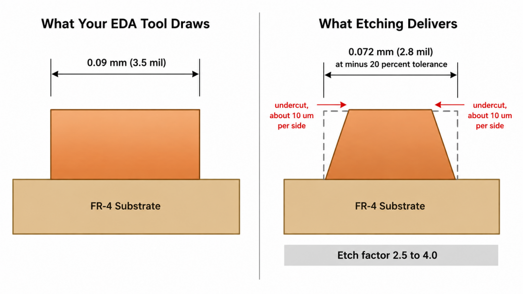
This is measured by the etch factor. The etch depth divided by the undercut on one side—the typical production values range between 2.5 and 4.0, with the exact etch depth/undercut ratio depending on the etchant chemistry.
The etch factor control becomes more important as features become smaller because the artwork is widened during the fab's pre-compensation for imaging. Design around the published tolerance: at the extremes of the published tolerance of plus or minus 20 percent, a 0.09 mm (3.5 mil) trace can arrive at 0.072 mm (2.8 mil)—25 percent more resistance and 25 percent more heat than you calculated.
What Happens When Fine Traces Push Factory Tolerances?
Push the process floor below, and the failures stop being theoretical. Hairline traces develop, opening where undercut punches through a thin section. Squeezed spacing produces shorts where a copper sliver survives etching. Controlled impedance nets drift outside their window. Boards below roughly 0.09 mm (3.5 mil) also move into a tighter process class with lower yield, which shows up as a price step and a longer lead time.
To fix this, load your fab's actual design rule file into your EDA tool rather than trusting the default 6-mil template. Most tool defaults were chosen years ago and no longer match anyone's current capabilities.
How JLCPCB Delivers High-Precision Trace Width Manufacturing
Everything above assumes your manufacturer holds its published numbers batch after batch. That consistency is what turns a calculation into a working board.
Advanced Etching Control for Ultra-Tight Trace Tolerances
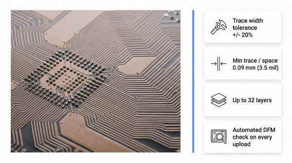
JLCPCB publishes a trace width tolerance of ±20 % and holds its minimum trace and space limits using automated etchant management and statistical process control, so the concentration and spray pressure that set your etch factor do not drift across a run.
| Copper Weight | Board Type | Minimum Trace / Space | What This Means for Your Design |
|---|---|---|---|
| 1 oz | 1 to 2 layers | 0.10 / 0.10 mm (4 / 4 mil) | Enough resolution for most fine-pitch escapes on a simple board |
| 1 oz | 4-layer and above | 0.09 / 0.09 mm (3.5 / 3.5 mil) | The tightest routing available, best saved for BGA fanout |
| 2 oz | 2 layer | 0.16 / 0.16 mm (6.5 / 6.5 mil) | Thicker copper needs more etch room, so plan wider channels |
| 2 oz | 4-layer and above | 0.15 / 0.15 mm (6 / 6 mil) | A good balance of current capacity and routing density |
| 2.5 to 4.5 oz | 2-layer only | 0.20 to 0.30 mm (8 to 12 mil) | Heavy copper for high current, at the cost of fine features |
Read the pattern rather than the rows: every step up in copper weight costs routing resolution, because thicker copper takes longer to etch and undercuts further while it does. A design needing both 2 oz copper and 0.09 mm (3.5 mil) traces needs a stackup change, not a tighter tolerance. No etch process gives you both.
Automated DFM Checks to Catch Trace Width Errors Early
Every uploaded design runs through automated DFM analysis before production, flagging trace and spacing violations, copper slivers, and copper-to-edge problems while they are still free to fix. An engineering query gets raised before the panel is imaged rather than after the boards ship. That review is a safety net, not a substitute for your own pass. Before you upload, check five things:
- Set your DRC to the fab's real minimums, not your tool's factory defaults.
- Trace the full path of every net above 1 A, from source pad to load pad, and find its narrowest point.
- Check thermal relief spokes on high-current through-hole pads. Four thin spokes can be a tighter bottleneck than the trace feeding them.
- Confirm your copper weight selection matches what your width calculation assumed.
High-Layer Stackups Built for High-Current Performance
Beyond about 5 A, the right answer stops being a wider trace and becomes a better stackup. With support for up to 32 layers, thicknesses from 0.4 mm to 4.5 mm, and inner copper at 0.5 oz, 1 oz, or 2 oz, you can give a power rail its own plane pair instead of squeezing it through a channel. A 2 oz inner plane behaves like an absurdly wide trace. Current spreads over the full plane area, resistance collapses, and heat has the whole board to escape into. That is why a laptop motherboard has almost no wide traces despite delivering tens of amps.
Vias are the piece people misjudge. A 0.3 mm (12 mil) finished via with 20 to 25 µm of barrel plating carries roughly 0.019 to 0.024 mm² of copper, about the same cross-section as a 0.54 to 0.68 mm (21 to 27 mil) wide trace in 1 oz copper. A single via is not a bottleneck, and four in a square array comfortably outrun the 2 mm trace feeding them.
FAQ about pcb trace width
Q: What is a standard PCB trace width?
For general signal and logic routing, 0.15 to 0.25 mm (6 to 10 mil) is the common default, because it carries far more than any signal needs, and every fab holds it cheaply. Power traces are sized individually from current, starting near 0.3 mm (12 mil) for 1 A on 1 oz outer copper.
Q: How wide should a PCB trace be for 1 A?
On an external layer in 1 oz copper with a 10 °C rise, the formula gives about 0.30 mm (11.8 mil), and most designers round up to 0.5 mm (20 mil) to absorb etch tolerance and pad necking. On an internal layer, the same current asks for roughly 0.78 mm (31 mil).
Q: Should I use IPC-2221 or IPC-2152 for trace width?
IPC-2152 superseded IPC-2221 for current carrying capacity and is based on measured thermal data rather than 1950s curve fits. Use the IPC-2221 formula for a fast, conservative first estimate, then switch to IPC-2152 when board area is tight.
Q: Can I use a narrower trace if I choose thicker copper?
Yes, since current capacity depends on cross-sectional area, and 2 oz copper is twice as thick as 1 oz. But thicker copper etches with more undercut, so the fab's minimum trace width rises at the same time.
Q: Why do internal traces need to be wider than external traces?
The IPC-2221 formula halves its constant for internal layers, from 0.048 to 0.024, requiring roughly 2.6 times the cross-sectional area for the same current. That derating came from an assumption that buried traces run hotter, though IPC-2152 measurements later showed internal traces often run cooler.
Conclusion
The useful shift in thinking about PCB trace width is to stop treating it as a routing style and start treating it as a component value. Every trace is a resistor with a power rating, and you set both numbers when you choose the width. The formula gives you a starting point, the tolerance tells you how much margin to add, and your narrowest section decides what the net actually does.
Size the critical nets deliberately, default the rest, and check the whole path rather than the widest part of it. As boards shrink while power demands climb, tight etch control and automated DFM are what turn a calculated width into copper that behaves the way your maths promised.

Popular Articles
• Understanding the Basics of Electronic Devices and Circuits
• Understanding Digital Circuit Timing: Setup Time, Hold Time, Contamination Delay & Clock Skew
• PCBs Explained: A Simple Guide to Printed Circuit Boards
• Guide to the Top 10 Commonly Used Electronic Components
• Digital 101: Fundamental Building Blocks of Digital Logic Design
Keep Learning
Polyimide Flex PCB: A Complete Guide for Engineers
A polyimide flex PCB can be folded about 285,000 times when the base film is 25 µm (1 mil) thick. Make that film 75 µm (3 mil), and the same MIT fold test gives up near 6,000 cycles. Bending is a strain problem, not a material problem. Copper sits above the center of the stack, so a bend forces it to stretch around the longer outer path. Figure 1: A polyimide flex circuit folded tight, with a stiffener holding the connector A thicker stack places the copper farther out, resulting in more stretch at th......
Flex PCB Bend Radius: Calculation, Minimum Radius & Design Guidelines
Flex PCB bend radius is the one dimension on an FPC that no design rule check will catch. Bend the circuit tighter than its material allows; the outer copper stretches from its elongation limit, and then it cracks. Figure 1: A flex circuit formed around a mandrel, with bend radius and stack thickness A flex circuit bends around a neutral axis near the middle of its stack. Copper below that line is squeezed, and copper above it is pulled. So the further a layer sits from the line, the harder it is to w......
Flexible Circuit Connector: Types, Features & Selection Guide
A flexible circuit connector clamps onto the bare copper at the end of a flex circuit, so nothing is soldered at that joint. The tail slides into the housing, and an actuator presses a row of spring contacts onto the pads. Every connector is built around one tail thickness. TE's 0.5 mm pitch 2328702 family expects 0.30 mm (12 mil) of flex, because the contact beams are deflected by exactly that dimension. Figure 1: Cross-section of a 0.5 mm pitch FPC connector with the tail inserted Feed it a bare sin......
FPC vs FFC: Understanding the Key Differences Between Flexible Circuit Technologies
The FPC vs FFC decision is really a question about how the copper was made. An FFC consists of flat copper strips laminated between two PET films. Every conductor runs straight from end to end at one fixed pitch, because nothing in that process can make a trace turn or branch. An FPC starts as copper-clad polyimide and is etched exactly like a rigid board. Traces can turn, taper, split onto a second layer, and land under a soldered component. The finished circuit can be as thin as 0.1 mm (4 mil). Figu......
A Comprehensive Guide to Capacitor ESR: What It Is, Good Values, and How to Measure It
Key Takeaways Definition: Capacitor ESR (equivalent series resistance) is the single resistance that represents the losses inside a real capacitor, from its electrodes, terminations, electrolyte, and dielectric. Why It Matters: Ripple current flowing through the ESR produces a ripple-voltage step on the supply rail and I²R heating in the capacitor, which limits the capacitor's ripple-current rating and service life. Conditions Matter: ESR varies with frequency, temperature, capacitance, case size, and......
Understanding IPC-6012 Standards for High-Reliability Rigid PCB Fabrication
Key Takeaways IPC-6012 vs. IPC-A-600: IPC-6012 is the binding specification, while IPC-A-600 is only for visual reference. Class 2 vs. Class 3: Class 3 requires thicker copper (25μm vs. 20μm) and zero plating voids. Coupon Verification: Quality is tested by microsectioning panel coupons after thermal stress. Upfront Callout: Specify the class on drawings upfront; boards cannot be upgraded later. IPC-6012 is the line on your fabrication drawing that decides what your supplier is allowed to ship. Most d......