
Why Sequential Lamination Delivers Superior HDI PCBs
13 min
- The Role of Sequential Lamination in Advanced PCB Technology
- The Sequential Lamination Process Step by Step
- Key Benefits for High-Performance HDI Designs
- Manufacturing Challenges and Professional Solutions
- JLCPCB's Expertise in Sequential Lamination
- Frequently Asked Questions (FAQ)
Did you ever ask yourself how smartphone manufacturers can crust a thousand connections into a credit card-sized board? The process is referred to as sequential lamination, which is a multi-cycle process that is used to fabricate PCBs on a layer-by-layer basis, releasing microvia structures and routing densities that cannot be accessed by a single-press process. Without it, the slick, high-performance electronics that we all use on a daily basis would not appear the way that they do now. With data rates exceeding 25Gbps/channel, component pitches reducing to less than 0.4mm, the traditional through-hole only multilayer boards become space-starved very quickly. BGAs with fine pitch require blind vias, buried vias, stacked microvias to fan out, maintain the clean signal, and maintain competitive sizes of the boards.

This is all made possible by sequential lamination and is the key to success when you are planning your next HDI project. When you understand how it works, today, we will have an overview of the entire sequential lamination process, that is, the fabrication of cores and laser drilling, the picking of materials, and the settings in the press. We will explore the advantages of routing density, signal integrity, and thermal management, examine the manufacturing issues, and learn how these complicated designs are transformed into functional production boards with the help of the advanced capabilities of JLCPCB. Let’s get into it.
The Role of Sequential Lamination in Advanced PCB Technology
What Sequential Lamination Is and How It Differs from Standard Lamination
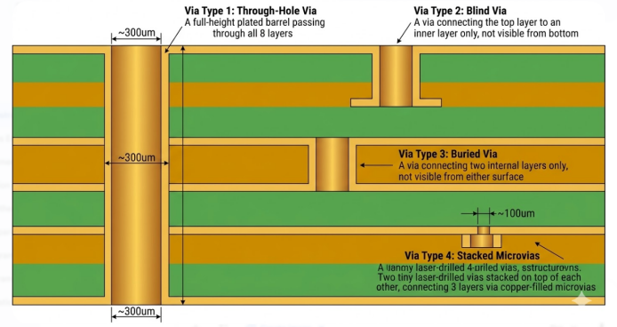
In normal multilayer PCB production, all the copper layers, the prepreg sheets, and the core laminates are simply layered and pressed once. It is just that, but you are left with through-hole vias that completely pass through the board. You cannot simply drill between two adjacent layers without drilling through their entire thickness. Sequential lamination addresses that by laminating the board repeatedly, typically two or six or more times. Once you've drilled and plated each press, so as to make blind vias (outer to outer), buried vias (inner to inner), and the little microvias (laser-drilled, around 75 to 150 microns in diameter) that are just to connect neighboring layers.
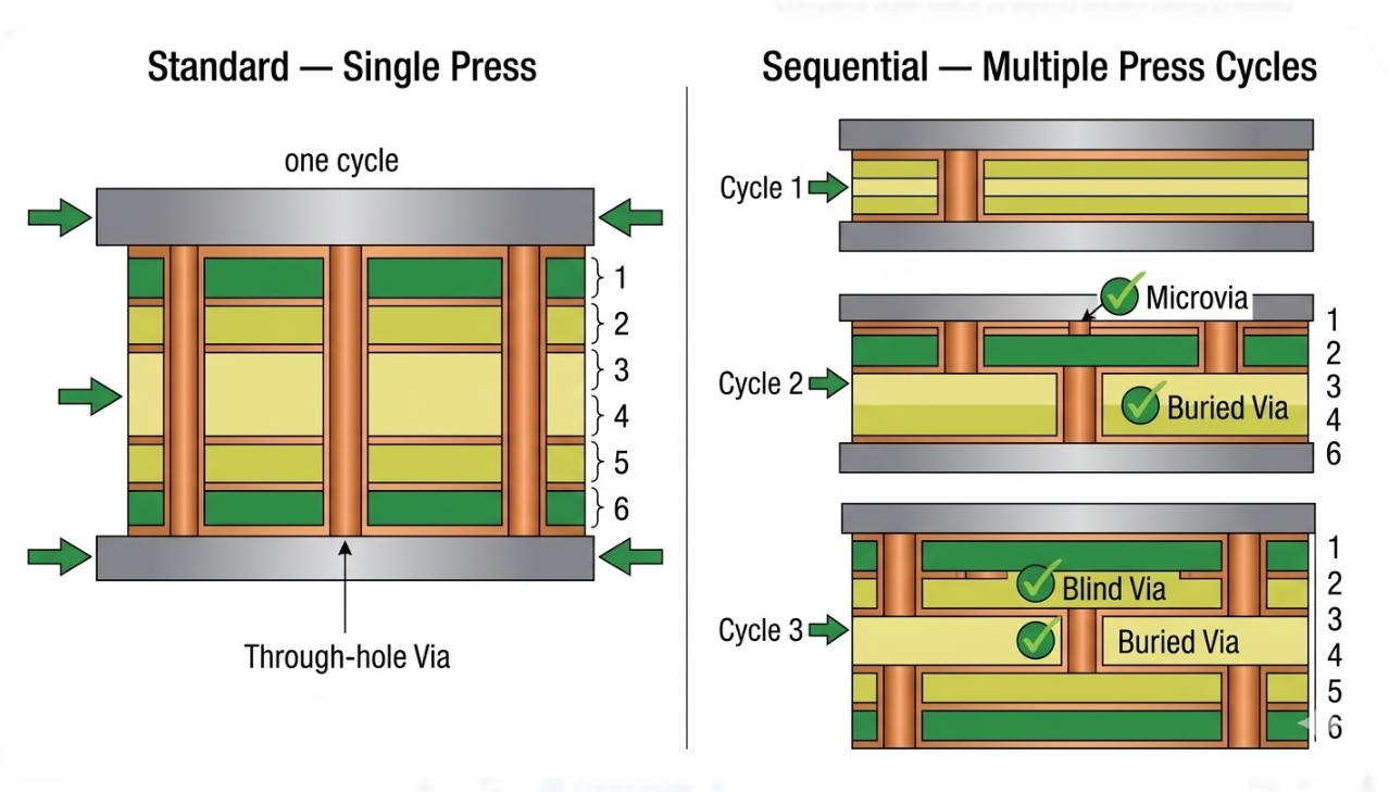
HDI build-up configurations are discussed in the industry using X+N+X notation. The 2+N+2 stack implies two build-up layers on the one hand, and two layers on the other hand. The design standard (IPC-2226) of HDI describes six types of HDI. Types I and II may occasionally obtain modified common processes, whilst types III through VI require sequential lamination due to their stacked and staggered microvia designs. The press cycles have a temperature of approximately 180 to 200 degrees, 250 to 400 PSI, a vacuum of less than 50mbar, and offer an approximate two to four hours for the fabrication time.
Why It Is Essential for High-Density Interconnect (HDI) Boards
The HDI boards are based on 0.75:1 to 1:1 aspect ratio microvias, which can only be attained if you drill and plate after each lamination step. Consider a contemporary application processor BGA, ball pitch 0.4mm. Attempting to trace those signals with conventional through-hole vias geometrically is not geometrically feasible. Sequential lamination with via-in-pad microvias has each BGA pad directly on a filled microvia, and the signals fall cleanly into the inner layers, allowing trace widths as small as 50 to 75microns. The most sophisticated variant is Every Layer Interconnect (ELIC), in which you laminate pair by pair until all the layers are laminated. Smartphones consume about 50 to 60 percent of the world's HDI PCB production, with main boards manufactured in 2+N+2 or 3+N+3 design.
The Sequential Lamination Process Step by Step
Layer Build-Up, Drilling, and Plating Cycles
The sequential lamination process follows a precise, repeating sequence. Here is how a typical HDI fabrication flow works from start to finish.
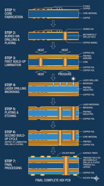
- Core fabrication: The double-sided core is imaged, etched, stripped, and AOI inspected.
- Core drilling and plating: In the case of the buried vias connecting inner layers, we drill these mechanically and then we electroplate them and then add any build-up layers.
- First build-up lamination: Prepreg and copper foil are pressed onto each side of the core under vacuum (below 50 mbar), heat (180 to 185 degrees Celsius), and pressure (250 to 400 PSI).
- Laser drilling of microvias: UV lasers (355 nm) drill microvias below 100 microns; CO2 lasers handle 100 to 150 micron microvias.
- Desmear and plating: We wipe the walls with permanganate or plasma to remove residues of resin, seed with electroless copper, and electrolytically plate to a minimum of 20-25um thickness.
- Imaging and etching: This process involves laying the circuit pattern onto the build-up layer using laser direct imaging (LDI) and then etching the pattern
- Repeat for additional build-up layers: The steps 3-6 are repeated with each added build up layer; a 3+N+3 board passes through this sequence three times on each side.
- Final processing: The last step is to drill through-holes, provide a surface finish, solder mask, silkscreen, and perform 100 percent electrical tests to complete the board.
Material Selection and Pressing Parameters for Precision
Material selection is critical because the laminate must survive multiple thermal cycles. Designers must choose FR-4 grades with a Tg of 170 to 180 degrees Celsius and a Td above 340 degrees Celsius. The Z-axis CTE should be below 3.5 percent to minimize stress on microvias during repeated pressing and reflow. For high-speed applications, low-Dk/Df materials like Panasonic Megtron 6 (Dk ~3.4, Df ~0.002) dramatically reduce signal loss compared to standard FR-4 (Dk 4.2 to 4.5, Df 0.017 to 0.025).
| Parameter | Standard FR-4 | High-Tg FR-4 | Megtron 6 |
| Dk (at 1 GHz) | 4.2 - 4.5 | 4.2 - 4.5 | ~3.4 |
| Df (at 1 GHz) | 0.017 - 0.025 | 0.015 - 0.020 | ~0.002 |
| Tg (deg C) | 130 - 140 | 170 - 180 | 185+ |
| Td (deg C) | 310 - 340 | 340 - 350 | 410+ |
Key Benefits for High-Performance HDI Designs
Higher Routing Density and Smaller Form Factors
Pad sizes of microvias 250-350 microns consume much less space compared to through-hole vias of 500-700 microns. A via-in-pad design essentially eliminates the fan-out traces on BGA pads, which is highly essential in the 0.4 to 0.5 mm pitch packages that the current processors and FPGAs are packaged in. A ton of fine-pitch packages would simply not be routable on an otherwise practical board size without via-in-pad.
The savings due to the layer count are actual. Through-hole. You can normally reduce a 12-layer design to 8 layers when you go to HDI microvias. On the average main board of a smartphone, individuals typically go with 8 to 12 layers in a 2+N+2 or 3+N+3 stackup, which is 50/50 of that micron line-space on the buildup layers, which is twice if you would see on a normal board.
Key density advantages of sequential lamination include:
- Microvia pads (250-350 microns) versus through-hole pads (500-700 microns), freeing 2-3x more routing channels between BGA pads.
- Via-in-pad eliminates fan-out routing, critical for 0.4-0.5 mm pitch BGAs.
- Layer count reduction of 30-50 percent compared to equivalent through-hole designs.
- Board area reduction of 30-60 percent, a decisive advantage in space-constrained applications.
- Fine trace capability: 50/50 micron line/space on build-up layers versus 100/100 micron on standard layers.
Improved Signal Integrity and Thermal Management
Sequential lamination is providing real, measurable signal integrity improvements in earnest. The through-hole vias through the unused layers on a standard board will eventually create stubs that resonate at high frequencies. A small stub of 1mm can begin to resonate at approximately 37.5 GHz, a signal ruffer at much lower frequencies. Blind microvias, however, simply touch the layers they require, a nd in that sense, the stubs are eliminated. Microvia parasitics are dramatically lower: 0.02 to 0.05 pF capacitance and 0.05 to 0.1 nH inductance, versus 0.3 to 0.7 pF and 0.3 to 1.0 nH for through-hole vias. This yields impedance tolerances of 5 to 10 percent lower than standard multilayers.
| Parameter | Through-Hole Via | Microvia (HDI) |
| Parasitic Capacitance | 0.3 - 0.7 pF | 0.02 - 0.05 pF |
| Parasitic Inductance | 0.3 - 1.0 nH | 0.05 - 0.1 nH |
| Impedance Tolerance | +/- 10-15% | +/- 5-10% |
| Stub Resonance Risk | Significantly above 5 GHz | Eliminated |
Sequential lamination also benefits thermal management. With more continuous ground and power planes, ground bounce and EMI are reduced. Dense arrays of thermal microvias can be placed directly under hot components, reducing thermal resistance by 30 to 50 percent compared to sparse through-hole thermal via patterns.
Manufacturing Challenges and Professional Solutions
Alignment Accuracy and Registration Control
To start with, each press cycle is a nightmare since it may be misaligned. We are looking at four to six cycles, and that is enough to add up even minute registration errors, and the specs are strict, with HDI tolerances down to ±25 to 50 microns standard. IPC-6012E Class 3 specifies ±50 microns, leaving little margin across multiple cycles.
Manufacturers address this with X-ray alignment systems (plus or minus 10 to 15 microns accuracy) and LDI systems (±5 to 10 microns). Laminates shrink 0.02 to 0.05 percent per axis per cycle, requiring artwork pre-scaling based on measured shrinkage data for each material and stackup configuration.
Avoiding Delamination and Ensuring Uniform Thickness
The scourge of PCB hobbyists and professionals is delamination. Those press cycles impose thermal stress on the bond lines, and we are talking about moisture absorption, incomplete cure, surface contamination, and the heat as a result of all those presses. That is the reason why we store the materials at less than 50% RH and pre-bake them at a temperature of 105 to 120 degrees Celsius for several hours. Moisture must stay below 0.15 percent. Copper bonding treatments target peel strength above 1.0 N/mm, well above the IPC-6012E Class 3 minimum of 0.7 N/mm. Thermal reliability is validated through six solder float cycles at 288 degrees Celsius for 10 seconds each. The Td must exceed 340 degrees Celsius, and the dielectric thickness tolerance is held to plus or minus 10 to 15 percent.
JLCPCB's Expertise in Sequential Lamination
Advanced Multi-Stage Pressing and Laser Drilling Capabilities
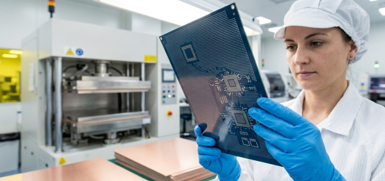
I have studied HDI boards during my electronics course, and the manner in which JLCPCB performs the heavy lifting is rather interesting. They apply vacuum lamination presses, which literally step the temperature and the pressure, and so the cure prints out uniformly, and the dielectric remains uniform. Also, they have UV and CO2 laser drilling equipment capable of punching microvias as small as 100 microns, which is enormous when it comes to putting more stuff on a board.
The facility can work to build up configurations to 3+N+3, that is, they are able to stack a bunch of layers, be they straight up or staggered and offset. The IPC-2226 spec is much discussed nowadays with respect to stackup, and it is a delight to observe an actual shop do all the variations; stacked, staggered microvias, even with copper filling where necessary.
Rigorous Quality Control for Reliable HDI Production
Following every imaging and etching process, they pass through an AOI that captures defects at 10 to 20 micron resolution before they are covered by the subsequent layer. After that, they invert it to check X-rays to make sure everything is aligned and that the microvia is of the required quality. To be even more certain, they draw test coupons to be micro-sectioned so that they can check copper thickness, dielectric uniformity, and bond integrity- in other words, all that you have read in the lab report.
All completed boards are 100 percent electrically tested, and TDR impedance testing is used to ensure controlled-impedance traces remain within a plus or minus 5 to 10 percent. The shop has been certified as ISO 9001 and listed as a UL manufacturer and passes the IPC Class 2 and Class 3 production standards - so you can be sure that the process has been tested by all the major players.
Scalable Solutions from Prototypes to High-Volume Runs
When you are creating a prototype, you can create as few as five copies. However, when the design is complete, they are prepared to increase to full-volume production. Their online instant quoting tool will provide you with a rough price on any HDI stackup, and their DFM review is the way to work out the manufacturability hassles - think of microvia aspect ratios or registration tolerances that you would otherwise bump into after a semester learning PCB design. They also provide an assortment of surface finishes, such as HASL, ENIG, OSP, immersion silver, and immersion tin. You can select the one that suits your bill the best.
When your design is taking the envelope too far, and you need more than standard PCBs can do, then sequential lamination is the route to take at JLCPCB. Sequential lamination is simply the method that allows the modern HDI PCBs to exist- you make the board layer in steps, drilling and plating between each press cycle. That is what opens microvias, blind and buried vias, via-in-pad, and the small trace geometries that the project you are working on requires. It is a little more difficult and certainly more expensive than flat lamination, but the advantages, fewer layers, smaller boards, and high-quality electrical performance, make it an indispensable part of high-tech designs.

Frequently Asked Questions (FAQ)
Q1: What is sequential lamination in PCB manufacturing?
Sequential lamination is a multi-cycle fabrication technique where the PCB is built up layer by layer, with drilling and plating performed between each press cycle.
Q2: How many lamination cycles does a typical HDI PCB require?
The number of cycles depends on the build-up configuration. A 1+N+1 design needs one extra lamination cycle per side (two total extra cycles). A 2+N+2 needs two per side, and a 3+N+3 needs three per side.
Q3: What is the difference between stacked and staggered microvias?
Stacked microvias sit directly on top of each other across multiple build-up layers, requiring copper filling of lower vias to provide a solid landing pad for the next via above. Staggered microvias are offset on successive layers, connecting through intermediate copper pads rather than stacking directly.
Q4: Why is sequential lamination more expensive than standard PCB fabrication?
The cost increase comes from multiple factors: additional press cycles (each adding 2-4 hours), laser drilling equipment and time, extra imaging and plating steps, tighter registration requirements, and more intensive inspection at each stage. Each sequential cycle adds roughly 15 to 30 percent to the fabrication cost.
Q5: What materials are best suited for sequential lamination of HDI PCBs?
Mid to high-Tg FR-4 with a glass transition temperature of 150 to 180 degrees Celsius and a decomposition temperature above 340 degrees Celsius is the standard choice. For high-speed designs, low-loss materials like Panasonic Megtron 6 (Dk 3.4, Df 0.002) or Isola IS415 are preferred.
Keep Learning
Your Ultimate Guide to PCB Rulers
In the world of PCB design and manufacturing, having the right tools is crucial for achieving accuracy and precision. One such tool that has gained popularity among professionals and hobbyists is the PCB ruler. This specialized measuring tool is designed to provide accurate measurements, reference information, and component footprints, assisting designers, engineers, technicians, and assemblers in various stages of PCB development. In this guide, we'll explore what a PCB ruler is, the features and mea......
Understanding the Materials Used in PCBs: Selection, Types, and Importance
Key Takeaways FR-4 is the go-to material for most cost-effective and reliable PCBs. Use Rogers for high-frequency and RF applications to reduce signal loss. Higher copper weight (2oz) improves current and heat handling. Choose High-Tg substrates for better thermal stability in multilayer boards. Green LPI soldermask offers the best balance of performance and inspection. Printed circuit boards (PCBs) are an essential component of modern electronics. These boards connect and support electronic component......
How to Select Tg of PCB ?
What is the Tg of PCB? In PCB manufacturing, "Tg" stands for Glass Transition Temperature. It is the temperature at which the PCB substrate material transitions from a rigid, glassy state to a soft, rubbery state. PCBs are flame-retardant (UL94 V-0) and do not burn easily; instead, they soften above Tg. The Critical Correlation Between Tg and Z-Axis CTE (Coefficient of Thermal Expansion) When the temperature exceeds the Tg point, the PCB substrate material (such as standard FR-4) undergoes a physical ......
How to Choose the Thickness of PCB
First, In the world of electronic products, the PCB is often referred to as the "heart" of the device. It interconnects all components, making board thickness one of the most important parameters. Choosing the right PCB thickness directly affects the electrical performance, mechanical stability, thermal management, and long-term reliability of the final electronic product. The process of selecting PCB thickness is influenced by various factors, such as product application scenarios, board material, an......
PCB Copper Pour Basics
What is Copper Pour in PCB Design? Copper pour refers to the technique of filling unused areas of a PCB's copper layers with solid copper planes. These planes are connected to power or ground nets, creating a continuous conductive path. Copper pour is typically used in the power and ground planes, as well as in signal layers for specific purposes. Purpose and Benefits of Copper Pour: Copper pour is primarily used to fill unused areas on PCB copper layers with solid (or hatched) copper connected to pow......
How to Prevent Solder Bridges for Superior PCB Quality and Reliability
Key Takeaways Solder bridges are a leading cause of SMT failures on fine-pitch components. Prevent them with proper solder mask dams (0.075–0.1mm), optimized stencil design, and controlled reflow profiles. Combine good DFM practices with AOI + X-ray inspection for maximum reliability. Professional manufacturing and early DFM review significantly boost first-pass yield and reduce costly rework. You have experienced the post-reflow sadness and eyed the board that failed on the first reflow, if you have ......