Logic Gate Symbols: The Complete Chart, Truth Tables [2026]
12 min
- Logic Gate Symbols Chart (Quick Reference)
- Understanding Logic Gate Symbols in Circuit Schematics
- Basic Logic Gate Symbols and Truth Tables
- ANSI/IEEE vs IEC Logic Gate Symbols: Key Differences
- How to Read the Inversion Bubble on Any Gate Symbol
- Universal Gates: Building Any Function From NAND or NOR
- Logic Gate Symbols to 74xx and 4000-Series ICs: Pinout Reference
- Conclusion
- FAQs about Logic Gate Symbols
Note
⬇ Free Download: Logic Gate Symbols PDF Reference Chart
Save time when working with digital schematics. This downloadable Logic Gate Symbols PDF includes all basic logic gates, standard symbols, truth tables, Boolean expressions, and common 74xx/4000-series IC references — a practical reference for students, engineers, and PCB designers.
When we define digital logic on a schematic, we use logic gate symbols to represent Boolean operations and show how signals are processed in a circuit. A single symbol can represent an entire logical function with only a few lines. However, one missed inversion bubble can change the output behavior, leading to design errors, debugging time, or costly board rework.
Logic gate symbols are the foundation of digital circuit design, appearing everywhere from basic logic ICs to complex embedded systems.
In this guide, you will learn:
- Every ANSI/IEEE and IEC symbol for all seven gates, side by side
- Truth tables and Boolean expressions for each gate
- How to read the inversion bubble on any gate
- Which 74xx and 4000-series IC implements each gate
- How a gate symbol becomes a PCB footprint
Logic Gate Symbols Chart (Quick Reference)
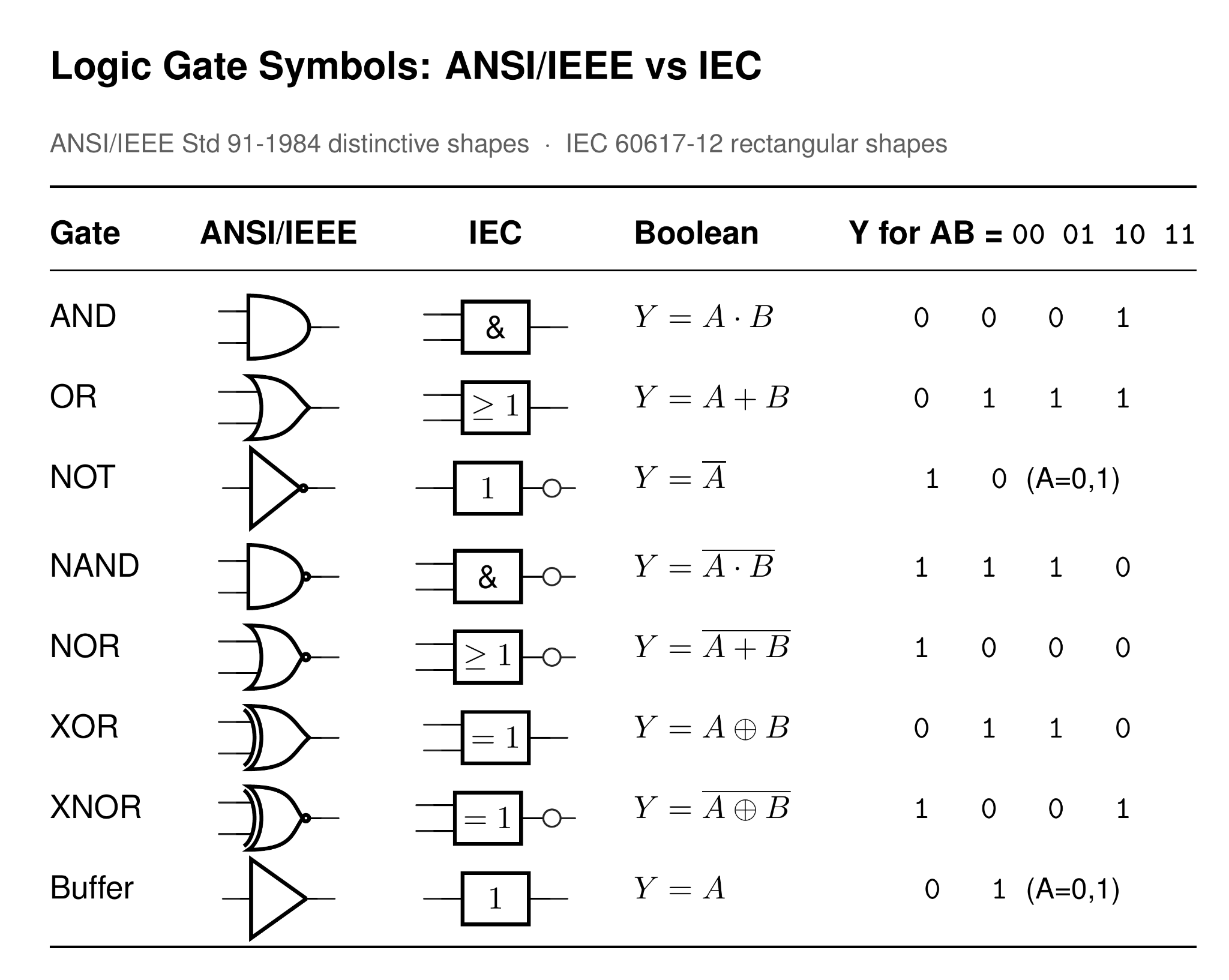
Figure: Logic gate symbols in ANSI/IEC form.
⬇ Free Download: Logic Gate Symbols PDF Reference Chart
This chart lists every basic logic gate symbol in both drawing standards, with its Boolean expression and output rule. Use it as a lookup, then jump to any gate below for its full truth table.
| Gate | ANSI/IEEE Distinctive Shape | IEC Qualifying Symbol | Boolean Expression | Output Is HIGH When |
|---|---|---|---|---|
| AND | Flat back, curved nose | & | Y = A · B | All inputs are HIGH |
| OR | Curved back, pointed nose | ≥1 | Y = A + B | Any input is HIGH |
| NOT | Triangle, output bubble | 1 | Y = A' | The input is LOW |
| NAND | AND shape, output bubble | & with negation | Y = (A · B)' | Any input is LOW |
| NOR | OR shape, output bubble | ≥1 with negation | Y = (A + B)' | All inputs are LOW |
| XOR | OR shape, doubled back | =1 | Y = A ⊕ B | Exactly one input is HIGH |
| XNOR | XOR shape, output bubble | =1 with negation | Y = (A ⊕ B)' | The inputs match |
| Buffer | Plain triangle, no bubble | 1 | Y = A | The input is HIGH |
Understanding Logic Gate Symbols in Circuit Schematics
A logic gate symbol is a standardized graphic representation of a logical function in an electronic schematic. In the common schematic convention, input signals enter from the left and the output leaves from the right. The symbol shape or internal identifier shows which Boolean operation the gate performs.
Every logic gate symbol carries three key pieces of information:
- The function identifier: The ANSI/IEEE outline shape, or IEC function symbols such as &, ≥1, or =1 inside a rectangular block.
- The negation indicator: A small circle (bubble) on an input or output pin indicates signal inversion or an active-low function.
- The pin arrangement: Inputs are typically shown on the left and outputs on the right, with pin numbers assigned after the symbol is linked to a physical component.
The two most common logic symbol systems are ANSI/IEEE-style symbols and IEC rectangular symbols. ANSI/IEEE symbols use distinctive gate shapes, while IEC 60617 defines rectangular blocks with standardized function identifiers for international use.
Basic Logic Gate Symbols and Truth Tables
The seven basic logic gates are AND, OR, NOT, NAND, NOR, XOR and XNOR. Each has its own symbol, truth table and Boolean expression. A buffer is added below because it shares the NOT gate outline.
Note
In every truth table, 1 is a logic HIGH and 0 is a logic LOW. A prime mark, as 'A', means NOT A.
#1 AND Gate Symbol
An AND gate drives its output HIGH only when every input is HIGH. Its ANSI symbol is a flat-backed D shape; the IEC form is a rectangle marked `&`.
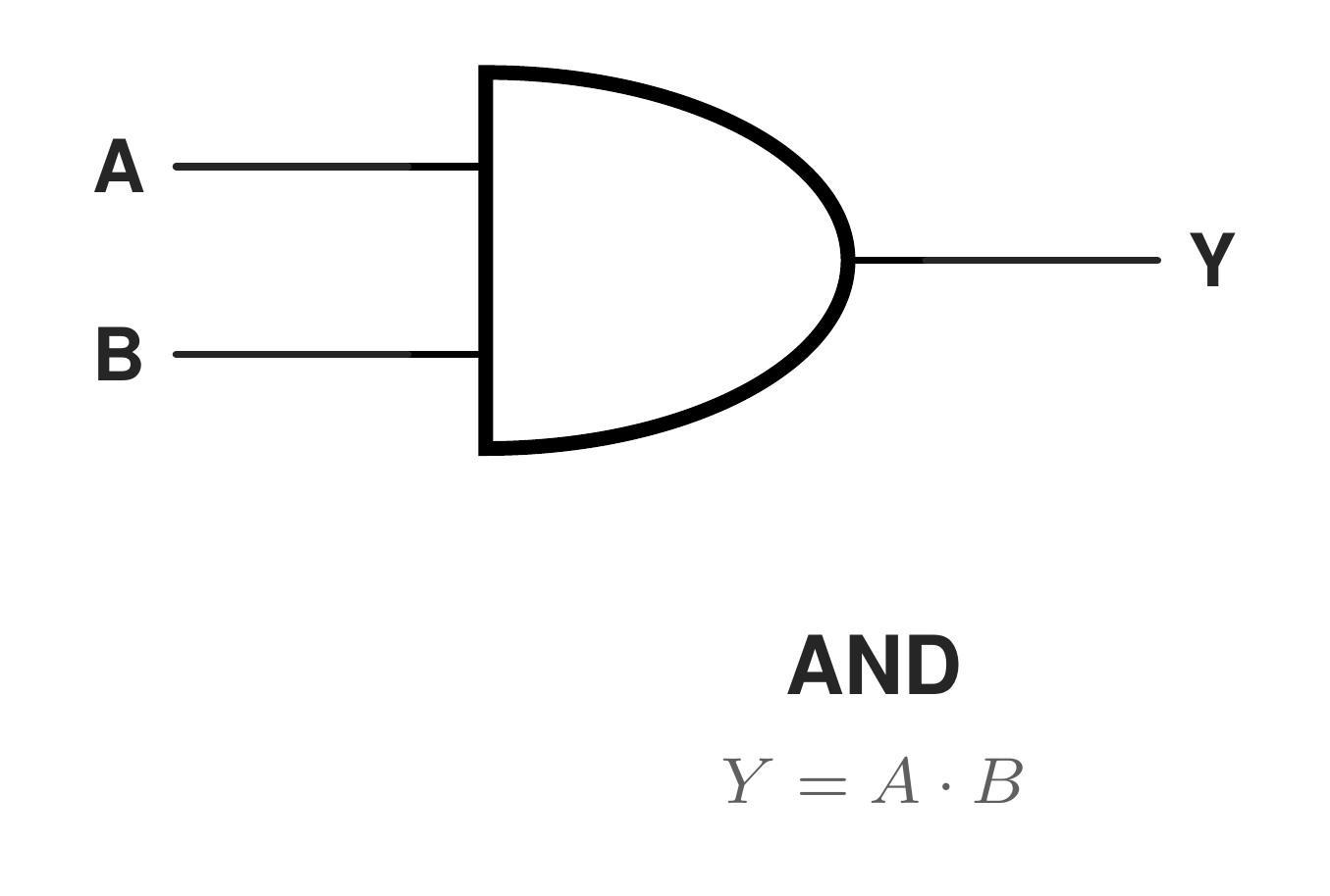
Figure: AND gate symbol with inputs A and B
| A | B | Y |
|---|---|---|
| 0 | 0 | 0 |
| 0 | 1 | 0 |
| 1 | 0 | 0 |
| 1 | 1 | 1 |
Table: AND gate truth table.
Boolean expression: Y = A · B
In practice: An AND gate gates a clock or data line, passing it only while an enable input stays HIGH.
#2 OR Gate Symbol
An OR gate drives its output HIGH when at least one input is HIGH. Its ANSI symbol has a curved back and a pointed nose; the IEC rectangle is marked `≥1`.
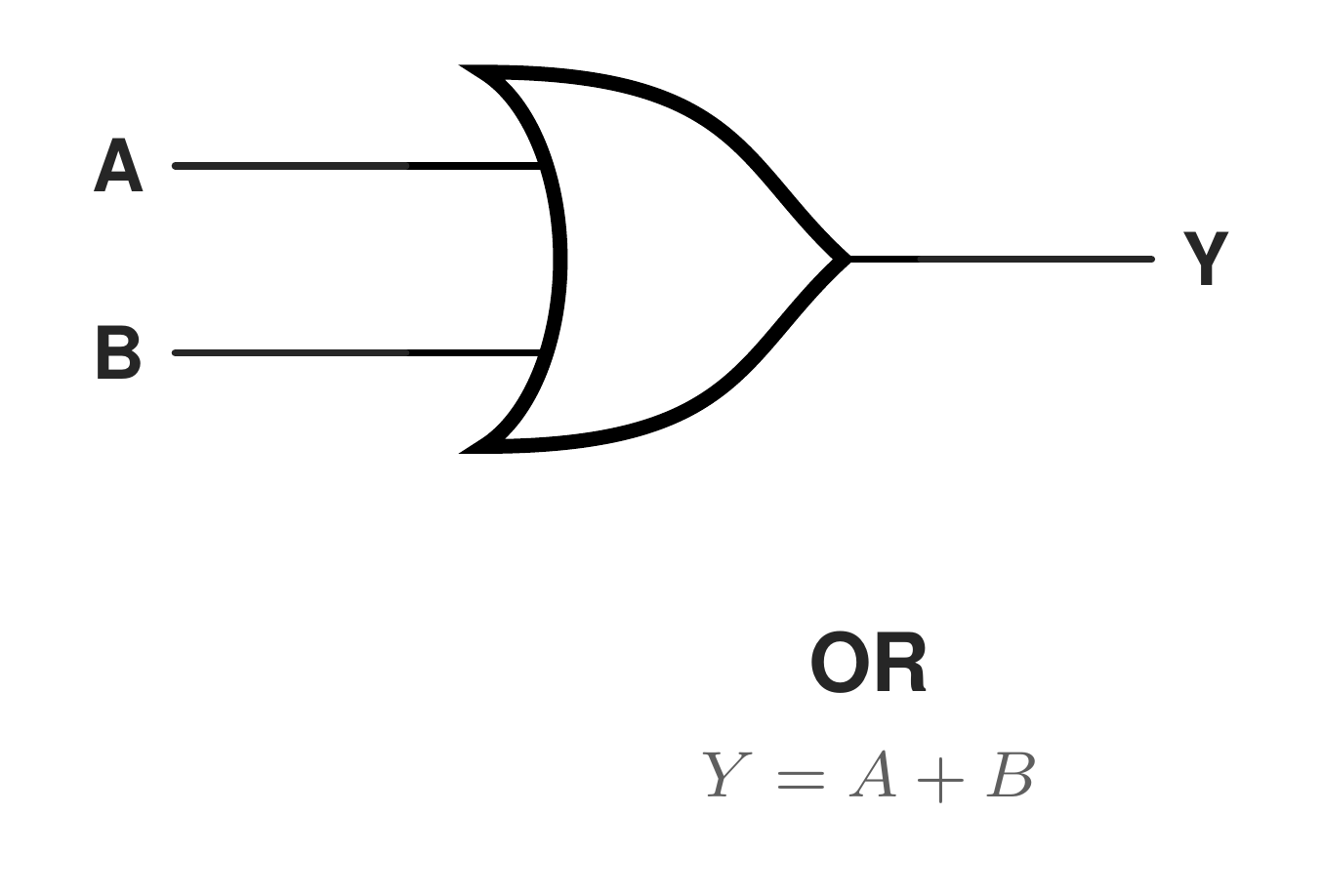
Figure: OR gate symbol with inputs A and B
| A | B | Y |
|---|---|---|
| 0 | 0 | 0 |
| 0 | 1 | 1 |
| 1 | 0 | 1 |
| 1 | 1 | 1 |
Table: OR gate truth table.
Boolean expression: Y = A + B
In practice: An OR gate merges several fault lines into one interrupt line.
#3 NOT Gate Symbol (Inverter)
A NOT gate has one input and inverts it. Its ANSI symbol is a triangle with a bubble on the output, and the bubble, not the triangle, does the inverting.
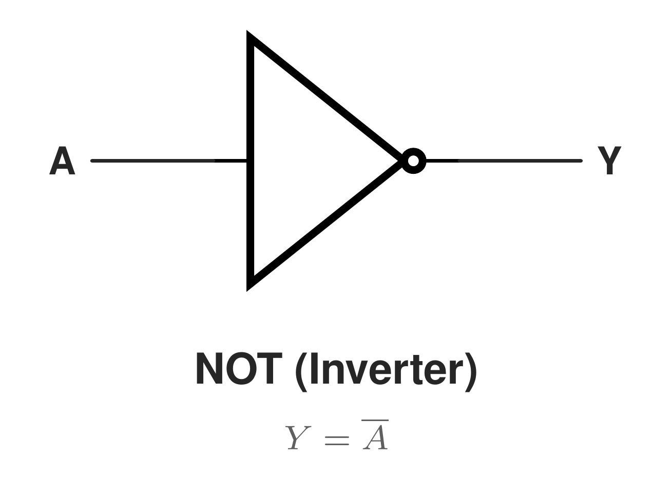
Figure: NOT gate symbol
| A | Y |
|---|---|
| 0 | 1 |
| 1 | 0 |
Table: NOT gate truth table.
Boolean expression: Y = A'
In practice: An inverter turns an active-low flag, such as `nRESET,` into an active-high signal that a GPIO can read.
#4 NAND Gate Symbol
A NAND gate drives its output LOW only when every input is HIGH. Its symbol is the AND shape with an output bubble, and it is the most widely stocked gate of all.
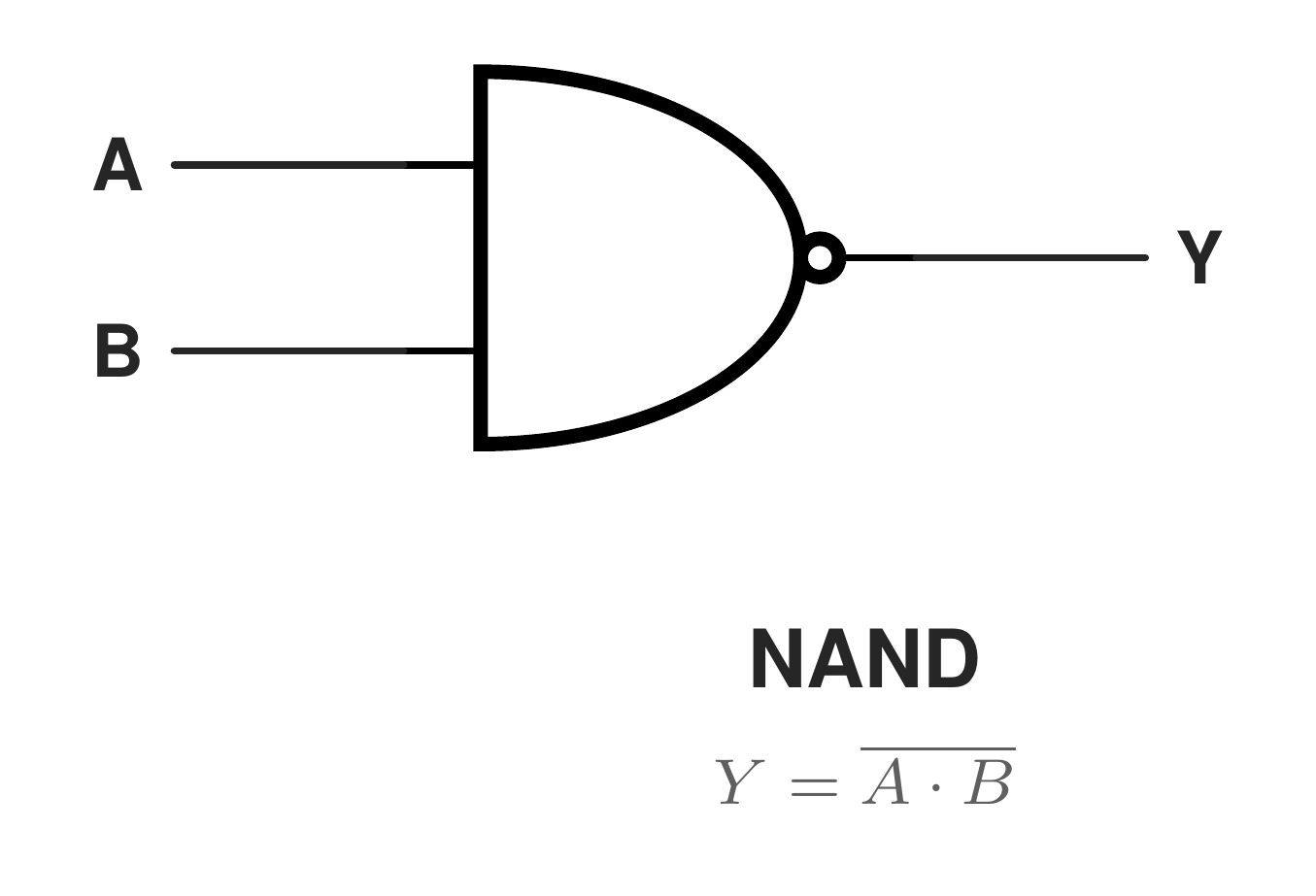
Figure: NAND gate symbol
| A | B | Y |
|---|---|---|
| 0 | 0 | 1 |
| 0 | 1 | 1 |
| 1 | 0 | 1 |
| 1 | 1 | 0 |
Table: NAND gate truth table.
Boolean expression: Y = (A · B)'
In practice: Two cross-coupled NAND gates form an SR latch, the classic debounce for a mechanical switch.
#5 NOR Gate Symbol
A NOR gate drives its output HIGH only when every input is LOW. Its symbol is the OR shape with an output bubble, and it is the second universal gate.
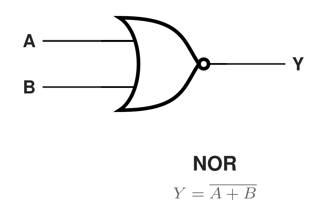
Figure: NOR gate symbol
| A | B | Y |
|---|---|---|
| 0 | 0 | 1 |
| 0 | 1 | 0 |
| 1 | 0 | 0 |
| 1 | 1 | 0 |
Table: NOR gate truth table.
Boolean expression: Y = (A + B)'
In practice: A NOR gate holds a reset asserted until every active-high power-good line has settled.
#6 XOR Gate Symbol
An XOR gate drives its output HIGH when its two inputs differ. Its ANSI symbol adds a second curved line across the input side of the OR shape.
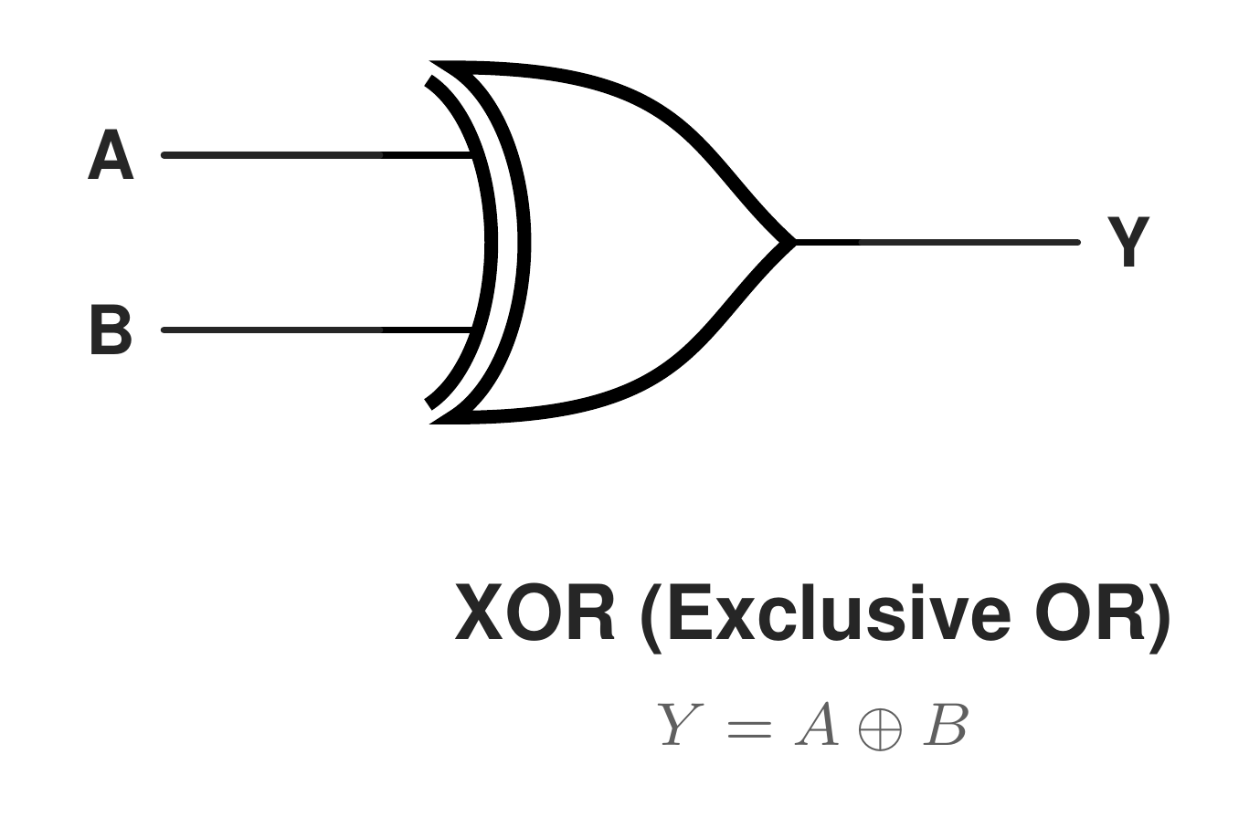
Figure: XOR gate symbol
| A | B | Y |
|---|---|---|
| 0 | 0 | 0 |
| 0 | 1 | 1 |
| 1 | 0 | 1 |
| 1 | 1 | 0 |
Table: XOR gate truth table.
Boolean expression: Y = A ⊕ B = A · B' + A' · B
In practice: An XOR gate produces the sum bit of a half adder. Tying one input HIGH turns it into a controlled inverter.
#7 XNOR Gate Symbol
An XNOR gate drives its output HIGH when its two inputs match. Its symbol is the XOR shape with an output bubble, so it is also called an equivalence gate.
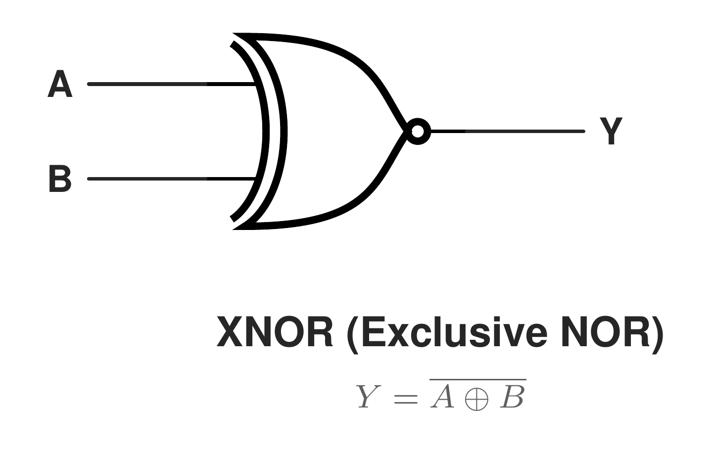
Figure: XNOR gate symbol
| A | B | Y |
|---|---|---|
| 0 | 0 | 1 |
| 0 | 1 | 0 |
| 1 | 0 | 0 |
| 1 | 1 | 1 |
Table: XNOR gate truth table.
Boolean expression: Y = (A ⊕ B)' = A · B + A' · B'
In practice: XNOR gates build the bit comparators in address decoders, where every bit must match.
#8 Buffer Gate Symbol
A buffer passes its input straight through. The symbol is a plain triangle with no bubble, and it exists to restore drive strength rather than to change the logic.
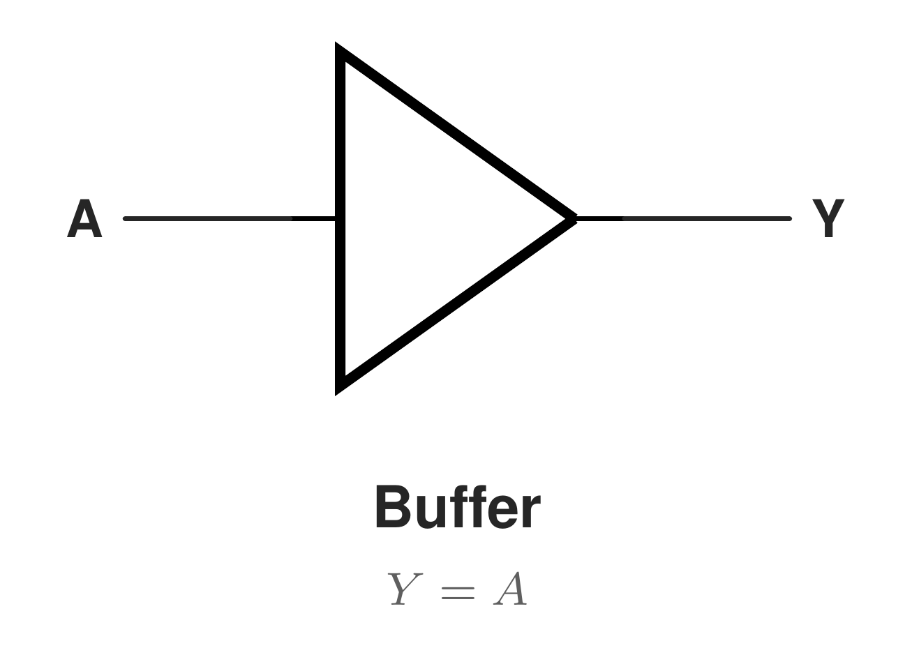
Figure: Buffer gate symbol
| A | Y |
|---|---|
| 0 | 0 |
| 1 | 1 |
Table: Buffer truth table.
Boolean expression: Y = A
In practice: A buffer restores edge rate on a long trace. The CD4050B also accepts inputs above its own supply, making it a simple down-level shifter.
ANSI/IEEE vs IEC Logic Gate Symbols: Key Differences
ANSI/IEEE Std 91-1984 uses distinctive gate outlines where the shape itself identifies the basic logic function.
IEC 60617-12 represents logic functions using rectangular symbols with standardized qualifying symbols inside.
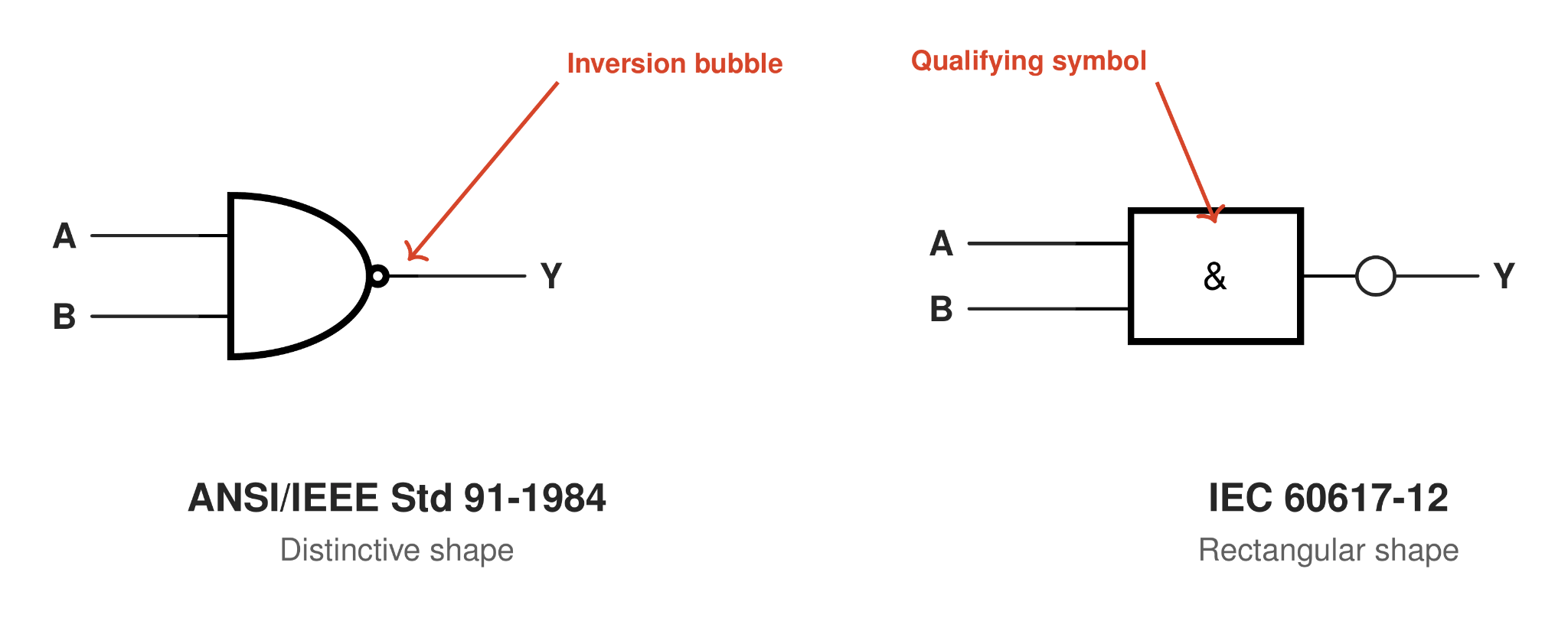
Figure: NAND gate drawn in ANSI and IEC form
| Attribute | ANSI/IEEE Distinctive Shape | IEC Rectangular Shape |
|---|---|---|
| Governing standard | ANSI/IEEE Std 91-1984, supplement 91a-1991 | IEC 60617-12, binary logic elements |
| Outline | A unique shape per function | Standardized rectangular block with function qualifiers |
| Function identifier | The shape itself | Qualifying symbol: &, ≥1, =1, or 1 |
| Inversion shown by | Small circle on the pin | Small circle, or a right-triangle wedge |
| More inputs | Additional input pins are added to the gate shape | Additional input pins are added to the rectangular block |
| Common in | US datasheets, default ECAD libraries | IEC-aligned drawings, European textbooks |
| Best at | Fast visual scanning of dense logic | Documenting multi-function blocks |
How to Read the Inversion Bubble on Any Gate Symbol
The small circle on a gate symbol is a negation indicator. On an output, it inverts the result. On an input, it indicates an active-low input, meaning the gate interprets that pin using the opposite logic level.
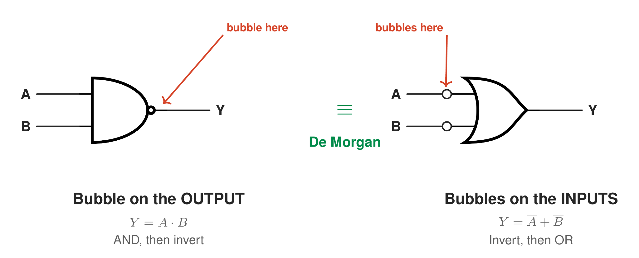
Figure: Inversion bubble anatomy comparing a bubble on the output
- Bubble on the output: The function is complemented. AND becomes NAND, OR becomes NOR, and XOR becomes XNOR.
- Bubble on an input: That pin is active LOW. The gate sees the inverted net.
- No bubble at all: The symbol is the plain function: AND, OR, XOR or buffer.
- Wedge instead of a circle: A polarity indicator under direct-polarity notation. It marks an active-LOW pin without inverting the logic function.
- Bubble facing bubble: Two negations on one net cancel, so the pair acts as a direct connection.
Universal Gates: Building Any Function From NAND or NOR
NAND and NOR are universal gates because either one alone can build every other logic function. That property, called functional completeness, lets a board use one part number instead of four.
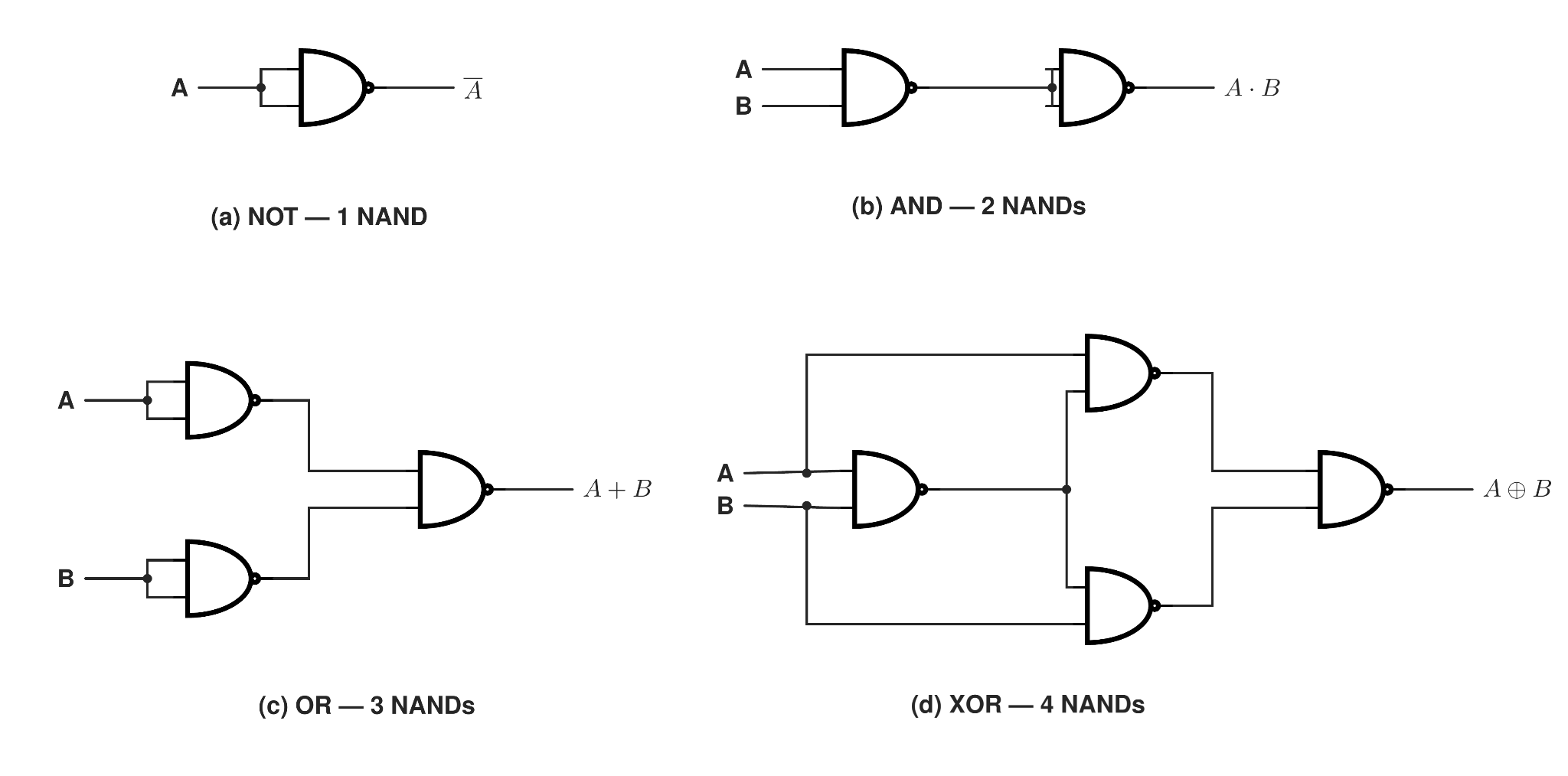
Figure: NAND-only construction of NOT, AND, OR and XOR
| Target Function | Built From NAND Gates | NANDs | Built From NOR Gates | NORs |
|---|---|---|---|---|
| NOT | Tie both inputs together | 1 | Tie both inputs together | 1 |
| AND | NAND, then a NAND inverter | 2 | Invert both inputs, then NOR | 3 |
| OR | Invert both inputs, then NAND | 3 | NOR, then a NOR inverter | 2 |
| NAND | Direct | 1 | Build AND, then invert | 4 |
| NOR | Build OR, then invert | 4 | Direct | 1 |
| XOR | Standard four-gate network | 4 | Five-gate network | 5 |
| XNOR | Five-gate network | 5 | Standard four-gate network | 4 |
Table: Gate count for building each function from NAND only or NOR only.
Logic Gate Symbols to 74xx and 4000-Series ICs: Pinout Reference
Each gate symbol maps to a real part number. Pick the family from your rail voltage first: 74HC runs on 2 V to 6 V, while the 4000B series runs on 3 V to 18 V.
| Gate | 74HC Part | 4000-Series Part | Gates per Package | Inputs per Gate |
|---|---|---|---|---|
| AND | 74HC08 | CD4081B | 4 | 2 |
| OR | 74HC32 | CD4071B | 4 | 2 |
| NOT | 74HC04 | CD4069UB | 6 | 1 |
| NAND | 74HC00 | CD4011B | 4 | 2 |
| NOR | 74HC02 | CD4001B | 4 | 2 |
| XOR | 74HC86 | CD4070B | 4 | 2 |
| XNOR | 74HC7266 | CD4077B | 4 | 2 |
| Buffer | 74HC4050 | CD4050B | 6 | 1 |
Table: Part lookup mapping each logic gate symbol to 74HC and 4000-series devices.
Note
Every device above ships in DIP-14, SOIC-14 and TSSOP-14, except the hex buffers, which are 16-pin parts.
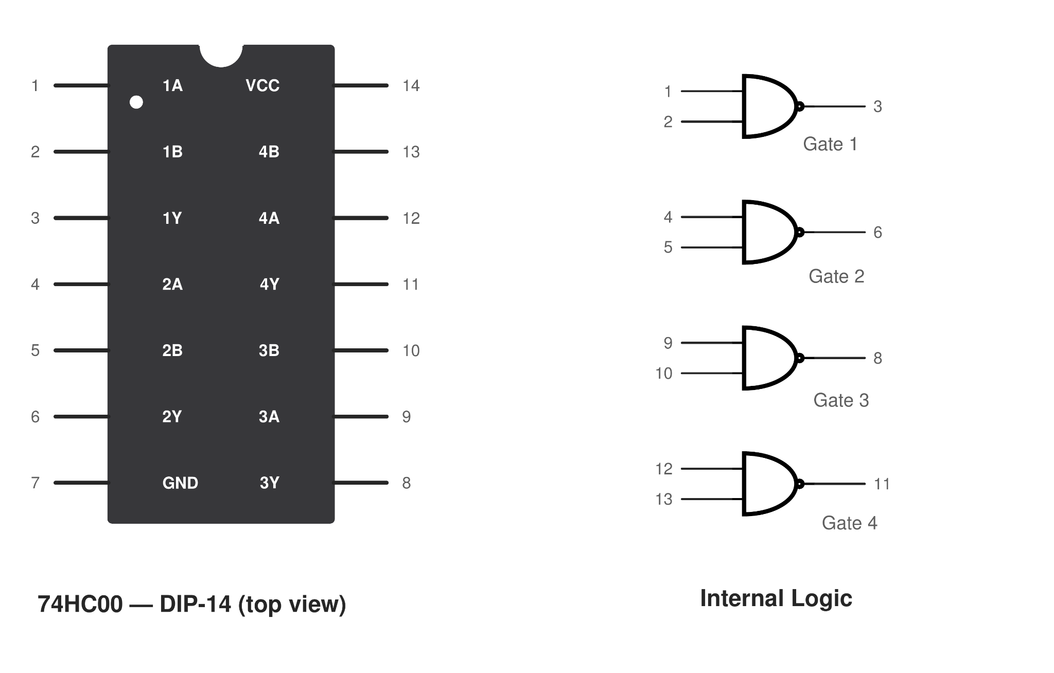
Figure: 74HC00 DIP-14 and SOIC-14 pinout with the four internal NAND gates
| Pin | Function | Pin | Function |
|---|---|---|---|
| 1 | 1A input | 14 | VCC |
| 2 | 1B input | 13 | 4B input |
| 3 | 1Y output | 12 | 4A input |
| 4 | 2A input | 11 | 4Y output |
| 5 | 2B input | 10 | 3B input |
| 6 | 2Y output | 9 | 3A input |
| 7 | GND | 8 | 3Y output |
Table: 74HC00 quad 2-input NAND pinout, 14-pin package.
At the transistor level, a 2-input CMOS NAND gate uses four MOSFETs: two PMOS transistors connected in parallel as the pull-up network and two NMOS transistors connected in series as the pull-down network. For a deeper look at the devices behind CMOS logic, see our MOSFET symbol guide and transistor symbol guide.

Check real-time availability and pricing for the logic ICs mentioned above in the JLCPCB Parts Library.
After completing your schematic and PCB design, upload your files to JLCPCB for an instant quote on PCB fabrication and assembly.
Conclusion
A logic gate symbol answers three questions at once. The shape names the function, the bubble names the polarity, and the pin numbers name the physical package. The third answer is the one that designers get wrong. Four gates share one package, one supply pin and one decoupling capacitor, so gate-level logic never maps one-to-one onto board-level layout.
Download the JLCPCB circuit symbols cheat sheet (PDF) for resistors, capacitors, diodes and transistors.
Keep learning:
FAQs about Logic Gate Symbols
Why Are There Two Sets of Logic Gate Symbols?
Two standards grew up in parallel. The distinctive shapes came from MIL-STD-806 and passed into ANSI/IEEE Std 91-1984, while IEC 60617-12 standardized the rectangle. Both are still valid, so datasheets use either.
What Are the 7 Basic Logic Gates?
The seven basic logic gates are AND, OR, NOT, NAND, NOR, XOR and XNOR. AND, OR and NOT are the primitives. NAND and NOR are universal, and XOR and XNOR compare two inputs.
What Is the Difference Between IEC and ANSI Logic Gate Symbols?
ANSI symbols name the function by outline shape, so you read them at a glance. IEC symbols use one rectangle per gate with a qualifier inside: & for AND, ≥1 for OR, and =1 for XOR.
Why Are NAND and NOR Called Universal Gates?
NAND and NOR are functionally complete, so either one alone can build every other function. Tying both inputs of a NAND together makes an inverter, and NAND networks then give AND, OR, NOR, XOR and XNOR.
Which IC Contains AND Gates?
The 74HC08 holds four two-input AND gates in a 14-pin package, and the CD4081B is its 4000-series equivalent for supplies to 18 V. The single-gate 74LVC1G08 fits a 5-pin SOT-353.
Popular Articles
• The Ultimate Guide to Relay Symbol: Coil, Contacts, Diagrams, and Circuit Applications
• Logic Gate Symbols: The Complete Chart, Truth Tables [2026]
• How to Design and Assemble a Reliable ESP32 Module PCB on a 2-Layer Board
• How to Identify SMD LED Polarity: Markings, Testing, and PCB Tips
• Power Supply Symbols Chart: A Complete Guide to AC, DC, Ground, Battery, and Source Symbols
Keep Learning
The Ultimate Guide to Relay Symbol: Coil, Contacts, Diagrams, and Circuit Applications
Think of a standard switch as a drawbridge you lift by hand. Now, imagine a relay symbol diagram as a remote-controlled drawbridge. It allows a tiny, low-power electronic signal to control a high-power electrical load from a distance safely. Understanding how to read relay symbol configurations is the absolute cornerstone of advanced circuit design. By mastering this relay schematic symbol, you move beyond basic electronics and enter the world of professional hardware logic and safe PCB design. What Y......
How to Read Resistor Color Code: Complete Guide with Chart and Examples
4-Band Resistor Color Code Explained A 4-band resistor color code is one of the most common methods used to indicate resistance values in electronic components. It is widely used to help engineers and hobbyists quickly determine resistance values without using a resistor color code calculator. In a standard 4-band resistor: First Band (Digit 1): Represents the first significant digit Second Band (Digit 2): Represents the second significant digit Third Band (Multiplier): Indicates the factor by which t......
Solder Paste vs Flux: What's the Difference and When Should You Use Each?
Solder paste and flux are not interchangeable. Solder paste contains solder alloy powder and flux, while flux contains no solder alloy. This difference matters when choosing materials for SMT, reflow soldering, or manual soldering. Flux removes metal oxides and prevents re-oxidation, allowing molten solder to wet copper pads and component leads properly. Solder paste combines flux with fine solder alloy powder. During reflow, the flux activates to improve wetting while the solder alloy melts to form t......
Fiducial Marks in PCB and SMT Assembly: A Complete Guide to Accuracy and Design Rules
Modern Printed Circuit Boards (PCBs) are complex, integrating high-density components like 0.4mm pitch Ball Grid Arrays (BGAs), 0201 passives, and fine-pitch Quad Flat No-Lead (QFN) packages. In this advanced manufacturing environment, achieving placement accuracy measured in micrometers is crucial. A significant challenge in automated manufacturing is how pick-and-place machines, which handle thousands of components per hour, precisely locate the PCB. A board on a conveyor system is never in the perf......
Ground Symbols Explained: Earth, Chassis, Signal, Analog, Digital Ground & More
Key Takeaways ⬇ Download the Ground Symbol Cheat Sheet (PDF) Keep all six ground symbols and their standard numbers on one page for quick reference. Four IEC 60417 symbols: IEC 60417 defines symbol 5017 for earth, 5018 for functional earth, 5019 for protective earth, and 5020 for frame/chassis. Protective earth is safety-related: IEC 60417-5019 identifies the protective earth connection and is used for safety-related protective bonding. Signal ground uses a different convention: IEEE Std 315 defines t......
How to Choose an ESP32 Development Board: A Beginner-Friendly Guide
The leap from blinking a simple LED to building a cloud-connected smart home device is a thrilling milestone for any electronics beginner. At the heart of this transition is often one undisputed champion: the ESP32. However, when you first search for an ESP32 development board, you are instantly met with a dizzying array of models, shapes, and specifications. How do you know which one is right for your first IoT (Internet of Things) project? In this beginner's guide, we will break down what makes thes......