
The Ultimate Guide to Relay Symbol: Coil, Contacts, Diagrams, and Circuit Applications
14 min
- What Does a Relay Symbol Represent in Circuit Diagrams?
- Anatomy of a Relay Symbol: Coils and Contact Terminals
- Types of Relay Symbols
- Normally Open (NO) vs Normally Closed (NC) Relay Symbols
- How to Read a Relay Symbol in a Circuit
- Best Practices for Drawing Relay Symbols
- Relay Symbol Examples in Real Circuits
- Relay Schematic Symbol vs Other Switch Symbols
- How to Map a Relay Symbol to a PCB Footprint
- PCB Layout Guidelines for Relay Circuits
- Common PCB Design Mistakes When Using Relay Symbols
- Relay PCB Assembly and Manufacturing with JLCPCB
- FAQs About Relay Symbol
- Conclusion
Think of a standard switch as a drawbridge you lift by hand. Now, imagine a relay symbol diagram as a remote-controlled drawbridge. It allows a tiny, low-power electronic signal to control a high-power electrical load from a distance safely.
Understanding how to read relay symbol configurations is the absolute cornerstone of advanced circuit design. By mastering this relay schematic symbol, you move beyond basic electronics and enter the world of professional hardware logic and safe PCB design.
What You Will Learn in this Guide:
1. Understand relay symbol meaning in circuit diagrams
2. Identify coil, COM, NO, NC terminals
3. Learn different relay symbol types (SPST, SPDT, DPDT, SSR)
4. Distinguish between IEC and ANSI symbol standards
5. Read relay symbols step-by-step
6. Map relay symbol to PCB footprint
7. Avoid common PCB design mistakes (trace widths, creepage)
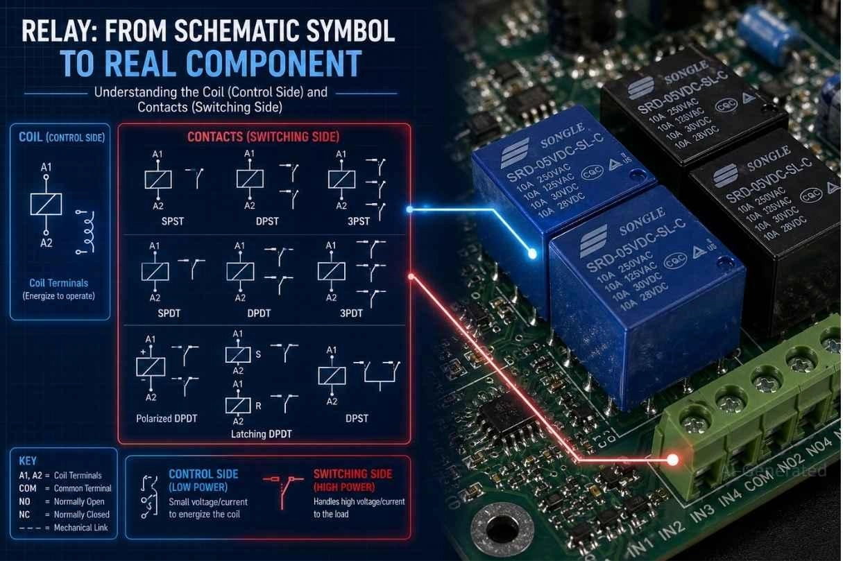
Figure: Illustrating the transition from a relay schematic symbol diagram to real physical relay components mounted on a PCB.
What Does a Relay Symbol Represent in Circuit Diagrams?
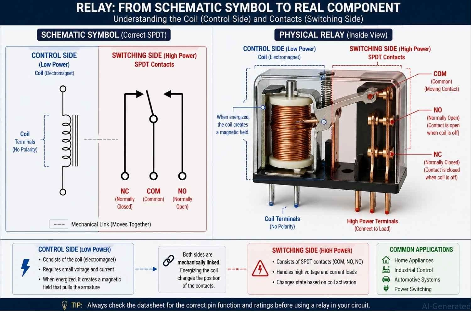
Figure: Diagram showing how a relay symbol represents both the low-power coil control side and the high-power contact switching side of a coil-driven switch.
| Part | Function |
|---|---|
| Coil | Control input |
| COM | Common terminal |
| NO | Open by default |
| NC | Closed by default |
The Relay Symbol as an Electrically Controlled Switch
At its core, a relay is an electrically controlled switch. The symbol is visually split into two distinct halves: the control side and the switching side.
The control side features the relay coil. The switching side features the physical metal contacts that open or close the circuit.
Relay Schematic Symbol vs Physical PCB Layout
A relay schematic symbol represents a logical function, not a physical shape. In a schematic diagram, the coil and the contacts might be drawn far apart for readability.
However, in the real hardware, they are housed inside the same physical plastic box. Understanding the distinction between this relay schematic and the PCB layout is vital for CAD design.
Electrical Isolation in Relay Symbol Diagrams
The most important feature of any relay is isolation. Notice that in a standard relay symbol diagram, the coil lines never touch the contact lines.
This visual gap represents physical galvanic isolation. It allows a delicate 5V microcontroller on the control side to safely switch a 240V mains appliance on the switching side without damaging your logic board.
Anatomy of a Relay Symbol: Coils and Contact Terminals
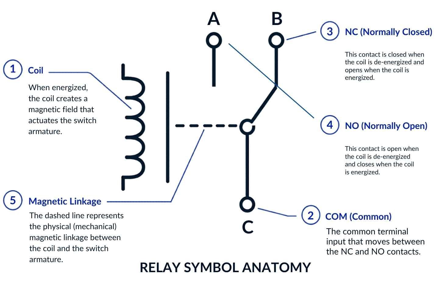
Figure: Detailed anatomy of a relay symbol showing the coil, COM, NO, and NC terminals, connected by a mechanical dashed line.
Relay Coil Symbol Variations (IEC vs ANSI Standards)
The relay coil symbol representation depends on the drafting standard:
- IEC 60617 Standard: Typically drawn as a rectangle.
- ANSI/IEEE 315 Standard: Typically drawn as a squiggly inductor line.
In modern schematics, these coils are almost always labeled with specific designators like K1, K2, or RL1 to help you track them on the Bill of Materials (BOM).
Relay COM, NO, and NC Terminals Explained
The switching side of the symbol is defined by three critical COM NO NC terminals:
- COM (Common): The main input line where power enters the switching side.
- NO (Normally Open Contact): The output path that remains disconnected until the relay is powered.
- NC (Normally Closed Contact): The output path that remains connected while the relay is unpowered.
Mechanical Linkage in Relay Symbol Diagrams
Look closely at the relay symbol diagram. You will often see a dashed line connecting the coil to the switch lever (armature).
This dashed line represents the physical linkage. It tells the engineer: "When this specific coil generates a magnetic field, it physically pulls this specific lever."
Types of Relay Symbols
The most common types of relay symbols used in circuit diagrams include:
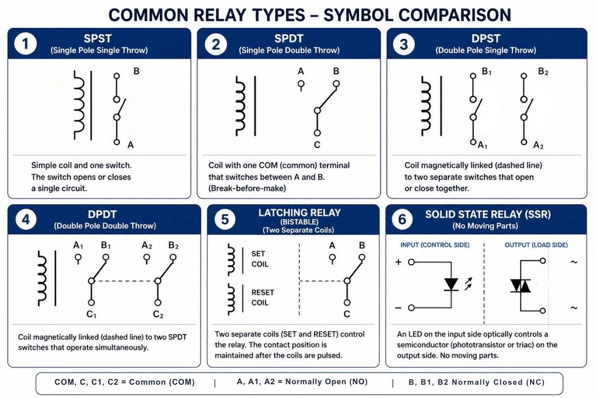
Figure: Different relay symbol types including SPST, SPDT, DPST, DPDT, Latching, and Solid State Relays (SSR).
SPST Relay Symbol (Single Pole Single Throw)
The Single Pole Single Throw (SPST) symbol is the simplest version. It features a coil and a basic ON/OFF switch.
It is used strictly for making or breaking a single high-power circuit path.
SPDT Relay Symbol (Single Pole Double Throw)
The SPDT relay symbol (Single Pole Double Throw) is the undisputed industry standard. It takes one common input and lets the coil toggle it between two separate outputs (NO and NC).
Understanding the SPDT relay symbol meaning is crucial because it allows for "changeover" switching logic - turning one device off while simultaneously turning another on.
DPST Relay Symbol (Double Pole Single Throw)
A Double Pole Single Throw (DPST) symbol represents two independent SPST switches that are mechanically linked and operated by a single coil.
It is frequently used for safety-critical applications, such as completely isolating both the live and neutral wires of an AC mains load simultaneously.
DPDT Relay Symbol (Double Pole Double Throw)
A Double Pole Double Throw (DPDT) symbol looks like two SPDT switches placed side-by-side.
A dashed line connects both levers to a single coil, meaning one electrical signal controls two completely independent switching circuits simultaneously.
Latching Relay Symbol (Bistable & Monostable)
A latching relay symbol represents a relay that mechanically retains its state even after power is removed, making it highly energy-efficient.
- Bistable: Often drawn with two distinct coils (a "set" coil and a "reset" coil).
- Monostable (Pulse Reversal): Uses a single coil where the polarity of the pulse determines the state.
Solid State Relay Symbol (SSR)
A Solid State Relay (SSR) symbol abandons the mechanical lever entirely. Because it has no moving parts, it represents extreme switching speed and durability.
Instead of a magnetic coil, the symbol usually depicts an internal LED (optocoupler) transmitting light across a gap to trigger a heavy-duty semiconductor.
- AC Loads: The output is typically a TRIAC.
- DC Loads: The output is typically a MOSFET.
Warning: AC-output SSRs (TRIAC) do not work with DC loads. Always match SSR type to your load. Using the wrong type will result in a non-functional or damaged circuit.
Normally Open (NO) vs Normally Closed (NC) Relay Symbols
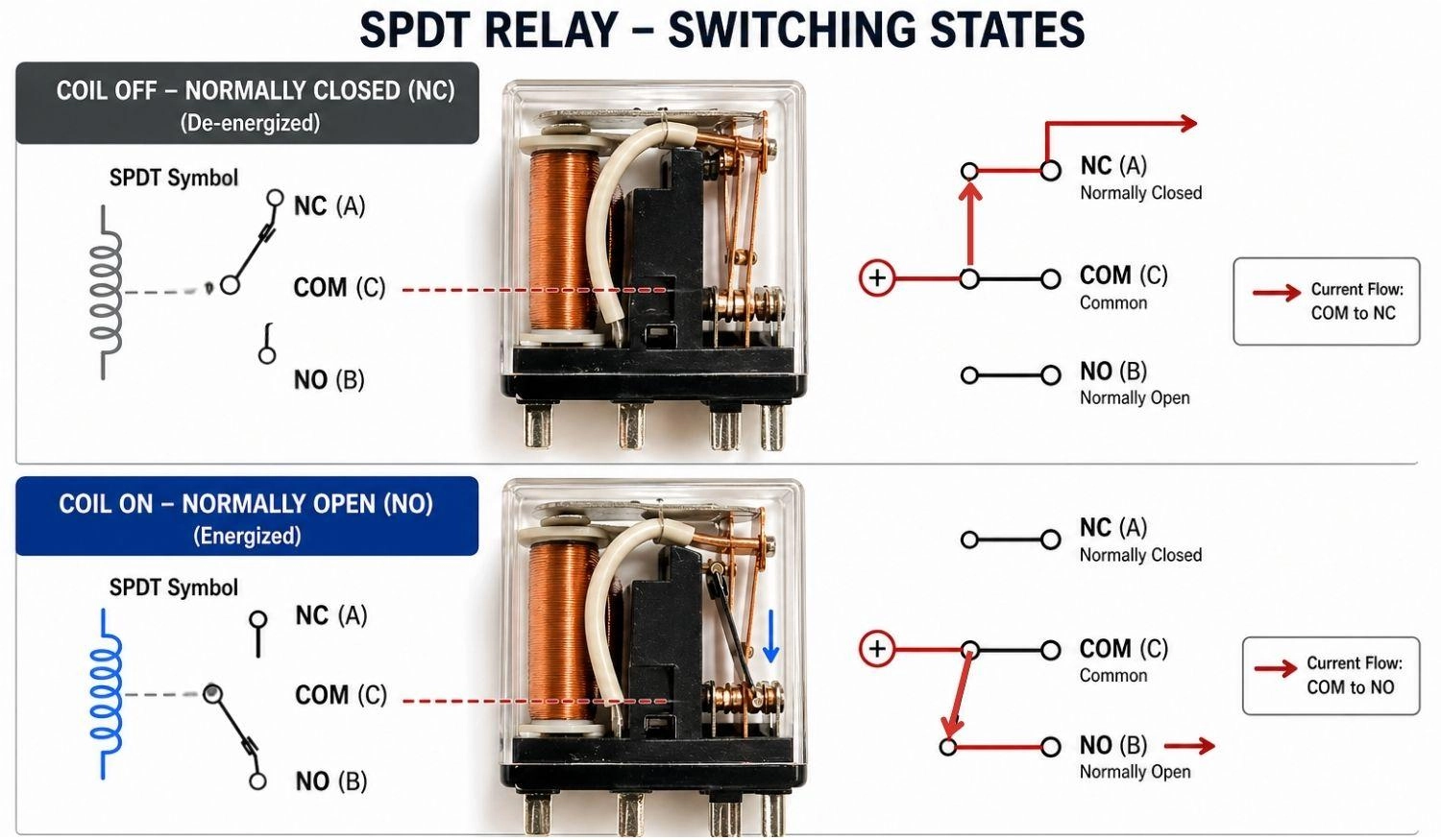
Figure: Diagram demonstrating the current flow in an SPDT relay during the Coil OFF (Normally Closed) and Coil ON (Normally Open) states.
Note
"Normally" refers to the relay's state when unpowered - not when your circuit is running.
How a Normally Open (NO) Relay Symbol Works
In a relay schematic symbol, the Normally Open (NO) contact is shown with a gap between the moving contact and the terminal.
The circuit remains open (no current flows) when the coil is de-energized, and it closes (conducts) when the coil is energized.
How a Normally Closed (NC) Relay Symbol Works
The Normally Closed (NC) contact is drawn with the moving contact touching the terminal.
The circuit remains closed (current flows) when the coil is de-energized, and it opens when the coil is energized.
NO/NC Relay State Switching Table
| Relay State | Coil OFF (Unpowered) | Coil ON (Energized) |
|---|---|---|
| NO Terminal | Open (No current) | Closed (Current flows) |
| NC Terminal | Closed (Current flows) | Open (No current) |
How to Read a Relay Symbol in a Circuit
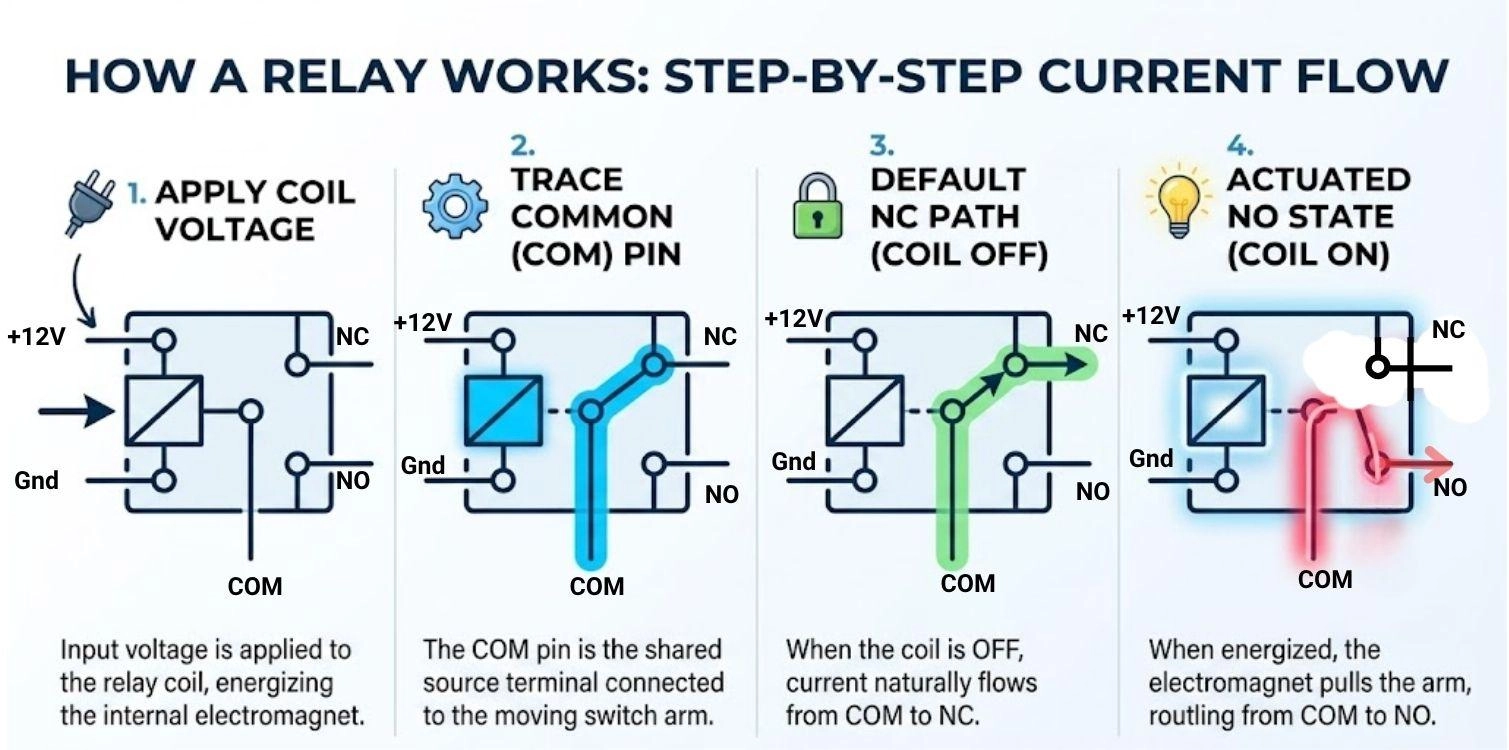
Figure: A step-by-step visual guide on how to read a relay symbol and trace its internal current flow.
Mastering how to read relay symbol diagrams prevents wiring errors. Follow this strict sequence:
Step 1: Identify coil terminals
Locate the control pins (often A1/A2 or pins 1/2) that energize the electromagnet.
Step 2: Locate COM terminal
Find the main common input where your high-power voltage enters the switching side.
Step 3: Identify NO and NC
Note which terminal is connected by default (NC) and which requires power to connect (NO).
Step 4: Trace switching path
Follow the logical current flow for both the "unpowered" and "powered" states to verify your circuit logic.
Best Practices for Drawing Relay Symbols
- Always verify the datasheet before finalizing your footprint mapping.
- Label relays clearly on your schematic using standardized designators like K1, K2, or RL1.
- Use standard, verified libraries in your PCB software to prevent pinout errors.
- Include protection circuits (snubbers or flyback diodes) directly adjacent to the relay symbol.
Relay Symbol Examples in Real Circuits
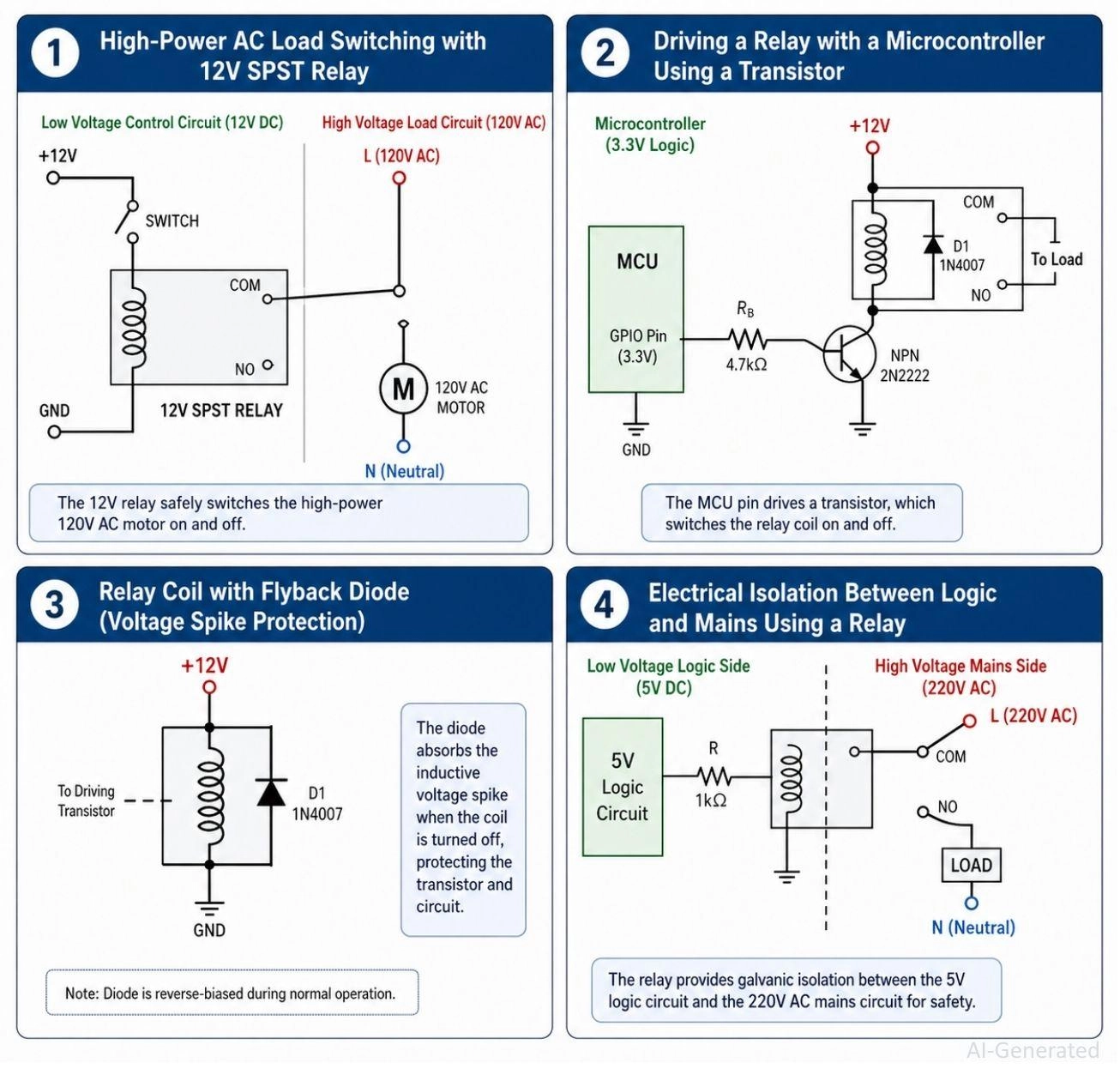
Figure: Four practical circuit diagram examples showing a motor relay, a microcontroller relay driver, a flyback diode protection circuit, and an isolation barrier.
SPST Relay Symbol Driving a Motor Load
- Used for high power switching.
- A tiny dashboard switch sends 12V to the coil, which closes the heavy-duty contacts to spin a massive starter motor.
Microcontroller Relay Coil Control Circuit
- An Arduino or ESP32 cannot output enough current to drive a coil directly.
- The schematic will show the microcontroller triggering an intermediate transistor, which then safely dumps power into the relay coil.
Relay Schematic Symbol with Flyback Diode Protection
- A vital protection circuit seen in professional schematics.
- A diode is placed in a reverse-bias orientation across the relay coil. When the electromagnet collapses, the reversed polarity forward-biases the diode, allowing it to safely absorb the massive voltage spike. Note that this diode can slightly slow the relay's release time, a factor to consider in timing-critical applications.
High-Voltage Isolation Using a Relay Symbol
- Demonstrates the transition from low voltage to high voltage.
- The symbol explicitly shows the physical gap separating a delicate 3.3V smart-home logic board from a 240V mains circuit.
Relay Schematic Symbol vs Other Switch Symbols
Understanding when to use a relay versus other switching components is critical. Here is a quick feature comparison:
| Feature | Switch | Relay | Transistor | SSR |
|---|---|---|---|---|
| Control | Manual | Coil | Base/Gate | Optical |
| Isolation | None | Full | None | Full |
| Speed | Slow | Medium | Fast | Very fast |
| Moving Parts | Yes | Yes | No | No |
| Use Case | User input | High power | Logic switching | Silent switching |
How to Map a Relay Symbol to a PCB Footprint
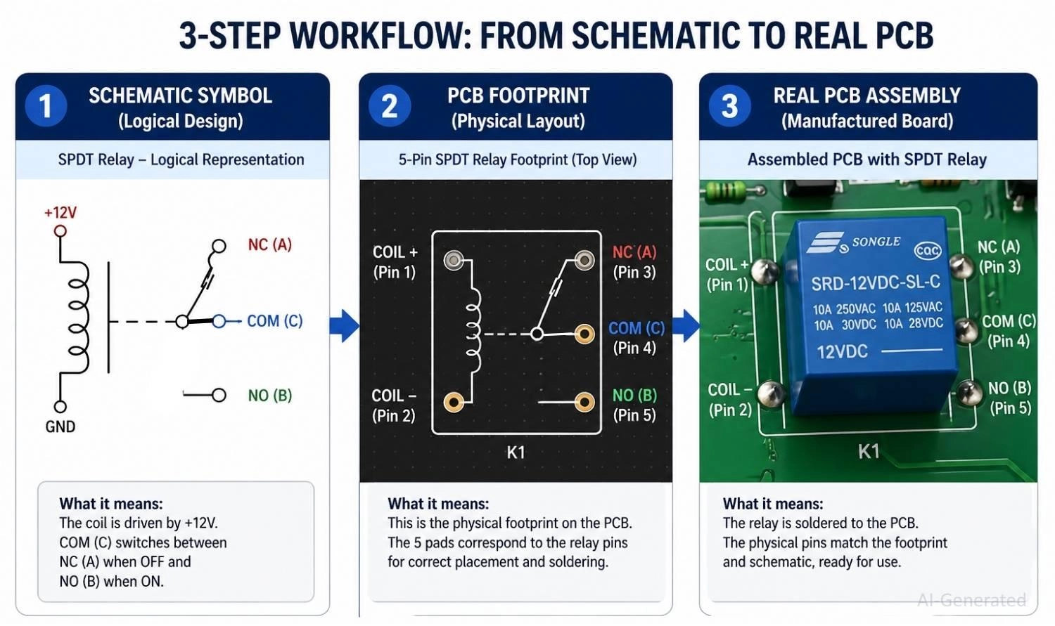
Figure: Workflow demonstrating the transition from a logical relay schematic symbol to a physical PCB footprint layout, ending with a real soldered component.
Logical Symbol vs Physical Footprint
Understanding the relay symbol in PCB design requires separating logic from reality.
The symbol is logical (arranging pins for easy reading). The footprint is physical (arranging copper pads to match the precise plastic dimensions of the real component).
5-Pin Relay Footprint Mapping Example (SRD-05VDC-SL-C)
Successfully integrating a relay schematic vs PCB layout requires strict discipline. Let's look at mapping a common 5-pin SPDT relay:
1. Read the Datasheet: The datasheet shows five physical pins. Two are for the coil, one is COM, one NO, and one NC.
2. Verify the Symbol: Ensure your schematic symbol has exactly 5 corresponding pins.
3. Assign the Footprint: Select the footprint matching the physical pin pitch (e.g., standard 2.54mm grid spacing for the coil pins, but wider spacing for the contact pins). Assigning the wrong footprint will result in a board that cannot be assembled.
PCB Layout Guidelines for Relay Circuits
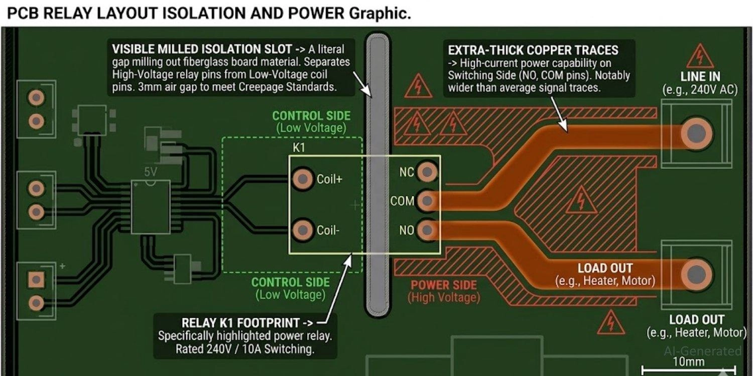
Figure: PCB layout graphic highlighting thick high-current traces and milled isolation slots around a relay footprint.
When routing relays on a PCB, strict adherence to design rules is required to prevent catastrophic failure or safety hazards.
| Design Rule | Standard | Key Requirement |
|---|---|---|
| Trace width | IPC-2221 | Size based on current |
| Creepage | IEC 62368 | ≥ 6mm for mains |
| EMI | — | Use snubber or flyback diode |
| Thermal | — | Use copper pour |
High Current Trace Routing in Relay Circuits (IPC-2221 Standard)
Because the switching contacts handle massive loads, the PCB traces connected to the COM, NO, and NC pins must be thick enough to prevent melting. Designers typically use the IPC-2221 standard to calculate minimum trace width based on the maximum current and allowable temperature rise (e.g., a rough rule of thumb is often ~1mm of trace width per Ampere for 1oz copper, but always calculate precisely).
Creepage and Clearance for Relay Isolation
To maintain safety, PCB designers must enforce strict safety spacing between the high-voltage and low-voltage traces. For mains applications (e.g., 240V), standards like IEC 60950 or IEC 62368 specify minimum creepage distances (often 6mm or more for reinforced insulation). Often, actual slots are routed out of the board to increase the creepage distance along the surface.
EMI and Switching Noise Mitigation
Opening and closing a physical contact creates electrical arcing and switching spikes. Poor layout will cause this Electromagnetic Interference (EMI) to reset your microcontrollers.
Thermal Relief for Relay Footprints
Both the energized coil and the high-current contacts generate heat. Ensure adequate copper pours around the relay footprint to act as a heatsink.
Common PCB Design Mistakes When Using Relay Symbols
- Confusing NO and NC: Wiring a heater to the NC pin, causing it to turn ON when the system crashes.
- Incorrect pin mapping: Failing to match the logical symbol pins to the physical footprint, making assembly impossible.
- Ignoring the datasheet: Assuming all 5-pin relays share the same standard pinout layout (they do not).
- Missing the flyback diode: Forgetting to add protection, resulting in destroyed driver transistors.
- Wrong footprint selection: Designing for a tiny signal relay when the circuit requires a massive power relay.
Relay PCB Assembly and Manufacturing with JLCPCB
Schematic Validation and Manufacturing Workflow
Turning your relay schematic symbol into a physical board requires a precise manufacturing workflow.
After completing schematic validation, you must generate a Bill of Materials (BOM) and a Component Placement List (CPL) file.
Use JLCPCB Parts Library to quickly verify the correct symbol-footprint pairing and avoid pin-mapping errors before layout.
PCB Assembly Considerations for Relays
When opting for automated assembly, consider relay size and weight. Heavy relays can face mechanical stress during shipping, requiring impeccable solder reliability.
Relay miswiring and incorrect footprint selection are common causes of PCB failure. Utilize JLCPCB's comprehensive Parts Library to find verified relay footprints (like the standard 5-pin THT footprint) and seamlessly integrate them into your design.
When you are ready, get an instant quote and upload your Gerbers via JLCPCB's PCB Assembly services to ensure your components are perfectly aligned and professionally soldered.

- Upload Gerber files to JLCPCB
- Select correct IC footprint
- Use PCB Assembly services
FAQs About Relay Symbol
Q: How do you read a relay symbol?
Locate the coil pins to find the control input, identify the COM input, and trace the path through the Normally Open (NO) or Normally Closed (NC) pins.
Q: What is an SPDT relay symbol?
Single Pole Double Throw. It takes one common input and uses the coil to toggle it between two separate output paths.
Q: What is NO vs NC in a relay?
Normally Open (NO) breaks the circuit when unpowered. Normally Closed (NC) connects the circuit when unpowered.
Q: Can I drive a relay directly from an Arduino?
It depends on the type. A standard bare relay coil draws too much current for a microcontroller pin, requiring a transistor or relay driver IC. However, you can use a pre-built logic-level relay module, which includes the necessary driver circuit and allows for a direct connection.
Q: Why does a standard relay have 5 pins?
Two pins are for the coil, and three are for the switching side: Common (COM), Normally Open (NO), and Normally Closed (NC).
Q: What is a flyback diode and why is it needed?
It is a diode placed in reverse-bias across the relay coil. It protects your driver circuit from the massive voltage spike generated when the coil's magnetic field collapses.
Q: What is the difference between IEC and ANSI relay symbols?
The IEC standard draws the relay coil as a rectangle, while the ANSI standard draws it as a squiggly inductor line.
Q: Does a relay symbol affect PCB design?
Absolutely. The logical symbol must be perfectly mapped to a physical footprint, ensuring proper trace widths and high-voltage isolation clearances on the real board.
Conclusion
The relay symbol is the ultimate bridge between delicate digital logic and massive physical power. Because relays enable safe switching, they are an absolute necessity in everything from smart home automation to industrial motor control.
By mastering how to read the SPDT relay symbol, tracing current through NO and NC contacts, and understanding the vital importance of electrical isolation, you can safely integrate complex power routing into your schematics. These symbols don't just represent parts; they represent the critical logic required for real, reliable PCB design.
Ready to safely control high power on your next board? Before ordering your PCB, verify relay pin mapping, footprint alignment, and isolation spacing-these are the most common causes of failure.
Popular Articles
• How to Create a Bluetooth-Controlled Car With Arduino: A Step-by-Step Guide
• How to Design and Assemble a Reliable ESP32 Module PCB on a 2-Layer Board
• The Ultimate Guide to Relay Symbol: Coil, Contacts, Diagrams, and Circuit Applications
• How to Identify SMD LED Polarity: Markings, Testing, and PCB Tips
• The Ultimate Guide to PCBA: Process,Types and Techniques for the Electronics Enthusiast
Keep Learning
How to Design an ESP32-S3 Development Board from Scratch: A 4-Layer PCB Design Tutorial
Designing your own ESP32-S3 development board gives you complete control over your hardware architecture while preparing your IoT projects for commercial production. Instead of relying on bulkier, off-the-shelf boards, building a custom design allows you to optimize the board space, expose only the required GPIO pins, and integrate peripherals directly onto a single substrate. In this tutorial, we will design a 4-layer ESP32-S3 development board from scratch. We will walk through the entire hardware d......
Arduino LED Driver Tutorial: Control More LEDs with 74HC595 and MAX7219
Arduino GPIO pins run out quickly in larger LED projects. By utilizing dedicated LED drivers and expansion ICs, you can drastically reduce pin usage, eliminate processor-heavy multiplexing loops, and simplify display wiring. In this guide, you will learn the operational architecture, wiring configurations, cascading techniques, and optimization strategies for the 74HC595 shift register and the MAX7219 LED driver. Why Arduino Projects Need LED Driver ICs Arduino GPIO and Current Limitations An ATmega32......
How to Create a Bluetooth-Controlled Car With Arduino: A Step-by-Step Guide
This tutorial walks through the complete engineering and implementation of a two-wheel Bluetooth RC car with an Arduino Nano module on a specially designed PCBA (Printed Circuit Board Assembly). While many hobbyists start by wiring motors and Bluetooth modules with jumper cables on a breadboard, this approach is prone to disconnection and signal noise. This guide upgrades that process by teaching you how to design a professional mainboard. Key Design Features Controller: Arduino Nano used as a plug-in......
Fiducial Marks in PCB and SMT Assembly: A Complete Guide to Accuracy and Design Rules
Modern Printed Circuit Boards (PCBs) are complex, integrating high-density components like 0.4mm pitch Ball Grid Arrays (BGAs), 0201 passives, and fine-pitch Quad Flat No-Lead (QFN) packages. In this advanced manufacturing environment, achieving placement accuracy measured in micrometers is crucial. A significant challenge in automated manufacturing is how pick-and-place machines, which handle thousands of components per hour, precisely locate the PCB. A board on a conveyor system is never in the perf......
Alternating Current vs Direct Current (AC vs DC): What's the Difference?
Electric current flows in two primary forms: alternating current (AC) and direct current (DC). AC periodically reverses direction, while DC flows steadily in one direction. AC powers the industrial and residential electrical grids, while DC powers batteries, electric vehicles, and nearly all modern consumer electronics. Understanding the core differences between AC and DC matters when designing power supplies, selecting electronic components, or laying out printed circuit boards (PCBs). This guide com......
Arduino LED Multiplexing Tutorial: Control More LEDs with Fewer Pins
The Arduino Uno is a powerful tool for prototyping, but driving multiple LEDs directly quickly exhausts its 20 GPIO pins and its 200 mA absolute maximum package current limit. To bypass these hardware bottlenecks, engineers and hobbyists use LED multiplexing to scale display outputs efficiently without upgrading the microcontroller. In this guide, you will learn the core principles of LED matrix scanning, Charlieplexing, refresh timing, ghosting fixes, and practical Arduino code without relying on any......