
How to Design and Assemble a Reliable ESP32 Module PCB on a 2-Layer Board
9 min
- Step 1 – Designing the ESP32 Module Schematic
- Step 2 – Laying Out a 2-Layer PCB for ESP32 Modules
- Step 3 – Designing the ESP32 Module PCB for SMT Assembly
- Step 4 – Preparing Gerber, BOM, and CPL Files for ESP32 Module SMT Assembly
- Step 5 – Ordering ESP32 Module PCBA at JLCPCB
- Managing Assembly Yield and Inspection Risks
- Bring-Up and Validation of the ESP32 Module PCBA
- Conclusion
- FAQs
Many engineers fail when designing their first ESP32 PCB due to antenna issues, power instability, or SMT defects.
Designing a custom board with an ESP32 Module strikes the perfect balance between customizability and ease of manufacturing. Unlike a chip-down design, the module integrates the crystal oscillator, flash memory, and RF matching network, reducing the PCBA risk significantly.
the SMD package (for example, ESP32-S2-WROOM modules) introduces several assembly considerations, including pad solder wicking, thermal management of the RF shield, and maintaining adequate antenna clearance during PCB assembly.
This guide shows how to design a reliable ESP32-S2 module PCB on a 2-layer board.
Step 1 – Designing the ESP32 Module Schematic
Using an ESP32 SMD module simplifies the BOM by eliminating external clocks and RF passives. From a PCBA standpoint, the schematic stage is where cost, sourcing stability, and assembly yield are determined.
1.1 Selecting Components for ESP32 Module Designs
Your schematic components must map to real inventory.
● Basic vs. Extended Parts: JLCPCB distinguishes between "Basic" parts (pre-loaded on feeders, no setup fee) and "Extended" parts (require manual loading, fee applies). To reduce the costs of PCBA, prioritize "Basic" resistors and capacitors of sizes 0603/0402.
● Availability Check: Before concluding with the schematic, check the availability of the ESP32-S2 module and important ICs (LDOs) in the JLCPCB parts library.
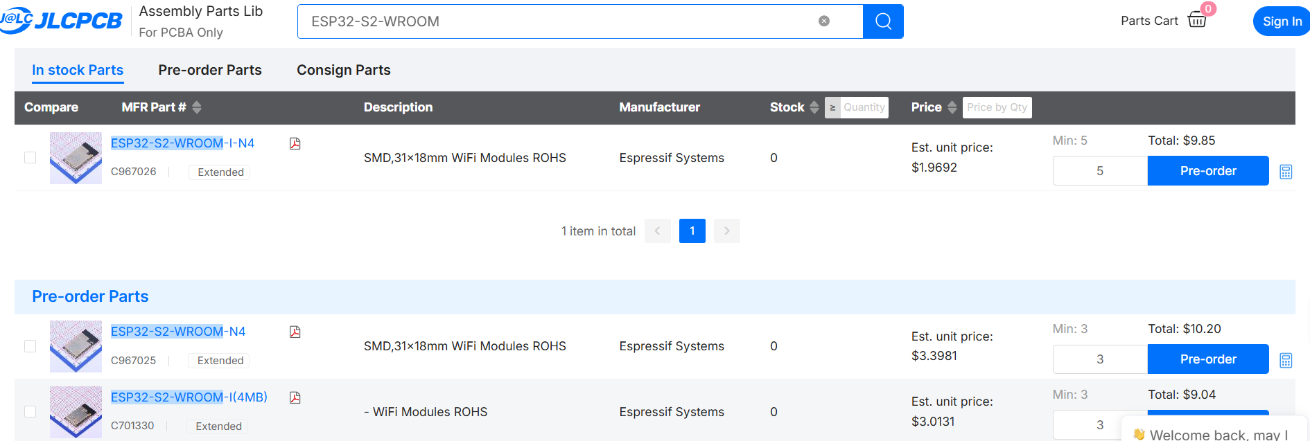
Figure: Searching ESP32-S2-WROOM in JLCPCB Parts Library
1.2 Understanding the ESP32-S2-Wroom Microcontroller Module
The module features 41 pins (castellated edges) and an integrated PCB antenna.
● Electrical Specs: A strong 3.3V rail that can handle 320mA (TX peaks) is required.
● PCBA Advantage: The internal 40MHz crystal is already shielded and matched, removing the most common cause of boot failures in custom boards.
1.3 Designing the UART Programming Interface (FTDI) for the Microcontroller
Bypassing the USB connector and bridge chip, an external FTDI adapter will be connected via a 2.54mm Pin Header.
● Connections: Route U0TXD (GPIO 43) and U0RXD (GPIO 44) to the connector header.
● Boot Strap Pins: Make the EN (Reset) pin available through tactile switches or the header so that manual entry into bootloader mode is possible.
Note
Please verify GPIO mapping against your specific ESP32-S2-WROOM datasheet.
1.4 Validating the Schematic for ESP32 Module PCBA
Before converting to PCB layout, perform these assembly-focused checks:
1. Pin Numbering: Does the schematic symbol pinout match the specific SMD-41P datasheet variant?
2. Net Connectivity: Are the strapping pins (GPIO 0, GPIO 46) pulled to the correct levels (Pull-up/Pull-down) to ensure the chip boots from flash?
3. Power Nets: Are the 3.3V and GND nets clearly defined and connected to all power pins (VDD3P3_RTC, VDD3P3_CPU)?
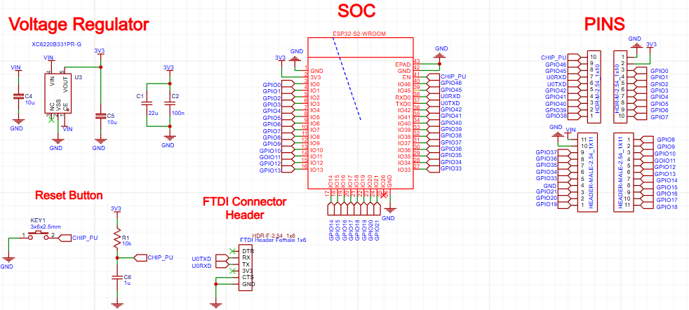
Figure: Schematic diagram of ESP32-S2 module with FTDI header and power circuit.
Step 2 – Laying Out a 2-Layer PCB for ESP32 Modules
It is necessary to follow the mechanical and thermal rules very carefully when designing a two-layer board for the ESP32 SMD module.
2.1 Designing Castellated Pads and the Thermal Pad
The module has a large central Ground pad (EPAD) under the metal shield (check your specific datasheet, as some SMD-41P variants have a full EPAD while others just use the pins).
● Via Layout: If your module has a central EPAD, place a 3x3 grid of 0.3mm vias connecting to the bottom Ground plane for heat dissipation.
● Castellated Pads: The pad on the PCB should be a bit longer than the pad of the module (extend it 0.5mm outwards) so that the solder fillet can form a visible "heel" for inspection.
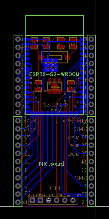
Figure: PCB footprint layout for ESP32-S2 showing castellated pad extension and antenna keep-out.
2.2 Implementing Proper Antenna Keep-Out for ESP32 PCB Antennas
The "On-board PCB Antenna" (the squiggly trace at the end of the module) is extremely sensitive.
● Placement: The best location is hanging off the edge of the board.
● Keep-Out: If the module is fully on the board, you must remove all copper (GND, Power, Signals) on all layers directly underneath the antenna area for at least 15mm. Copper underneath will detune the antenna and block the signal.
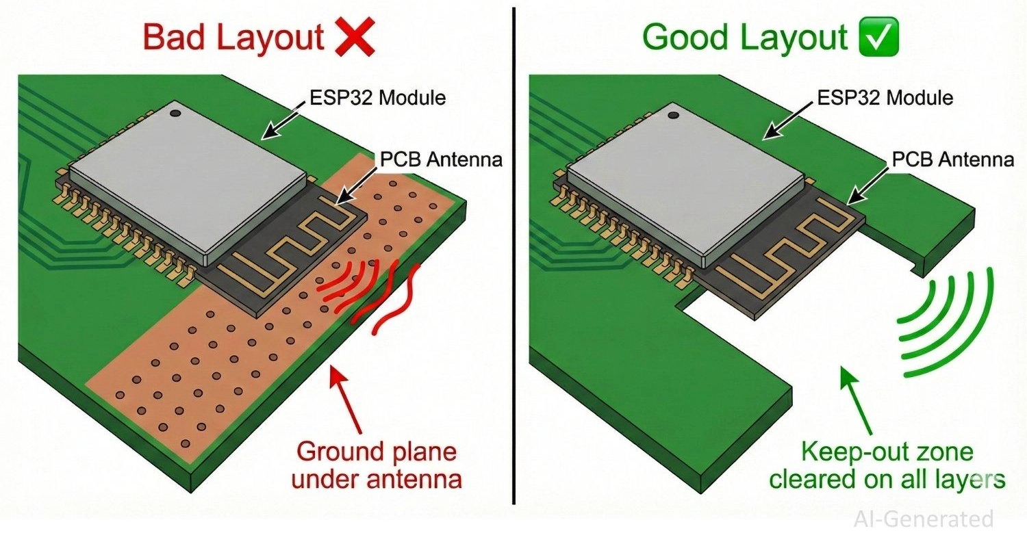
Figure: PCB layout comparison showing correct antenna keep-out zone vs incorrect ground plane placement for ESP32 modules.
2.3 Ensuring Power Integrity for ESP32 TX Current Peaks (320mA)
● Capacitor Layout: Place a 10uF (0603) and a 0.1uF (0402) capacitor close to the 3V3 input pin (Pin 2 on many SMD-41P pinouts).
● Trace Width: To reduce the voltage drop caused by the 320mA transmission spikes, the primary 3.3V trace should have a width of at least 20-30 mils.
Step 3 – Designing the ESP32 Module PCB for SMT Assembly
3.1 Designing the FTDI Header for SMT Assembly and Mechanical Reliability
Using a simple header simplifies the BOM but requires mechanical consideration.
Header DFM
● SMD Headers: The copper area of the pads must be large enough to accommodate the insertion force of the FTDI cable when using SMT headers.
● Pin Definition: Standardize your pinout (e.g., GND, CTS, VCC, TX, RX, DTR) to match common FTDI cables.
| Defect | Root Cause | Prevention |
|---|---|---|
| Insufficient Wicking | Pad too short | Extend PCB pad 0.5mm outside |
| Shadowing | Module blocks heat | Adjust Reflow Profile |
| Antenna Detuning | Copper under antenna | Strict Keep-Out Zone |
3.2 Optimizing Solder Paste and Stencil Apertures for ESP32 Modules
The large metal shield of the SMD-41P module acts as a heat sink, which affects how solder paste melts.
● Castellated Pins: The stencil aperture for the side pins should be 1:1 or slightly enlarged to ensure enough paste volume. The goal is to have the solder wick up the vertical side of the module.
● Thermal Pad (If present): Use a "Window Pane" design (50-60% coverage) to prevent the module from floating on a pool of solder, which would disconnect the outer pins.
3.3 Applying Design for Manufacturing (DFM) Rules for ESP32 Modules at JLCPCB
Component Spacing
Maintain at least 1.0mm clearance around the module. This allows the Pick-and-Place machine nozzle to place the module without hitting adjacent resistors or capacitors.
Check JLCPCB PCB Manufacturing & Assembly Capabilities for more details.
Panelization
For small boards, use the "Panel by JLCPCB" option.
Orientation: Ensure the USB/FTDI connector (if overhanging) or the antenna overhang does not interfere with the V-cut rails.
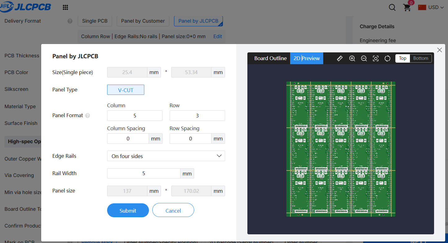
Figure: Panel by JLCPCB
Step 4 – Preparing Gerber, BOM, and CPL Files for ESP32 Module SMT Assembly
1. Gerber Files: Standard Gerber export in any eda software.
2. CPL Rotation: Verify the rotation of the large module in the JLCPCB 3D viewer. It is common for modules to be rotated 90 or 180 degrees incorrectly in the default export.
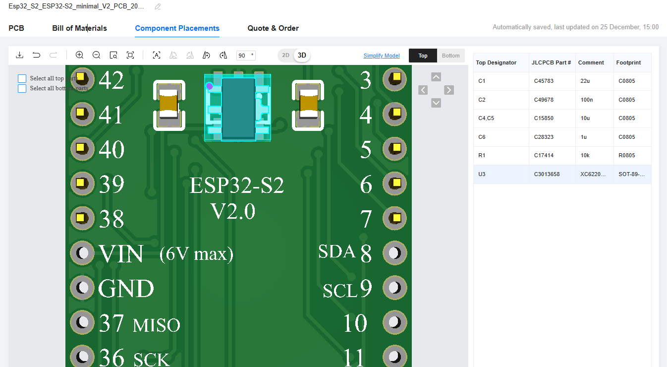
Figure: Component Placement 3d view showing an unaligned rotated component
Step 5 – Ordering ESP32 Module PCBA at JLCPCB
1. Uploading Gerber files and selecting SMT assembly services on the JLCPCB instant quote page.
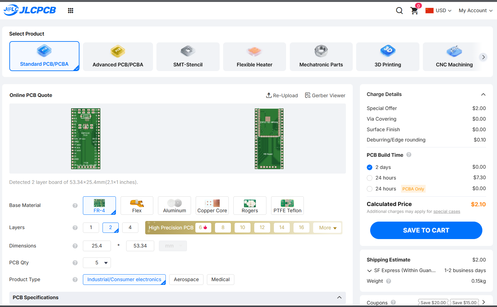
2. Select PCB Assembly and standard type for both sides
3. Sourcing: Check if the specific "ESP32-S2 SMD-41P" module is in the JLCPCB Parts Library. If it is an "Extended Part," you will pay a small loading fee (approx $3).
4. Global Source: If the part is not in the JLCPCB library, you can often source it via Global Sourcing during the order process.
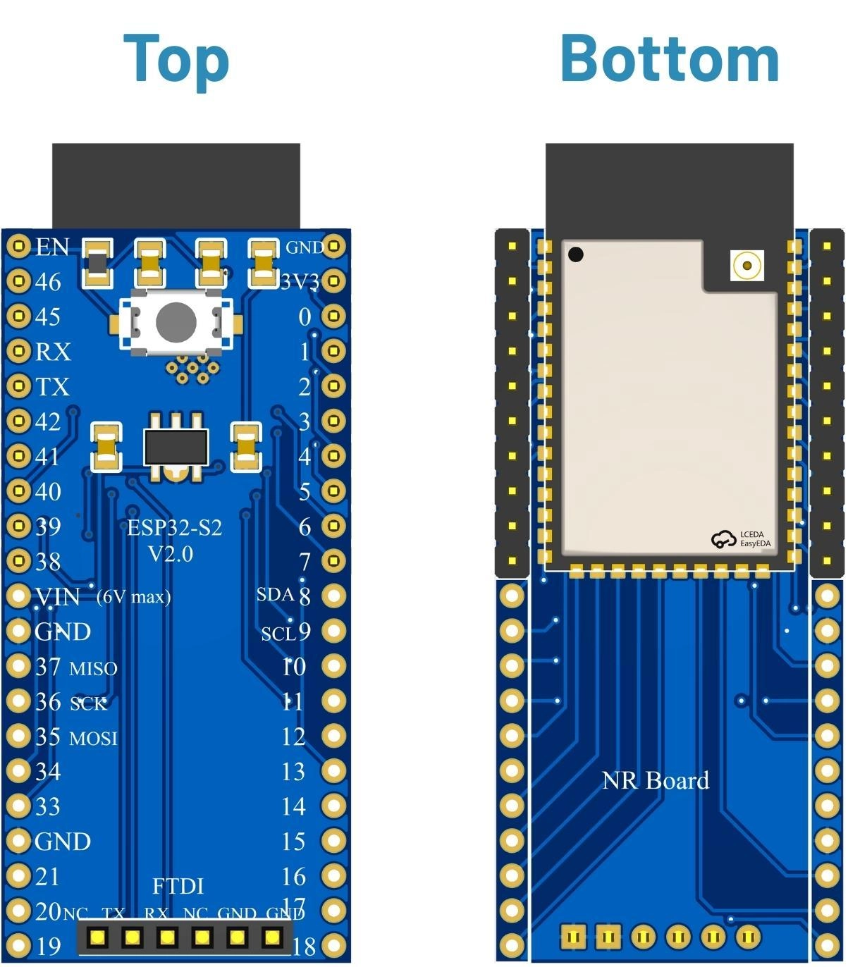
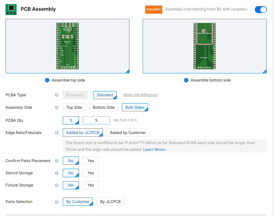
Figure: Component assembled view
Managing Assembly Yield and Inspection Risks
Inspecting Castellated ESP32 Modules with AOI
Visible Fillets: The primary advantage of the castellated module is that AOI (and human inspection) can easily verify the solder joints on the side. You want to see a shiny concave fillet rising up the side of the half-hole.
Understanding First-Pass Yield (FPY) Risks in Module Assembly
Yield is generally very high for modules. The main risk is "Head-in-Pillow", where the paste melts but doesn't wet to the module pin because the board warped or the pin was slightly oxidized.
| Risk Factor | Impact |
|---|---|
| Head-in-Pillow | Open circuit |
| Solder Balls | Shorts under shield |
| Antenna Shielding | Poor Range |
Bring-Up and Validation of the ESP32 Module PCBA
1. Impedance Check: Measure resistance between VCC and GND. Expect >1kΩ.
2. UART via FTDI: Connect your FTDI adapter. Hold BOOT, press EN.
Success: The Serial Terminal (115200 baud) shows waiting for download. This confirms the module is soldered correctly, powered, and the UART0 pins are connected.
3. RF Performance: Run a Wi-Fi scan sketch. If RSSI is weak, check if you accidentally placed a ground plane under the antenna area.
Further read: Discover the Power of ESP32 Microcontroller Projects
Conclusion
Utilizing the ESP32-S2 SMD-41P Module to custom PCB design brings a considerable reduction of the barrier of entry over a bare chip. Manufacturing of professional-quality IoT hardware with high reliability can be achieved by using JLCPCB's automated assembly through focusing on the mechanical integration - particularly antenna keep-outs and castellated pad soldering.
FAQs
Q1. Why are microcontroller boards more sensitive to PCBA quality than analog boards?
Microcontrollers are sensitive to power integrity, solder joint reliability, and transient current behavior. Assembly defects such as insufficient decoupling, cold joints, or misaligned packages can prevent boot or cause intermittent failures.
Q2. Can microcontroller modules be reliably assembled using SMT?
Certainly! There are joint features on the castellated pads if the stencil design (aperture size) and pick-and-place alignment rules are adequately followed.
Q3. What is the reason for the failure of microcontroller boards after assembly despite correct schematics?
Most of the time, the failures are caused by power integrity problems (wrong capacitor placement) or solder joint defects (tombstoning, cold joints) rather than by logic errors.
Q4. Does JLCPCB support ESP32 and other microcontroller chip module sourcing and assembly?
Yes, JLCPCB PCBA will use their affiliation with global partner to source different microcontroller chip modules as well as to simplify the supply chain for custom boards, thus, making the whole process of obtaining custom boards less complicated.
Popular Articles
• How to Create a Bluetooth-Controlled Car With Arduino: A Step-by-Step Guide
• How to Design and Assemble a Reliable ESP32 Module PCB on a 2-Layer Board
• The Ultimate Guide to Relay Symbol: Coil, Contacts, Diagrams, and Circuit Applications
• How to Identify SMD LED Polarity: Markings, Testing, and PCB Tips
• The Ultimate Guide to PCBA: Process,Types and Techniques for the Electronics Enthusiast
Keep Learning
How to Design an ESP32-S3 Development Board from Scratch: A 4-Layer PCB Design Tutorial
Designing your own ESP32-S3 development board gives you complete control over your hardware architecture while preparing your IoT projects for commercial production. Instead of relying on bulkier, off-the-shelf boards, building a custom design allows you to optimize the board space, expose only the required GPIO pins, and integrate peripherals directly onto a single substrate. In this tutorial, we will design a 4-layer ESP32-S3 development board from scratch. We will walk through the entire hardware d......
Arduino LED Driver Tutorial: Control More LEDs with 74HC595 and MAX7219
Arduino GPIO pins run out quickly in larger LED projects. By utilizing dedicated LED drivers and expansion ICs, you can drastically reduce pin usage, eliminate processor-heavy multiplexing loops, and simplify display wiring. In this guide, you will learn the operational architecture, wiring configurations, cascading techniques, and optimization strategies for the 74HC595 shift register and the MAX7219 LED driver. Why Arduino Projects Need LED Driver ICs Arduino GPIO and Current Limitations An ATmega32......
How to Create a Bluetooth-Controlled Car With Arduino: A Step-by-Step Guide
This tutorial walks through the complete engineering and implementation of a two-wheel Bluetooth RC car with an Arduino Nano module on a specially designed PCBA (Printed Circuit Board Assembly). While many hobbyists start by wiring motors and Bluetooth modules with jumper cables on a breadboard, this approach is prone to disconnection and signal noise. This guide upgrades that process by teaching you how to design a professional mainboard. Key Design Features Controller: Arduino Nano used as a plug-in......
Fiducial Marks in PCB and SMT Assembly: A Complete Guide to Accuracy and Design Rules
Modern Printed Circuit Boards (PCBs) are complex, integrating high-density components like 0.4mm pitch Ball Grid Arrays (BGAs), 0201 passives, and fine-pitch Quad Flat No-Lead (QFN) packages. In this advanced manufacturing environment, achieving placement accuracy measured in micrometers is crucial. A significant challenge in automated manufacturing is how pick-and-place machines, which handle thousands of components per hour, precisely locate the PCB. A board on a conveyor system is never in the perf......
Alternating Current vs Direct Current (AC vs DC): What's the Difference?
Electric current flows in two primary forms: alternating current (AC) and direct current (DC). AC periodically reverses direction, while DC flows steadily in one direction. AC powers the industrial and residential electrical grids, while DC powers batteries, electric vehicles, and nearly all modern consumer electronics. Understanding the core differences between AC and DC matters when designing power supplies, selecting electronic components, or laying out printed circuit boards (PCBs). This guide com......
Arduino LED Multiplexing Tutorial: Control More LEDs with Fewer Pins
The Arduino Uno is a powerful tool for prototyping, but driving multiple LEDs directly quickly exhausts its 20 GPIO pins and its 200 mA absolute maximum package current limit. To bypass these hardware bottlenecks, engineers and hobbyists use LED multiplexing to scale display outputs efficiently without upgrading the microcontroller. In this guide, you will learn the core principles of LED matrix scanning, Charlieplexing, refresh timing, ghosting fixes, and practical Arduino code without relying on any......