
How to Read a MOSFET Symbol: NMOS, PMOS, Arrows, and Body Diodes
14 min
- How to Read a MOSFET Symbol: 5 Visual Cues
- MOSFET Types and Symbols
- Understanding the MOSFET Symbol: What Each Line, Arrow, and Terminal Means
- MOSFET Terminal Labels: Gate, Source, Drain, and Body
- How to Read the Arrow on a MOSFET Symbol
- NMOS Symbol vs PMOS Symbol: Key Differences
- Enhancement vs Depletion Mode MOSFET Symbols
- 4-Terminal vs 3-Terminal MOSFET Symbols
- MOSFET Body Diode Symbol
- Simplified MOSFET Symbols in CMOS and IC Schematics
- MOSFET Symbol vs JFET Symbol: Key Visual Difference
- MOSFET Symbol Standards: IEEE, ANSI, and IEC Conventions
- MOSFET Symbols in EDA Tools: KiCad, LTspice, EasyEDA, and Altium
- FAQs About MOSFET Symbols
- Conclusion
If you have ever opened a schematic and stared at a MOSFET symbol wondering which terminal is the source, why the gate has a gap, or why the arrow points differently on two seemingly identical symbols — you are not alone.
The MOSFET schematic symbol packs four independent pieces of information into one small graphic: channel polarity, operating mode, terminal identity, and device type. Read those four cues correctly, and any MOSFET symbol becomes immediately clear, whether you encounter it in a power-electronics datasheet, a CMOS logic diagram, or an EDA library.
What this guide covers:
- How to identify NMOS and PMOS symbols
- How arrow direction change between IEEE/IEC and simplified IC symbols
- Enhancement-mode vs depletion-mode MOSFET symbols
- 3-terminal vs 4-terminal MOSFET symbols
- Body-diode orientation in power MOSFETs
- MOSFET symbol conventions used in datasheets, CMOS schematics, and EDA tools
How to Read a MOSFET Symbol: 5 Visual Cues

Figure: Schematic Breakdown of an N-Channel Enhancement MOSFET Symbol
| Feature | Meaning |
|---|---|
| Arrow In | NMOS (Detailed Style) |
| Arrow Out | PMOS (Detailed Style) |
| Dashed Channel | Enhancement Mode (Normally OFF) |
| Solid Channel | Depletion Mode (Normally ON) |
| Gate Bubble | PMOS (IC Style) |
These five visual cues are enough to identify most NMOS, PMOS, enhancement-mode, and depletion-mode MOSFET symbols found in datasheets and circuit schematics.
MOSFET Types and Symbols
Two channel polarities multiplied by two operating modes yield the four canonical MOSFET symbols.
| Type | Arrow Direction (IEEE/IEC) | Channel Line | Default State | VGS Required to Turn ON |
|---|---|---|---|---|
| N-channel Enhancement | Inward | Dashed | OFF | Positive (VGS > +Vth) |
| P-channel Enhancement | Outward | Dashed | OFF | Negative (VGS < -Vth) |
| N-channel Depletion | Inward | Solid | ON | Negative (to turn OFF) |
| P-channel Depletion | Outward | Solid | ON | Positive (to turn OFF) |
- N-channel Enhancement (NMOS): Characterized by an inward arrow and a dashed channel line. This is the most common MOSFET type, utilized heavily for low-side switching in buck converters, H-bridges, and motor drivers.
- P-channel Enhancement (PMOS): Characterized by an outward arrow and a dashed channel line. Commonly used for high-side switching and reverse-polarity protection circuits.
- N-channel Depletion: Features an inward arrow and a solid channel line. It remains on at VGS = 0.
- P-channel Depletion: Features an outward arrow and a solid channel line. This is the rarest commercial type.
Understanding the MOSFET Symbol: What Each Line, Arrow, and Terminal Means
A standard MOSFET symbol is built from three structural elements. Understanding these elements is fundamental when comparing BJTs versus MOSFETs, as MOSFETs operate purely on electrostatic fields rather than minority carrier injection.
The Channel Line: Solid vs Dashed
The vertical line at the centre represents the semiconductor channel — the physical current path between the drain and the source. Its style is not decorative:
- A broken or dashed line (three short segments) means no channel exists at VGS = 0, identifying an enhancement-mode device.
- A solid continuous line means a channel exists by default at VGS = 0, identifying a depletion-mode device.
The Gate Structure and the Insulating Gap
The gate is represented by a horizontal line that approaches the channel but does not touch it. This physical gap represents the insulating silicon dioxide (SiO2) layer. This insulating barrier is the defining visual and physical feature that separates a MOSFET symbol from a JFET symbol. In a JFET, the gate line touches the channel directly; in a MOSFET, it never does.
The Body Arrow: Meaning and Conventions
The arrow connects to the body (or substrate) terminal.
- In detailed four-terminal symbols, it points from the P-type to the N-type material, following standard PN junction diode conventions.
- In simplified three-terminal integrated circuit (IC) symbols, the arrow moves to the source leg and instead indicates the direction of conventional current flow.
Both conventions are in active use across modern electronics schematics.
MOSFET Terminal Labels: Gate, Source, Drain, and Body
| Terminal | Label | Function | Representation in the Symbol |
|---|---|---|---|
| Gate | G | Voltage-controlled input, insulated from the channel by an oxide layer | Horizontal line with a visible gap from the vertical channel |
| Source | S | Origin of majority carriers; reference node for gate-source voltage (VGS) | End of the channel connected directly to the body arrow link (discrete) |
| Drain | D | Exit terminal for the majority of carriers; handles high voltage/current | Opposite end of the channel from the source terminal |
| Body | B | Substrate/Bulk forms the intrinsic PN junction body diode | Arrow pointing on the channel (detailed) or implicit/separate pin (IC) |
In virtually all discrete packages (such as TO-220, SOT-23, DPAK, or TO-247), the body is internally connected to the source pin during packaging. Consequently, the schematic symbols for these devices show only three external terminals.
However, in complex integrated circuit layouts where hundreds of transistors share a common substrate, the body appears as a separate, fourth physical connection.
Body Terminal Representation: Discrete vs IC Symbols
In a discrete-device symbol, a short internal line connects the arrow directly to the source pin. This makes the body-to-source short circuit explicit and helps engineers immediately identify the polarity of the intrinsic body diode.
In IC schematics, the body either appears as an independent fourth pin tied directly to VSS (for NMOS) or VDD (for PMOS), or it is omitted entirely, with a gate bubble marking PMOS polarity instead.
How to Read the Arrow on a MOSFET Symbol
The arrow is the most frequently misread element in the MOSFET symbol because two distinct design conventions use the same graphical element for different purposes.
Arrow Direction in IEEE/IEC Four-Terminal MOSFET Symbols
In detailed four-terminal symbols, the arrow sits on the body terminal connection (the bulk substrate) and always points from P-type to N-type semiconductor material. This mimics standard diode polarity:
- NMOS (N-channel): The body is P-type material, and the channel is N-type. Therefore, the arrow points inward (P to N). Mnemonic: "N is in."
- PMOS (P-channel): The body is N-type material, and the channel is P-type. Therefore, the arrow points outward (N to P).
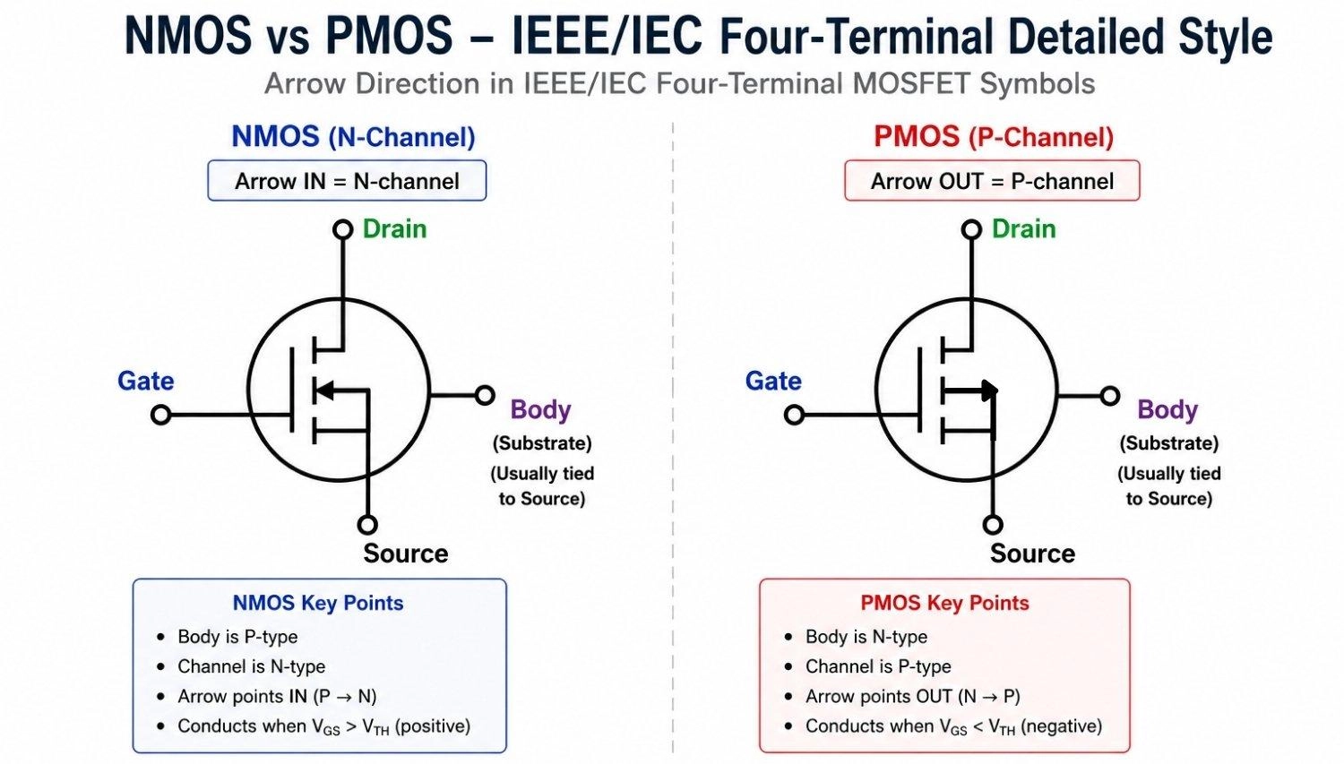
Figure: Comparison of NMOS and PMOS in IEEE/IEC Four-Terminal Detailed Style
Source-Leg Arrow in Simplified MOSFET Symbols
In simplified three-terminal symbols, the body is implicit. The arrow moves directly to the source leg, showing the direction of conventional current when the device is actively conducting:
- NMOS (simplified): The source-leg arrow points outward (away from the gate).
- PMOS (simplified): The source-leg arrow points inward (toward the gate).
This is the exact reverse of the detailed style. An NMOS has an inward arrow in detailed style but an outward arrow in simplified style. Both are correct; they simply follow different engineering standards.
Identifying the Arrow Convention: Detailed vs Simplified Style
To avoid errors, identify the overall schematic style first.
Ask yourself: Is the body drawn as a separate connection or directly tied to the source inside the symbol?
- If Yes: You are looking at the detailed IEEE/IEC style. The arrow shows the physical PN junction direction (inward = NMOS, outward = PMOS).
- If No: You are looking at the simplified IC style. The arrow shows conventional current direction on the source terminal (outward source = NMOS, inward source = PMOS).
Power-electronics datasheets almost always use the detailed style, while CMOS and digital-logic schematics almost always use the simplified style.
NMOS Symbol vs PMOS Symbol: Key Differences
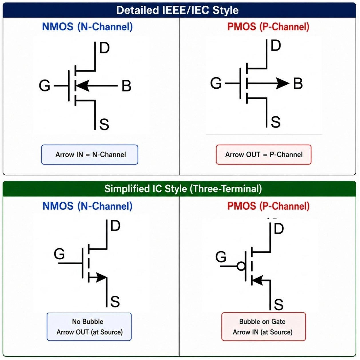
Figure: NMOS and PMOS MOSFET symbols compared in both detailed four-terminal IEEE/IEC style and simplified IC three-terminal style.
NMOS Symbol Features
- Arrow points inward (detailed style) or outward on the source leg (simplified style).
- No gate bubble is used in IC style.
- The body diode anode is at the source, and the cathode is at the drain.
- Turns on with positive VGS (VGS > Vth).
- Positioned typically as a low-side switch.
PMOS Symbol Features
- Arrow points outward (detailed style) or inward on the source leg (simplified style).
- A gate bubble is present in IC style.
- The body diode anode is at the drain, and the cathode is at the source.
- Turns on with negative VGS (VGS < -Vth).
- Positioned typically as a high-side switch.
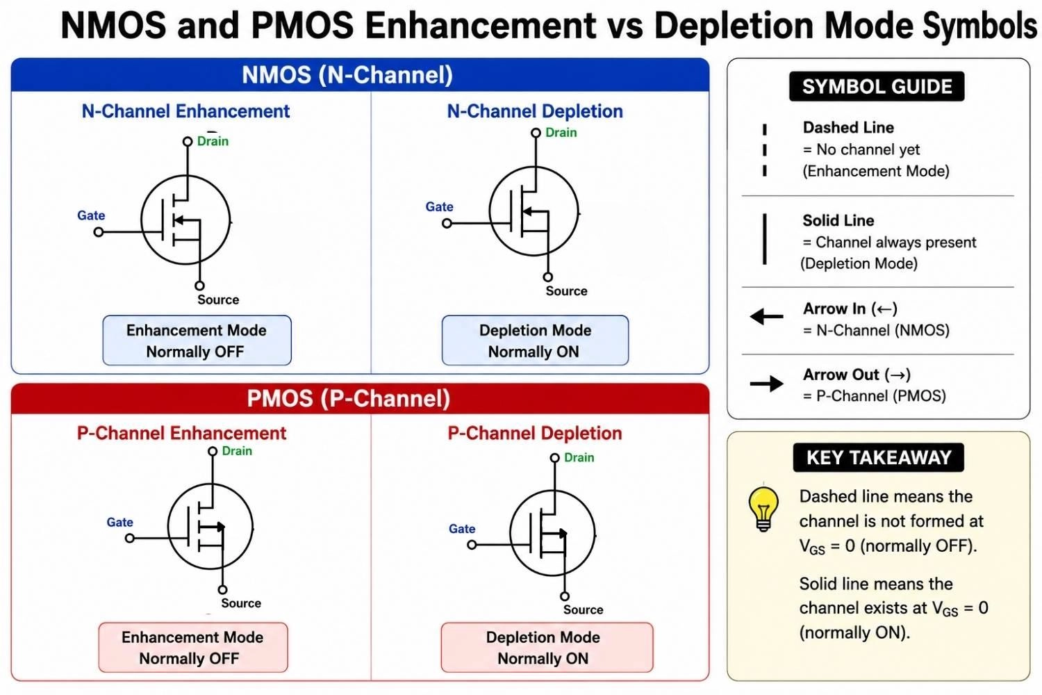
Enhancement vs Depletion Mode MOSFET Symbols
Understanding the distinction between enhancement and depletion modes is crucial when selecting surface-mount devices for your design.
Figure: Enhancement vs Depletion Mode Symbol Comparison
Broken or Dashed Channel Line: Enhancement-Mode MOSFET Symbol (Normally OFF)
A broken channel line, consisting of three short vertical segments, indicates that no conduction channel exists at VGS = 0. The device is naturally off. A channel forms only when the magnitude of the gate-to-source voltage (|VGS|) exceeds the threshold voltage (Vth). Enhancement-mode parts dominate the semiconductor market: virtually every discrete power MOSFET and all standard CMOS logic devices are enhancement-mode.
Solid Channel Line: Depletion-Mode MOSFET Symbol (Normally ON)
A solid, continuous channel line means a conduction channel exists at VGS = 0; the device is naturally on. An applied gate-to-source voltage of the opposite polarity is required to deplete the channel and pinch off current flow. Depletion-mode devices are specialized parts found mainly in constant-current sources, analog RF circuits, and self-biased startup topologies.
4-Terminal vs 3-Terminal MOSFET Symbols
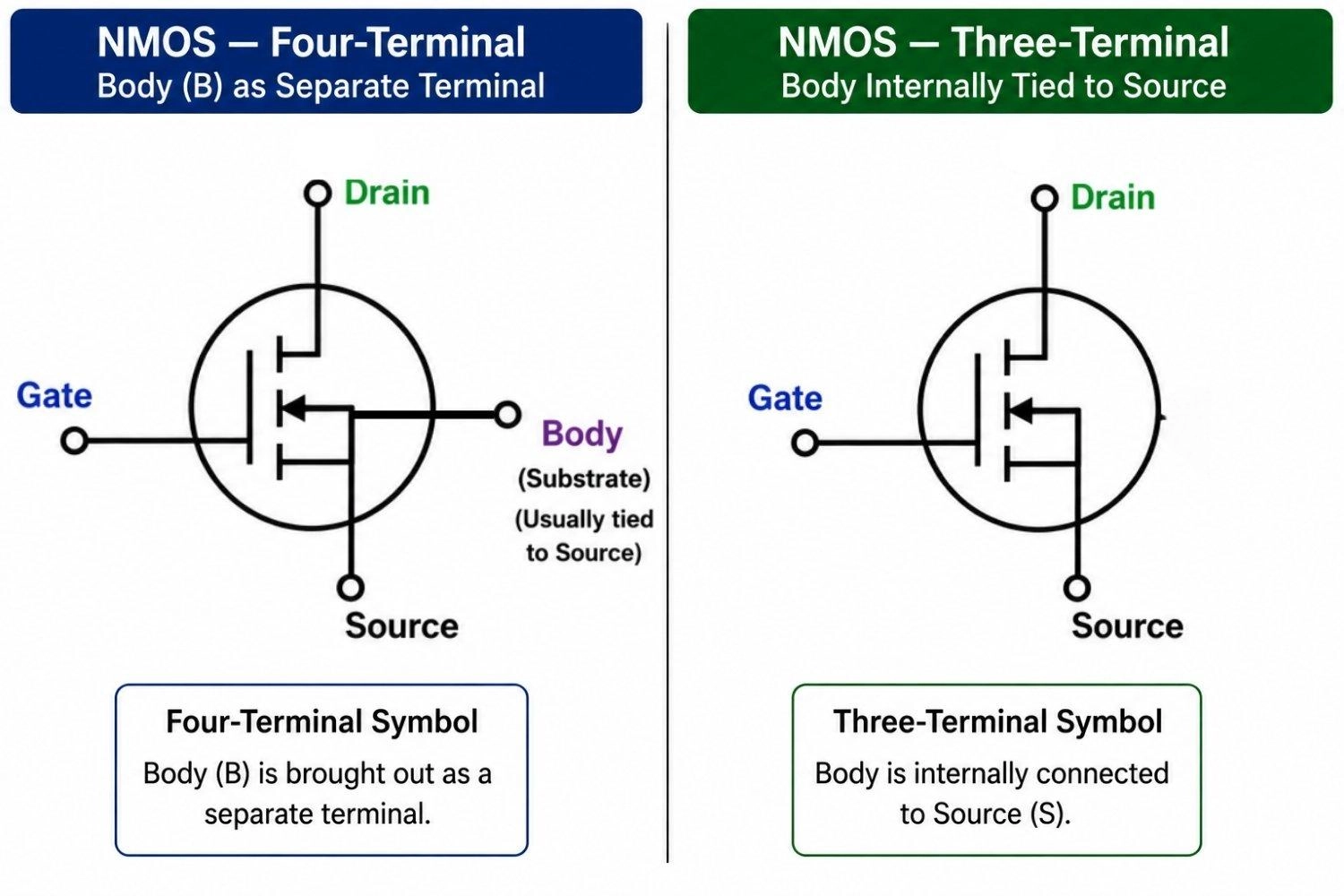
Figure: Comparison of 4-Terminal and 3-Terminal Symbols
In integrated circuits, transistors share a common silicon substrate. Therefore, the body terminal connects to a common substrate supply rail (VSS for NMOS, VDD for PMOS) rather than the individual source pin of each transistor. EDA tools represent this with nmos4 and pmos4 four-terminal symbols. In discrete packages, the body is wire-bonded directly to the source internally, creating a three-terminal device where the body diode is always visible in power schematics.
When transitioning from schematic design to layout, understanding your package types is crucial. Deciding whether you choose surface-mount vs through-hole packages affects both thermal performance and board space.
MOSFET Body Diode Symbol
What the Intrinsic Body Diode Is and Why It Appears in the Symbol
The body diode is not an intentionally integrated component; it is an intrinsic, parasitic PN junction formed between the P-type body substrate and the N-type drain region (for an NMOS). Modern power MOSFET manufacturers explicitly include this in their symbols to remind designers of this parallel conduction path.
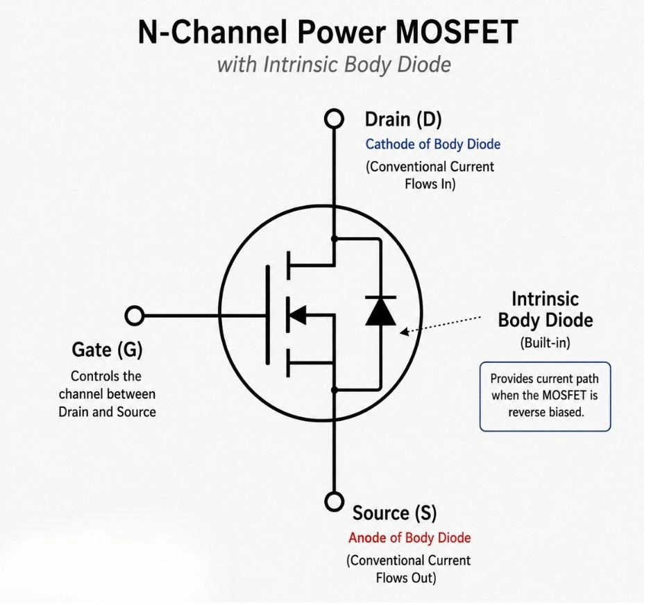
Figure: N-Channel Power MOSFET Symbol with Intrinsic Body Diode
Body Diode Orientation: NMOS vs PMOS
- NMOS Body Diode: The anode is at the source, and the cathode is at the drain. It conducts current whenever VDS goes negative, serving as a freewheeling path during dead time.
- PMOS Body Diode: The anode is at the drain, and the cathode is at the source. It conducts when VSD goes negative.
In high-frequency switching circuits, the body diode carries significant current during the switching transition dead times. Its reverse-recovery time (trr) and reverse-recovery charge (Qrr) are critical datasheet parameters, directly influencing switching losses and overall system efficiency.
Simplified MOSFET Symbols in CMOS and IC Schematics
The PMOS Gate Bubble — What It Means and What It Doesn't
A small circle (or bubble) on the gate of a simplified MOSFET symbol identifies a PMOS device. This bubble signals that the gate is active-low relative to the source.
Although it uses the same visual glyph as a logic-inversion bubble (such as on a NOT or NAND gate), it indicates P-type channel polarity rather than logical negation. Mistaking this gate bubble for a logic inverter is a common misreading in digital CMOS schematics.
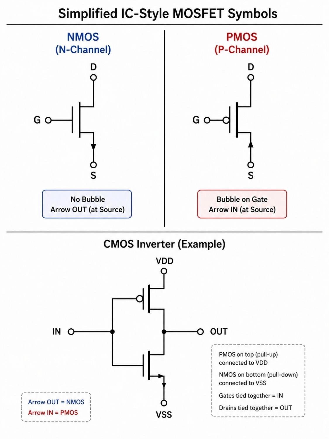
Figure: Simplified IC-style NMOS and PMOS MOSFET symbols with a CMOS inverter example showing how both symbols combine in practice.
Why Simplified MOSFET Symbols Omit Enhancement and Depletion Indicators
The simplified IC-style symbol completely omits the dashed/solid channel line distinction. When reading CMOS schematics, engineers assume enhancement mode unless explicitly stated otherwise, because depletion-mode devices are rarely used in standard digital CMOS processes.
MOSFET Symbol vs JFET Symbol: Key Visual Difference
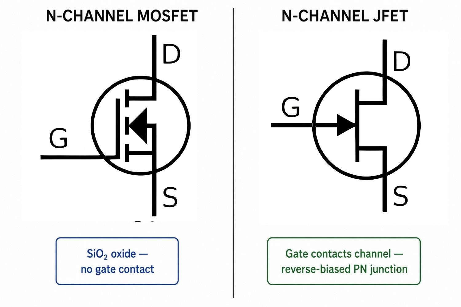
Figure: Schematic comparison of N-channel MOSFET symbol with oxide gap and N-channel JFET symbol with gate directly contacting the channel.
The primary visual difference between a MOSFET symbol and a JFET symbol is the physical gap between the gate line and the channel line.
- In the MOSFET symbol, the gate is insulated from the channel, and the physical gap represents the gate oxide layer.
- In the JFET symbol, the gate directly contacts the channel line, representing a physical, reverse-biased PN junction with no insulating layer.
An IGBT symbol, on the other hand, combines these elements: it features a MOSFET-style insulated gate but uses a BJT-style emitter arrow, with Collector (C) and Emitter (E) replacing the Drain and Source labels.
MOSFET Symbol Standards: IEEE, ANSI, and IEC Conventions
The dominant historical US standard was IEEE 315-1975 (also known as ANSI Y32.2-1975). Its supplement, IEEE 315A-1986, explicitly adopted IEC-derived MOSFET symbols. Both standards were officially inactivated by the IEEE on November 7, 2019.
The current active international standard is IEC 60617, maintained as an online database by the International Electrotechnical Commission. In practice, the MOSFET symbols in both modern standards are visually identical. The primary variation engineers encounter in modern schematics is not an IEEE-vs-IEC difference, but rather the split between detailed-discrete style and simplified-IC style.
MOSFET Symbols in EDA Tools: KiCad, LTspice, EasyEDA, and Altium
KiCad
KiCad provides a wide variety of NMOS, PMOS, enhancement-mode, depletion-mode, and four-terminal MOSFET symbols in its built-in Transistor_FET library. Both detailed IEEE/IEC styles and simplified digital styles are readily available.
LTspice
LTspice provides four default built-in MOSFET symbols:
- nmos and pmos (three-terminal)
- nmos4 and pmos4 (four-terminal with explicit body pins and editable channel width/length (W/L) parameters).
Use the four-terminal 4 variants for threshold-voltage sweeps and body-effect simulations. In SPICE netlists, all MOSFET instances are automatically prefixed with the character M (e.g., Mxxx Nd Ng Ns Nb <model>).
EasyEDA, Altium Designer, and Autodesk Eagle
EasyEDA, Altium Designer, and Eagle use simplified three-terminal MOSFET symbols in their default libraries.
Altium utilizes MOSFET_N and MOSFET_P with Altium 365 cloud portal integration, while Eagle's standard transistor.lbr provides generic NMOS and PMOS symbols.
Before sending your designs for manufacturing, double-checking the PCBA vs PCB differences helps avoid any layout-to-assembly mismatches.
FAQs About MOSFET Symbols
Q: Why does the source-leg arrow point outwards on some NMOS symbols but inwards on others?
It depends on the standard. In detailed 4-terminal symbols (IEEE/IEC), the substrate arrow points inward (P to N) for NMOS. In simplified 3-terminal symbols, the arrow moves to the source leg and shows conventional current flow (outward for NMOS).
Q: How can I identify the drain and source on a symmetrical MOSFET symbol?
On discrete symbols, the source is the terminal internally tied to the bulk substrate arrow. On symmetrical 4-terminal IC symbols, they are physically identical; the source is dynamically defined by the lower potential (NMOS) or higher potential (PMOS) during operation.
Q: Why do some power MOSFET symbols place the body diode outside the main transistor graphic?
It is a purely visual preference to improve schematic readability. The body diode is physically integrated into the silicon and cannot be removed, whether drawn internally or externally.
Q: Is the gate oxide gap in the MOSFET symbol always drawn to scale?
No, it is purely symbolic. While the real oxide layer is only nanometers thick, the gap is exaggerated on schematics to clearly distinguish the MOSFET from a JFET or BJT.
Q: Can a PMOS symbol have both a gate bubble and a source arrow?
Yes. Some CAD libraries combine both conventions (a gate bubble and an inward source arrow) to eliminate ambiguity regarding P-channel polarity.
Conclusion
Four visual cues decode any MOSFET symbol: the arrow direction identifies channel polarity (NMOS or PMOS), the channel line style identifies operating mode (enhancement or depletion), the body diode layout identifies the intrinsic source-drain diode, and the symbol style (detailed or simplified) tells you which arrow convention applies.

- You can source thousands of certified active components directly from the JLCPCB Parts Library.
- Simply upload your Gerber files to get an instant online quote and experience professional, high-quality, and fast PCB Assembly service with JLCPCB.
Popular Articles
• How to Identify SMD LED Polarity: Markings, Testing, and PCB Tips
• How to Create a Bluetooth-Controlled Car With Arduino: A Step-by-Step Guide
• How to Design and Assemble a Reliable ESP32 Module PCB on a 2-Layer Board
• The Ultimate Guide to Relay Symbol: Coil, Contacts, Diagrams, and Circuit Applications
• The Ultimate Guide to PCBA: Process,Types and Techniques for the Electronics Enthusiast
Keep Learning
How to Design an ESP32-S3 Development Board from Scratch: A 4-Layer PCB Design Tutorial
Designing your own ESP32-S3 development board gives you complete control over your hardware architecture while preparing your IoT projects for commercial production. Instead of relying on bulkier, off-the-shelf boards, building a custom design allows you to optimize the board space, expose only the required GPIO pins, and integrate peripherals directly onto a single substrate. In this tutorial, we will design a 4-layer ESP32-S3 development board from scratch. We will walk through the entire hardware d......
Circuit Breaker Symbols Explained: IEC, ANSI, MCB, and Pole Configuration Symbols
Electrical schematics are the universal language of power systems, control circuits, and printed circuit boards. Within these diagrams, the circuit breaker symbol is one of the most critical elements. Getting it right is essential for safety, troubleshooting, and manufacturing. An error as simple as mixing up a circuit breaker with a manual switch or an isolator can lead to catastrophic misinterpretations on the factory floor or during field maintenance. This guide provides a complete, technically acc......
How to Identify SMD LED Polarity: Markings, Testing, and PCB Tips
Surface-mount LED components are ubiquitous in electronics design, serving as everything from simple power indicators to complex lighting arrays. Unlike standard resistors, LEDs are polarized diodes. Identifying SMD LED polarity correctly is critical for prototype troubleshooting and high-volume PCB assembly. A reversed LED results in no light output, broken circuit paths, and potential diode breakdown if the reverse voltage exceeds the component's maximum rating (typically 5V or less for most indicat......
Arduino LED Driver Tutorial: Control More LEDs with 74HC595 and MAX7219
Arduino GPIO pins run out quickly in larger LED projects. By utilizing dedicated LED drivers and expansion ICs, you can drastically reduce pin usage, eliminate processor-heavy multiplexing loops, and simplify display wiring. In this guide, you will learn the operational architecture, wiring configurations, cascading techniques, and optimization strategies for the 74HC595 shift register and the MAX7219 LED driver. Why Arduino Projects Need LED Driver ICs Arduino GPIO and Current Limitations An ATmega32......
How to Create a Bluetooth-Controlled Car With Arduino: A Step-by-Step Guide
This tutorial walks through the complete engineering and implementation of a two-wheel Bluetooth RC car with an Arduino Nano module on a specially designed PCBA (Printed Circuit Board Assembly). While many hobbyists start by wiring motors and Bluetooth modules with jumper cables on a breadboard, this approach is prone to disconnection and signal noise. This guide upgrades that process by teaching you how to design a professional mainboard. Key Design Features Controller: Arduino Nano used as a plug-in......
Fiducial Marks in PCB and SMT Assembly: A Complete Guide to Accuracy and Design Rules
Modern Printed Circuit Boards (PCBs) are complex, integrating high-density components like 0.4mm pitch Ball Grid Arrays (BGAs), 0201 passives, and fine-pitch Quad Flat No-Lead (QFN) packages. In this advanced manufacturing environment, achieving placement accuracy measured in micrometers is crucial. A significant challenge in automated manufacturing is how pick-and-place machines, which handle thousands of components per hour, precisely locate the PCB. A board on a conveyor system is never in the perf......