
The Complete Guide to Transistor Symbol: Meaning, Types & Circuit Diagram Examples
15 min
- What Is a Transistor Symbol?
- Transistor Types and Symbols
- NPN vs PNP Transistor Symbol
- How to Read a Transistor Symbol
- Common Mistakes When Reading Transistor Symbols
- Transistor Symbol vs Other Circuit Symbol
- Transistor Symbol vs Physical Transistor
- Common Transistor Applications in Circuits
- Transistor Terminals Explained
- From Transistor Symbol to PCB: Design and Assembly Workflow
- FAQs about Transistor Symbol
- Conclusion
Whether you are a beginner stepping into electronics or an experienced engineer designing complex printed circuit boards, understanding how to read a transistor symbol is fundamental to interpreting schematic diagrams accurately. Transistors are used in everything from smartphones to power converters, acting as the fundamental building blocks of modern electronics. These symbols act as the bridge between theoretical circuit design and practical, real-world hardware. A single misread symbol can lead to incorrect footprint assignments, failing prototypes, or even damaged components.
To ensure your next project is a success, this transistor symbol explained guide will walk you through everything you need to know.
In this guide, you will learn how to:
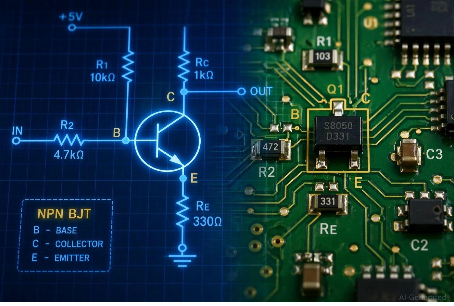
Figure: Electronic schematic blueprint transitioning to a physical printed circuit board with a highlighted transistor symbol.
What Is a Transistor Symbol?
In electronics, a transistor symbol is a standardized graphical representation used in schematic diagrams. Rather than depicting the component's physical appearance, every transistor schematic symbol conveys the device's electrical function and internal structure. The symbol immediately tells you how the component will behave when voltage or current is applied to its pins.
Purpose of Transistor Schematic Symbol in Circuit Diagrams
The primary purpose of a transistor symbol is universal communication. Circuit diagrams are the universal language of electronics. Standardized symbols ensure that a schematic designed in one part of the world can be perfectly understood, debugged, and manufactured anywhere else. They map out the logical connections before a single physical trace is laid down on a board.
Where Transistor Symbols are Used (Analog & Digital Circuits)
Every transistor symbol in a circuit diagram serves a specific purpose. In analog circuits, you will see them used for signal amplification (like in audio amplifiers or radio frequency transmitters). In digital circuits, they are primarily used as rapid switches, forming the fundamental logic gates, microprocessors, and memory modules.
Transistor Types and Symbols
When reviewing electronic transistor symbols, transistors are broadly classified into BJT, FET (including MOSFET and JFET), and advanced power devices like IGBT.
If you are diving deeper into electronics, you will need to understand this vast family. Depending on your project requirements-such as power handling, switching speed, or efficiency-you will have to choose the right BJT vs MOSFET symbol for your circuit.
| Transistor Family | Specific Type | Symbol Characteristics (Arrow & Lines) | Control Method | Common Application |
|---|---|---|---|---|
| BJT | NPN | Arrow on Emitter pointing OUT | Current-controlled | General switching, signal amplification |
| BJT | PNP | Arrow on Emitter pointing IN | Current-controlled | High-side switching, amplification |
| MOSFET | N-Channel (Enhancement) | Arrow pointing IN to substrate, broken channel line, insulated gate | Voltage-controlled | High-speed digital logic, power switching |
| MOSFET | P-Channel (Enhancement) | Arrow pointing OUT from substrate, broken channel line, insulated gate | Voltage-controlled | Load switching, power management |
| JFET | N-Channel / P-Channel | Arrow pointing IN (N) or OUT (P) at the gate terminal | Voltage-controlled | High input impedance audio amplifiers |
| IGBT | N/A | Insulated gate (like MOSFET) with Collector/Emitter (like BJT) | Voltage-controlled | High-voltage power electronics, motor drives |
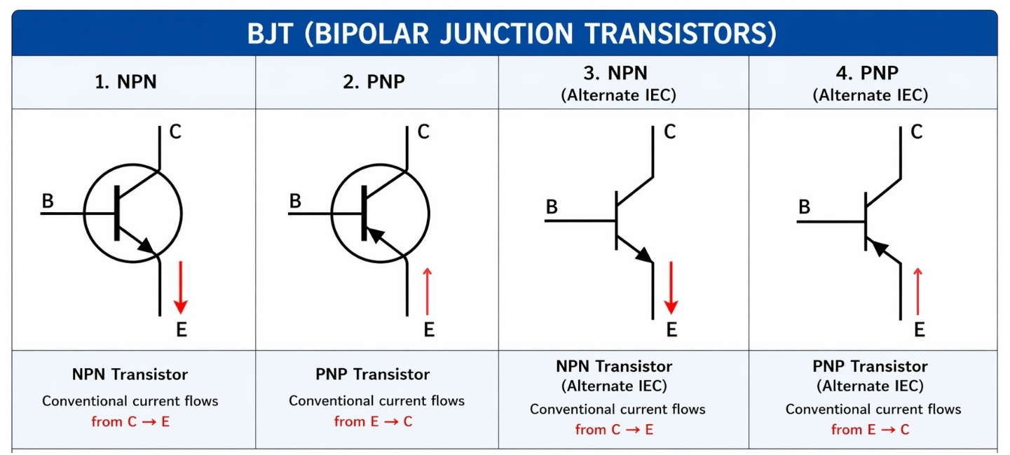
BJT Transistor Symbol (Bipolar Junction Transistor)
→ Current-controlled switches used for general amplification and logic.
- NPN → Standard current-controlled switch (arrow out).
- PNP → Standard current-controlled switch (arrow in).
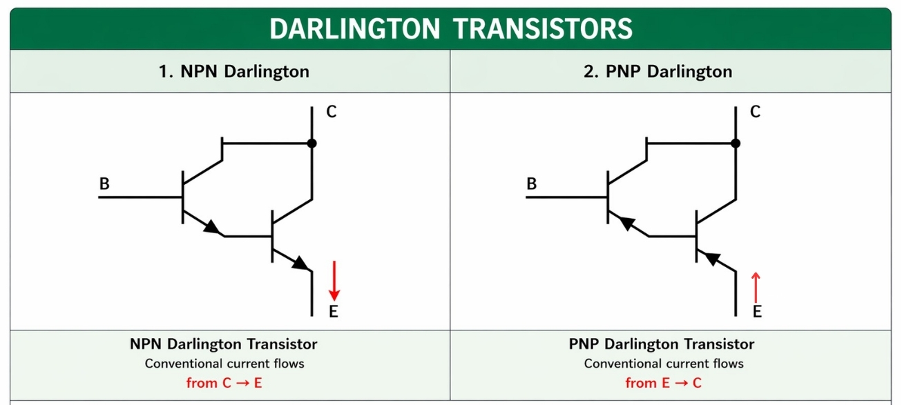
- Darlington Pair → Symbolized as two BJTs cascaded together in a single package. The emitter of the first connects to the base of the second, providing incredibly high current gain.
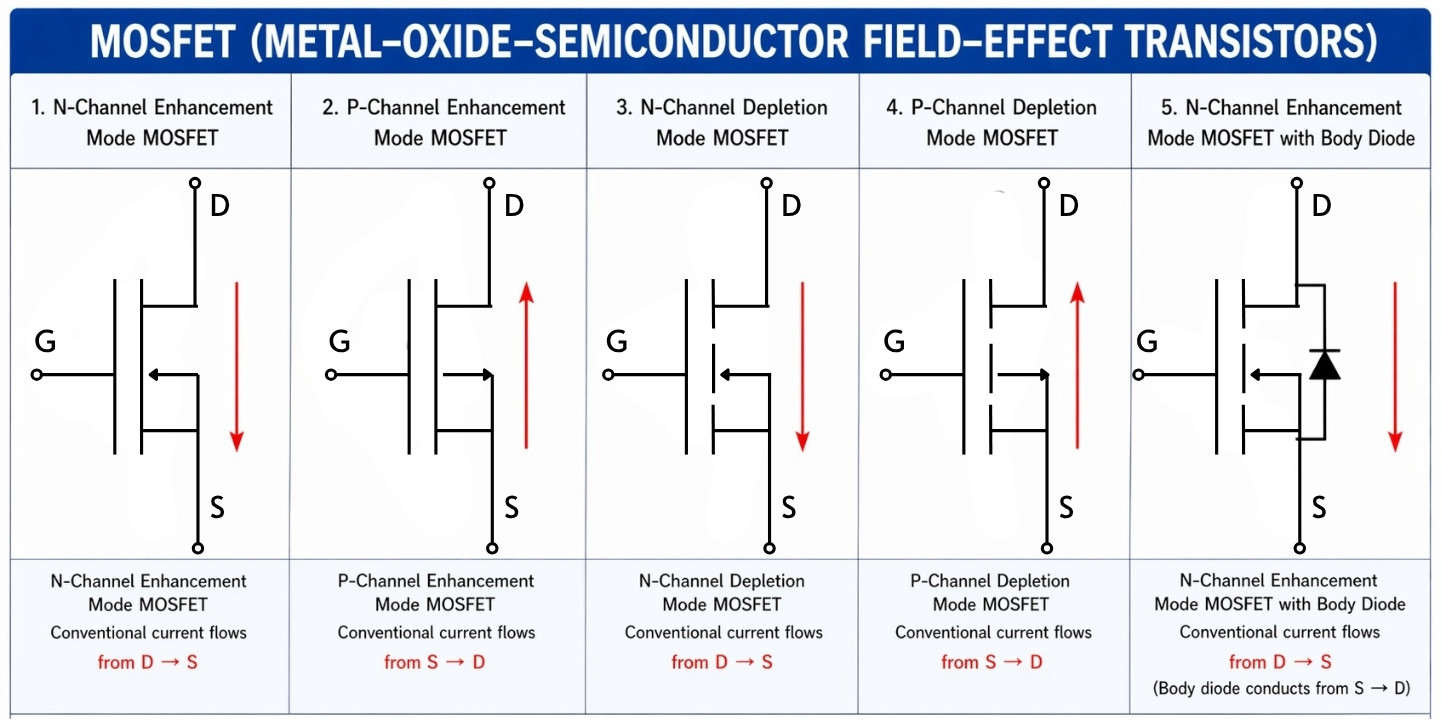
Field-Effect Transistor Symbol
→ Voltage-controlled devices used in high-efficiency and digital circuits.
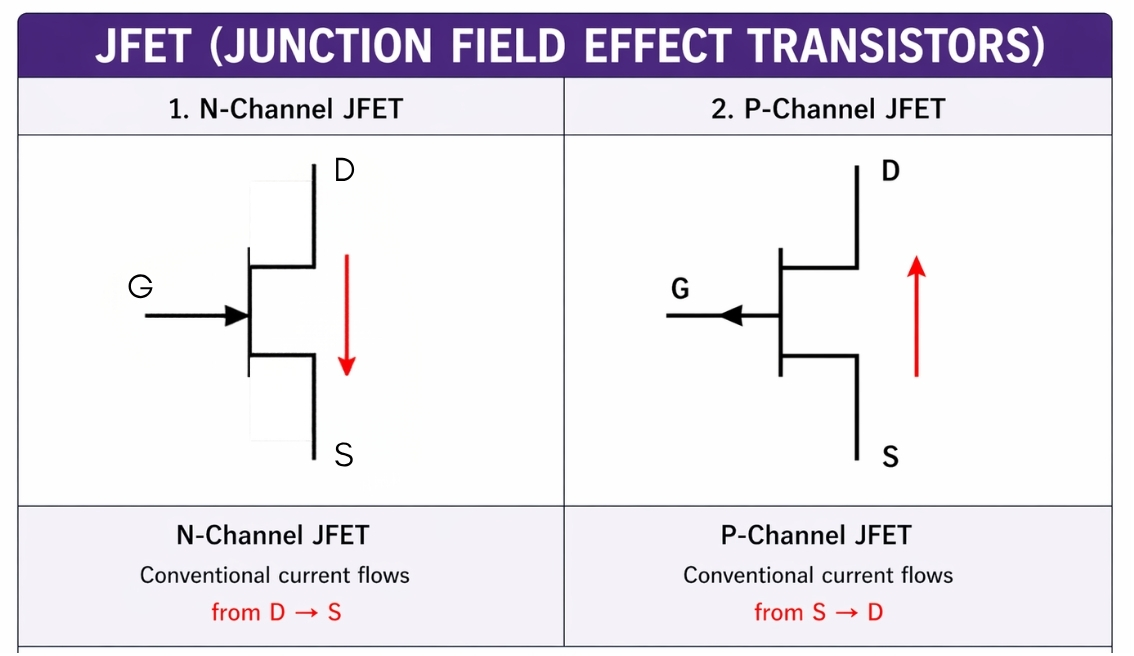
- JFET (Junction FET) → The simplest type of FET, functioning as a voltage-controlled resistor.
- MOSFET (Metal-Oxide-Semiconductor FET) → The most common transistor in modern digital electronics, featuring an insulated gate.
MOSFET Symbol Variations
In this MOSFET symbol explained breakdown, notice the specific differences indicating operating modes. Think of these modes like different types of "bridges" for electricity:
- Enhancement-mode (The "Broken Bridge") → Symbolized with a broken (dashed) line between the source and drain. This indicates the channel is normally "off." Just like a broken bridge, electricity cannot cross until you apply a gate voltage to "enhance" or build the bridge. It acts like a standard push-to-make switch.
- Depletion-mode (The "Solid Bridge") → Symbolized with a solid, continuous line. This indicates the device is normally "on." The bridge is already built, and current flows freely by default. You must apply a gate voltage to "deplete" or block the bridge to stop the current. Think of it like a push-to-break switch.
- N-channel vs P-channel → Just like NPN/PNP, the arrow direction on the central bulk/substrate line indicates the channel type. An inward arrow means N-channel; an outward arrow means P-channel.
JFET Symbol (Junction Field-Effect Transistor)
→ Voltage-controlled resistors for high input impedance.
- N-channel JFET → The arrow on the gate terminal points inward.
- P-channel JFET → The arrow on the gate terminal points outward.
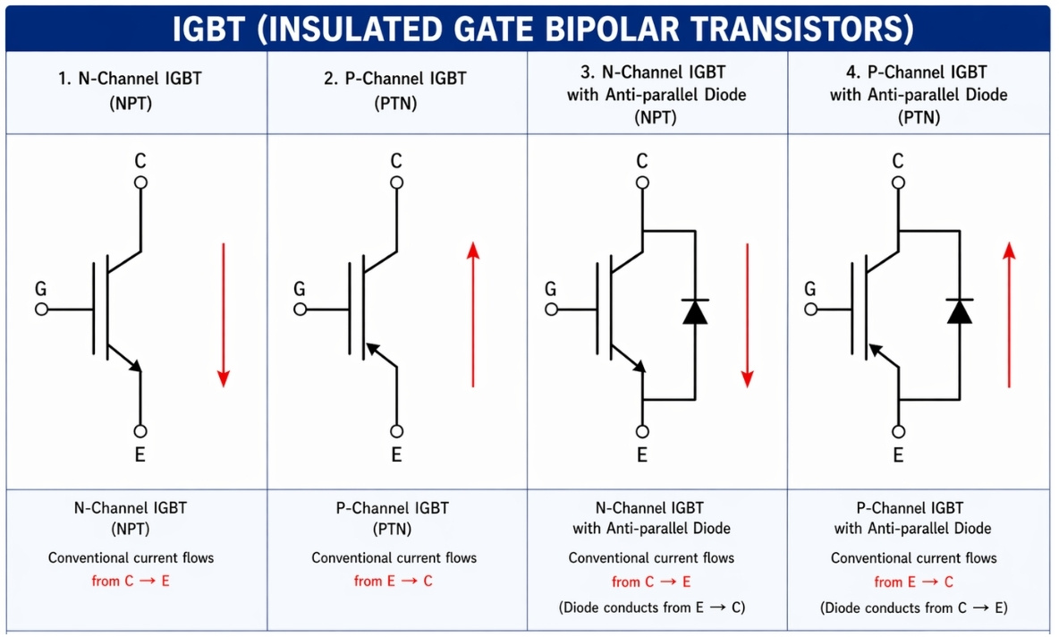
IGBT Symbol (Insulated Gate Bipolar Transistor)
→ Hybrid transistor for high-power applications.
The IGBT symbol looks like a hybrid. It features the isolated gate of a MOSFET but the collector/emitter terminals of a BJT. IGBTs are heavily used in power electronics, such as motor drives and electric vehicles, because they combine high efficiency and fast switching.
Special Transistor Types (Advanced)
- UJT Symbol (Unijunction Transistor) → Features one junction with two bases and an emitter. Used in oscillator circuits.
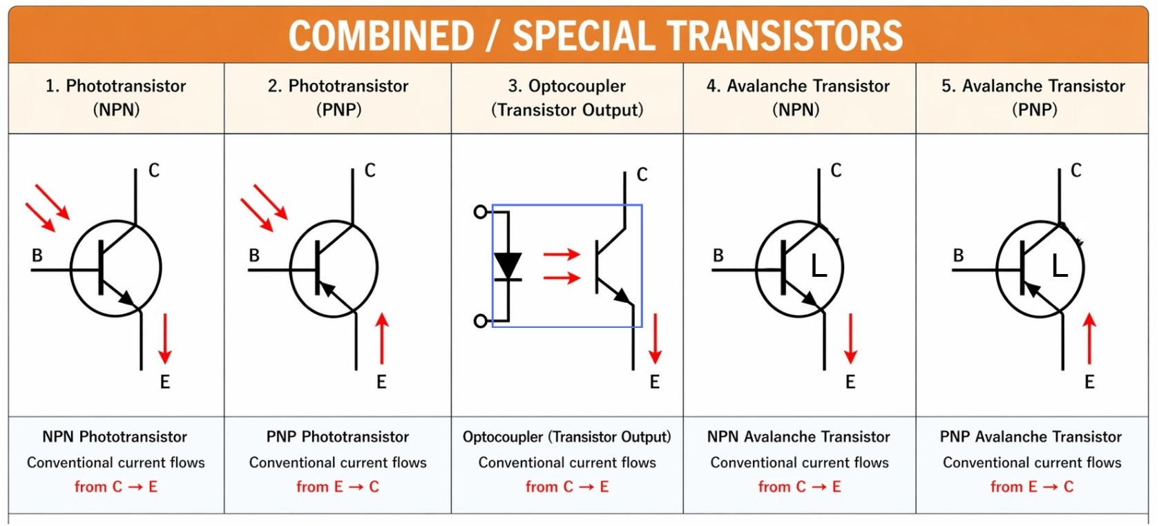
- Phototransistor Symbol → Symbolized with a standard BJT symbol but with two arrows pointing toward the base, representing incoming light that activates the device.
- RF Transistor → Designed specifically for high-frequency switching; symbols often include internal parasitic capacitors.
- Power Transistor Symbol → Functionally identical to standard BJTs/MOSFETs, but the schematic might annotate them with heat sink symbols or specific high-current ratings.
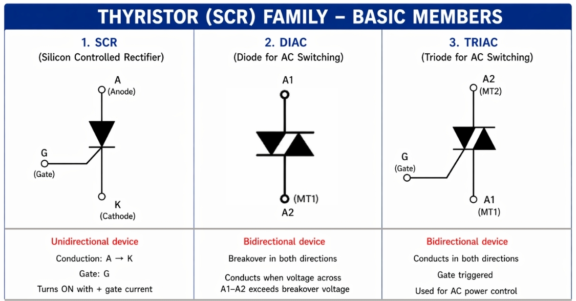
Thyristor Symbol (Important Extension)
While technically a different family, thyristors act as advanced electronic switches and are often grouped with transistors:
- SCR Symbol (Silicon Controlled Rectifier): → Symbolized like a diode with an extra "gate" terminal. It acts as a latching switch.
- TRIAC Symbol: → Symbolized as two inverse-parallel diodes with a gate, used to switch AC power.
- DIAC Symbol: → Looks like a bidirectional diode; used to trigger TRIACs.
NPN vs PNP Transistor Symbol
Because BJTs are so common, understanding the difference between the NPN transistor symbol diagram and the PNP is a frequent hurdle for beginners.
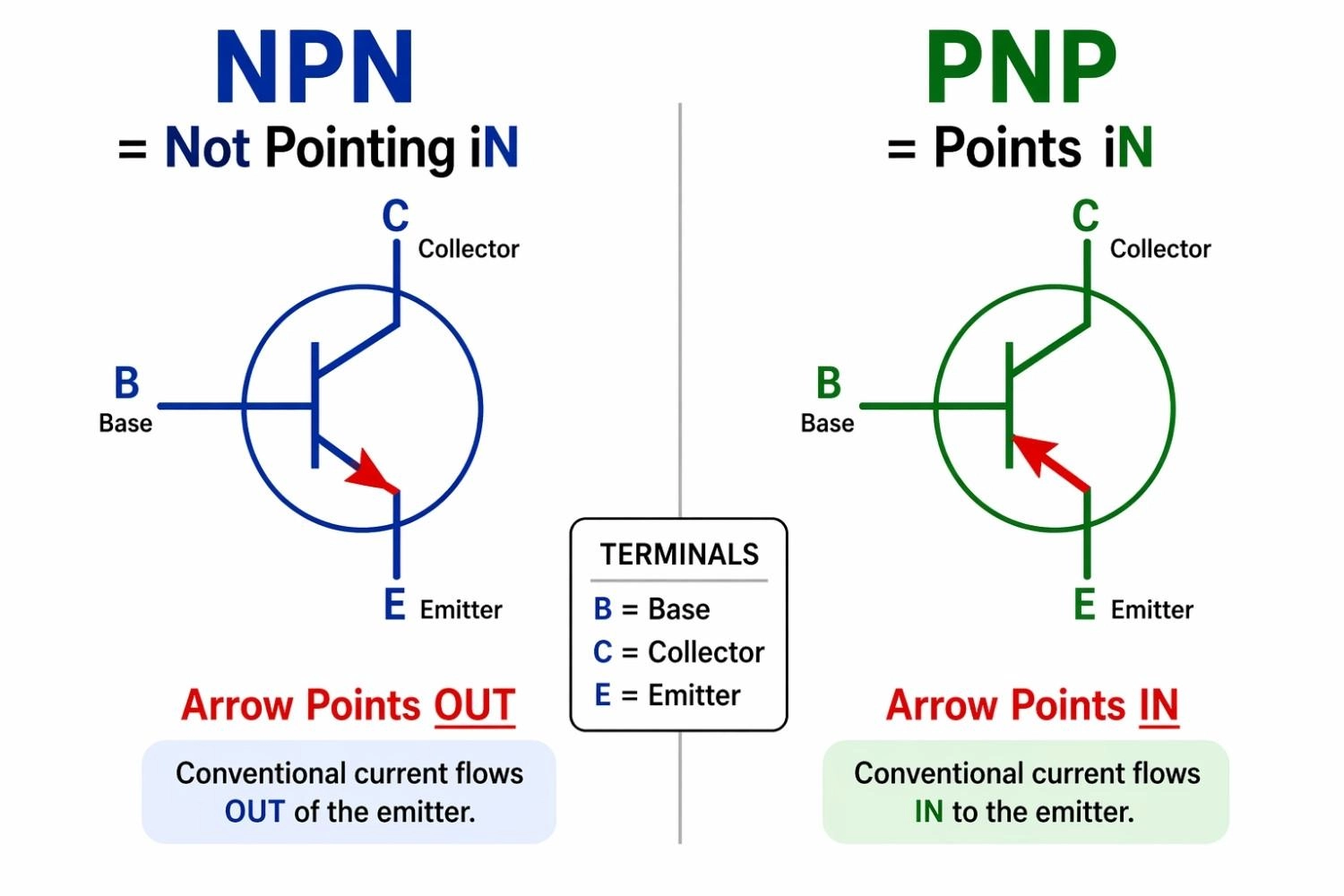
Figure: NPN vs PNP transistor symbol comparison emphasizing outward and inward emitter arrow directions with memory mnemonics.
NPN Transistor Symbol (Arrow Out)
In an NPN transistor, the arrow on the emitter points outward, away from the base. This indicates that current flows from the collector to the emitter when a positive voltage is applied to the base.
PNP Transistor Symbol (Arrow In)
In a PNP transistor, the arrow on the emitter points inward, toward the base. Here, current flows from the emitter to the collector, and the device is turned "on" by pulling the base to a lower voltage than the emitter.
NPN vs PNP Symbol: Key Differences
The physical difference lies in the arrangement of the semiconductor materials (N-type and P-type). Practically, they require opposite polarities to operate.
Mnemonic to Remember:
- NPN → Not Pointing iN (Arrow points out)
- PNP → Points iN (Arrow points in)
How to Read a Transistor Symbol
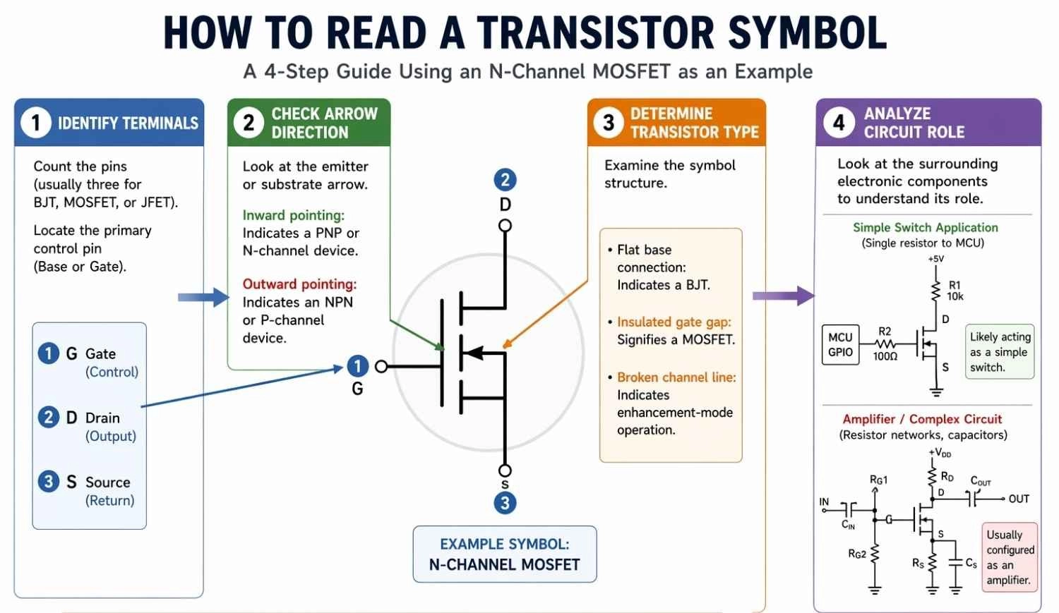
Figure: Step-by-step visual guide on how to read a transistor symbol in a circuit diagram.
Step 1: Identify Terminals
- Count the pins (usually three for BJT, MOSFET, or JFET).
- Locate the primary control pin (Base or Gate).
Step 2: Check Arrow Direction
- Look at the emitter or substrate arrow.
- Inward pointing: Indicates a PNP or N-channel device.
- Outward pointing: Indicates an NPN or P-channel device.
Step 3: Determine Transistor Type
- Flat base connection: Indicates a BJT.
- Insulated gate gap: Signifies a MOSFET.
- Broken channel line: Indicates enhancement-mode operation.
Step 4: Analyze Circuit Role
- Look at the surrounding electronic components.
- Single resistor to microcontroller: Likely acting as a simple switch.
- Complex resistor networks/capacitors: Usually configured as an amplifier.
Common Mistakes When Reading Transistor Symbols
Confusing NPN vs PNP: The most common error. Remember the mnemonic: NPN is Not Pointing iN.
Ignoring Arrow Direction: The arrow is not just decoration; wiring a PNP transistor like an NPN will result in a non-functional circuit and a potentially destroyed component.
Misidentifying Terminals: Swapping the Collector and Emitter in a BJT, or Drain and Source in a MOSFET, will lead to unexpected behavior. Always double-check device datasheets.
Transistor Symbol vs Other Circuit Symbol
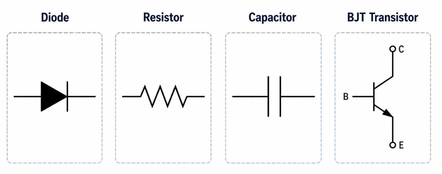
Figure: Comparison of electronic schematic symbols: Diode, Resistor, Capacitor, and Transistor.
Transistor vs Diode
- Diode Symbol: A simple triangle pressing against a line, acting as a one-way valve for current.
- Transistor Symbol: More complex, featuring a base/gate line and three distinct terminals.
- Key Difference: While a BJT internally contains two P-N junctions (like two diodes), its symbol explicitly shows the three terminals required for amplification or switching.
Transistor vs Resistor
- Resistor Symbol: Represented as a jagged line (US) or a simple rectangle (International).
- Function: Passively limits current flow, unlike the active control of a transistor
Transistor vs Capacitor
- Capacitor Symbol: Consists of two parallel lines separated by a gap (representing the dielectric).
- Key Difference: While MOSFETs also have a gap at the gate (representing gate capacitance), the overall symbol with drain and source terminals is distinctly different
Transistor Symbol vs Physical Transistor
One critical concept is that a schematic symbol does not represent the physical form of the transistor - it only defines the electrical behavior in a circuit.
Transistor Symbol Represents Electrical Function
- Defines transistor type (e.g., NPN, PNP, MOSFET).
- Shows terminal roles (B, C, E / G, D, S).
- Indicates current direction and circuit behavior.
- Focus: How the transistor works.
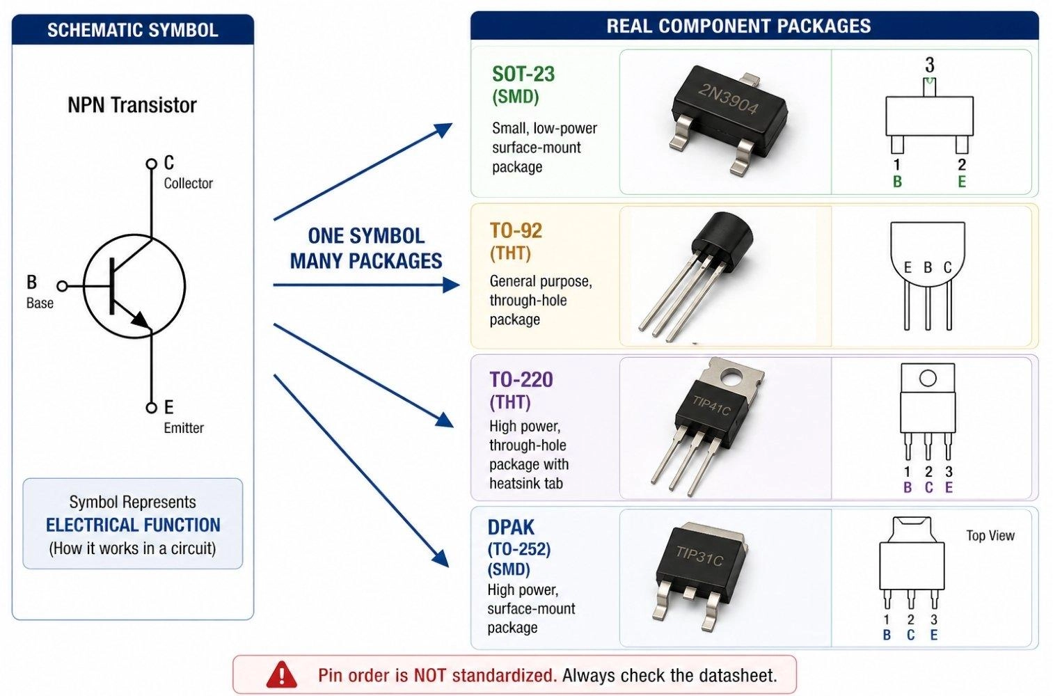
Figure: One NPN Transistor Symbol mapping to multiple physical packages, categorized into Through-Hole (TO-92, TO-220) and Surface-Mount (SOT-23, DPAK) types.
Package Represents Physical Implementations
- Defines mechanical form and mounting style.
- Common transistor packages:
- Through-Hole (THT) Types:
- TO-92: A small, semi-cylindrical plastic package with three straight wire leads, highly popular for low-power breadboarding and DIY prototypes.
- TO-220: A larger rectangular package featuring a prominent metal mounting tab for a heatsink, capable of handling high current.
- Surface-Mount (SMD/SMT) Types:
- SOT-23: A very small, rectangular plastic surface-mount package with three tiny flat gull-wing leads, ideal for dense PCB layouts and low-power signal switching.
- DPAK (TO-252) / SOT-223: Larger SMD packages designed to handle higher power and heat dissipation while maintaining a low-profile surface-mount footprint.
- Through-Hole (THT) Types:
- Determines: Thermal performance, current handling, and PCB footprint.
- Includes part markings or SMD codes used for physical identification.
- Focus: How the transistor is built and used.
Key Insight
One schematic symbol can map to multiple physical packages with different sizes, pin layouts, and power capabilities.
Same NPN symbol → can represent:
- Breadboard-friendly TO-92
- Compact SOT-23 for dense PCBs
- High-power TO-220 with heatsink
Warning
Pin order is not standardized across packages. For example, a TO-92 package may use E-B-C or C-B-E depending on the manufacturer.
Selection depends on electrical requirements (current/voltage), thermal limits, and PCB space-not the symbol.
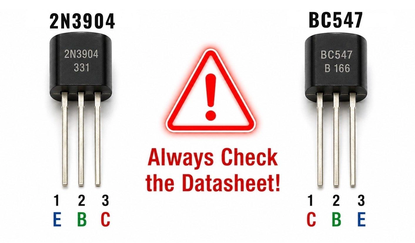
Figure: The TO-92 pinout trap showing different pin configurations (EBC vs CBE) for different transistor part numbers.
Common Transistor Applications in Circuits
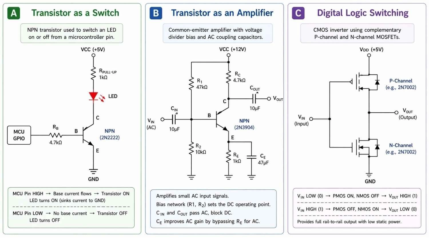
Figure: Circuit diagram examples showing an NPN transistor acting as a switch for an LED, configured as an analog signal amplifier, and a CMOS digital logic switching circuit.
Transistor as a Switch
- Operation Mode: Driven to saturation (fully on) or cutoff (fully off).
- Schematic Layout: Typically shows a base resistor to limit current.
- Load Placement: The load (like an LED or motor) is connected to the collector.
Transistor Amplifier
- Operation Mode: Operates in its active region to scale signals.
- Schematic Layout: Features biasing resistors connected to the base.
- Signal Routing: Uses coupling capacitors on the input and output to block DC voltages while allowing the AC signal to pass.
Digital Logic Switching
- Component Pairing: Features pairs of N-channel and P-channel MOSFETs (CMOS logic) drawn together.
- Switching Action: Toggling the gate voltage turns one transistor on while the other turns off.
- Output State: Pulls the final output distinctly high or low.
Transistor Terminals Explained
To read a schematic properly, you must identify the terminals represented on the symbol. Always verify terminal orientation using the component datasheet before PCB design to prevent catastrophic routing errors.
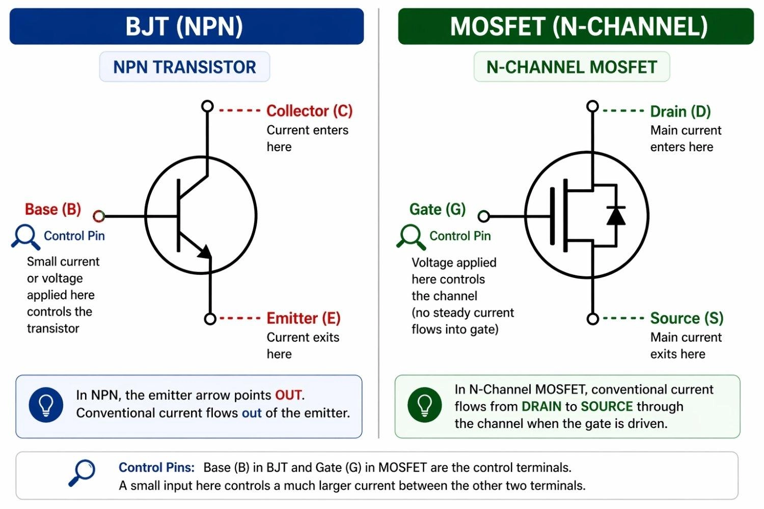
Figure: Transistor Terminals Explained: Base, Collector, Emitter and Gate, Drain, Source
Base, Collector, Emitter (BJT)
For Bipolar Junction Transistors (BJTs), the symbol features three main connection points:
- Base (B): The control pin. A small current here controls a larger current flowing through the device.
- Collector (C): The larger current enters here (in NPN type).
- Emitter (E): The current exits through this terminal. It is always the terminal that has the arrow.
Gate, Drain, Source (FET)
Field-Effect Transistors (FETs) use voltage rather than current for control, and their terminals are named differently:
- Gate (G): The control terminal, isolated from the main current path.
- Drain (D): The terminal where the main current enters the channel.
- Source (S): The terminal where the main current exits.
Arrow Direction Meaning (Current Flow)
The most critical feature for identification is the arrow. The transistor symbol arrow meaning directly dictates the direction of conventional current flow (from positive to negative). In BJTs, the arrow is always located on the Emitter. If the arrow points out, conventional current flows out of the emitter; if it points in, current flows into the emitter.
From Transistor Symbol to PCB: Design and Assembly Workflow
Transitioning your design from a digital schematic to a physical board requires accuracy and the right manufacturing partner. Incorrect transistor pin mapping is one of the most common causes of PCB failure during the first prototypes.
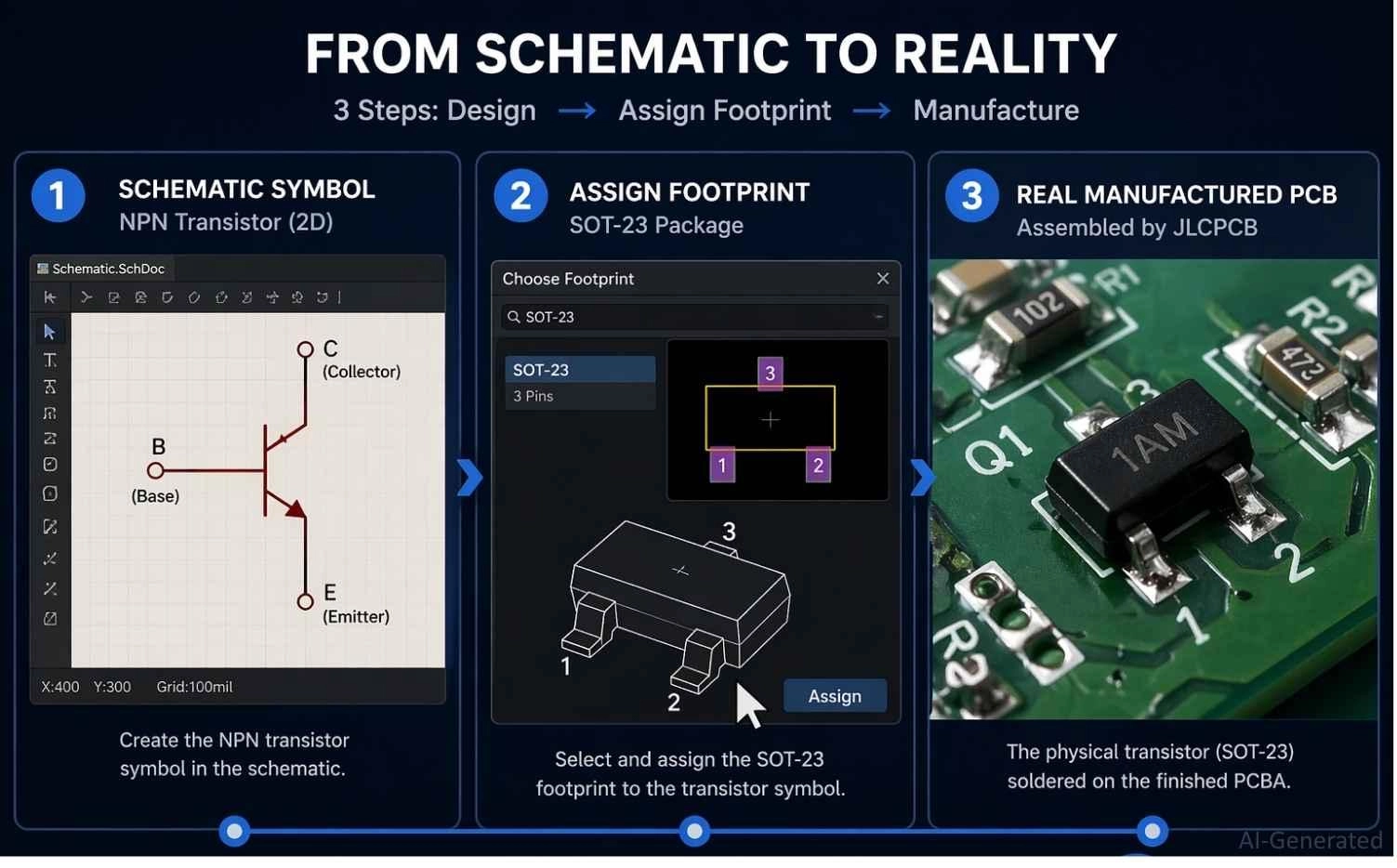
Figure: Workflow diagram showing the transition from a digital transistor schematic symbol to footprint assignment to a final manufactured PCBA by JLCPCB.
Transistor Schematic Symbol to PCB Workflow
Once the schematic is finalized, the EDA tool converts each transistor symbol into a physical footprint through the netlist and library mapping system.
The symbol defines logical pins (B, C, E / G, D, S)
The footprint defines physical pad locations and orientation
Key Technical Checks:
1. Ensure pin numbering matches datasheet (not just labels)
2. Verify correct mapping:
- BJT → Base, Collector, Emitter
- MOSFET → Gate, Drain, Source
3. Run ERC + netlist cross-probing to catch mismatches
Even a single swapped pin (e.g., C ↔ E) will make the circuit non-functional.
Transistor Schematic Symbol Footprint Assignment
A single transistor symbol can correspond to multiple package variants, so footprint selection must be datasheet-driven.
Common Packages:
- SOT-23 (SMD, compact)
- SOT-223 / DPAK (power SMD)
- TO-92 (through-hole, small signal)
- TO-220 (through-hole, power devices)
Critical Parameters:
- Pin order (e.g., E-B-C vs C-B-E varies by manufacturer)
- Pad pitch and spacing
- Thermal requirements (especially for power transistors)
Advanced Considerations:
- Add thermal pads or copper pours for high-current devices
- Ensure correct silkscreen orientation (Pin 1 / flat edge)
- Check package code marking (SMD transistor code) against datasheet
Never assume pinout consistency-even identical part numbers from different vendors may differ.
From Transistor Symbol to PCB Assembly with JLCPCB
PCB assembly services like JLCPCB streamline the transition from transistor schematic symbols to fully assembled PCBs, ensuring accurate component placement and efficient production.
If you are using surface-mount technology, understanding the SMD transistor code is vital for footprint matching.
To ensure you have access to the exact components you need, you can browse an extensive library of verified components on the JLCPCB Parts page.

- Upload Gerber files for PCB fabrication.
- Assign correct footprints using verified parts from the JLCPCB Parts library.
- Use PCB Assembly service for reliable production.
Accelerate your electronics journey with JLCPCB today!
FAQs about Transistor Symbol
Q: What does the arrow in a transistor symbol mean?
The arrow indicates the direction of conventional current flow through the device's emitter (BJTs) or source/substrate (FETs).
Q: How to identify NPN vs PNP quickly?
Look at the emitter arrow: OUT means NPN (Not Pointing iN), and IN means PNP (Points iN).
Q: What are transistor terminals?
Bipolar Junction Transistors (BJT) use Base, Collector, and Emitter terminals, while Field-Effect Transistors (FET) use Gate, Drain, and Source terminals.
Q: What is the MOSFET symbol difference?
MOSFET symbols feature an insulated gap at the gate, with lines indicating enhancement (broken) or depletion (solid) operating modes.
Q: Are SCR and TRIAC transistors?
No, they belong to the thyristor family, acting as latching semiconductor switches specifically designed for high-power AC applications.
Conclusion
Understanding transistor symbols is the foundational step toward mastering electronic circuit design. From distinguishing between an NPN's outward arrow and a PNP's inward arrow, to recognizing the complex insulated gate of a MOSFET, these symbols communicate everything you need to know about how current flows through your circuit.
By mastering these symbols and avoiding common pin-mapping mistakes, you can confidently turn any schematic diagram into a fully functional, reliable hardware project.
Popular Articles
• How to Identify SMD LED Polarity: Markings, Testing, and PCB Tips
• How to Create a Bluetooth-Controlled Car With Arduino: A Step-by-Step Guide
• How to Design and Assemble a Reliable ESP32 Module PCB on a 2-Layer Board
• The Ultimate Guide to Relay Symbol: Coil, Contacts, Diagrams, and Circuit Applications
• The Ultimate Guide to PCBA: Process,Types and Techniques for the Electronics Enthusiast
Keep Learning
How to Design an ESP32-S3 Development Board from Scratch: A 4-Layer PCB Design Tutorial
Designing your own ESP32-S3 development board gives you complete control over your hardware architecture while preparing your IoT projects for commercial production. Instead of relying on bulkier, off-the-shelf boards, building a custom design allows you to optimize the board space, expose only the required GPIO pins, and integrate peripherals directly onto a single substrate. In this tutorial, we will design a 4-layer ESP32-S3 development board from scratch. We will walk through the entire hardware d......
Circuit Breaker Symbols Explained: IEC, ANSI, MCB, and Pole Configuration Symbols
Electrical schematics are the universal language of power systems, control circuits, and printed circuit boards. Within these diagrams, the circuit breaker symbol is one of the most critical elements. Getting it right is essential for safety, troubleshooting, and manufacturing. An error as simple as mixing up a circuit breaker with a manual switch or an isolator can lead to catastrophic misinterpretations on the factory floor or during field maintenance. This guide provides a complete, technically acc......
How to Identify SMD LED Polarity: Markings, Testing, and PCB Tips
Surface-mount LED components are ubiquitous in electronics design, serving as everything from simple power indicators to complex lighting arrays. Unlike standard resistors, LEDs are polarized diodes. Identifying SMD LED polarity correctly is critical for prototype troubleshooting and high-volume PCB assembly. A reversed LED results in no light output, broken circuit paths, and potential diode breakdown if the reverse voltage exceeds the component's maximum rating (typically 5V or less for most indicat......
Arduino LED Driver Tutorial: Control More LEDs with 74HC595 and MAX7219
Arduino GPIO pins run out quickly in larger LED projects. By utilizing dedicated LED drivers and expansion ICs, you can drastically reduce pin usage, eliminate processor-heavy multiplexing loops, and simplify display wiring. In this guide, you will learn the operational architecture, wiring configurations, cascading techniques, and optimization strategies for the 74HC595 shift register and the MAX7219 LED driver. Why Arduino Projects Need LED Driver ICs Arduino GPIO and Current Limitations An ATmega32......
How to Create a Bluetooth-Controlled Car With Arduino: A Step-by-Step Guide
This tutorial walks through the complete engineering and implementation of a two-wheel Bluetooth RC car with an Arduino Nano module on a specially designed PCBA (Printed Circuit Board Assembly). While many hobbyists start by wiring motors and Bluetooth modules with jumper cables on a breadboard, this approach is prone to disconnection and signal noise. This guide upgrades that process by teaching you how to design a professional mainboard. Key Design Features Controller: Arduino Nano used as a plug-in......
Fiducial Marks in PCB and SMT Assembly: A Complete Guide to Accuracy and Design Rules
Modern Printed Circuit Boards (PCBs) are complex, integrating high-density components like 0.4mm pitch Ball Grid Arrays (BGAs), 0201 passives, and fine-pitch Quad Flat No-Lead (QFN) packages. In this advanced manufacturing environment, achieving placement accuracy measured in micrometers is crucial. A significant challenge in automated manufacturing is how pick-and-place machines, which handle thousands of components per hour, precisely locate the PCB. A board on a conveyor system is never in the perf......