
Op Amp Symbol Explained: Pinout, Polarity, and Power Pins
9 min
- What is the Symbol of an Operational Amplifier?
- How to Read an Op Amp Symbol in a Schematic
- Common Mistakes When Reading Op Amp Symbol
- Op Amp Symbol Inverting vs Non-Inverting Input
- Understanding Op Amp Power Supply Pins
- Op Amp vs Comparator Symbol
- 741 Op Amp Pinout: Mapping the Symbol to Real Pins
- From Op Amp Schematic Symbol to PCB Footprint
- FAQs about Op Amp Symbol
- Conclusion
The op amp symbol is one of the most common shapes in analog schematics: a triangle with two inputs and one output. Reading it correctly, knowing which pin is inverting, which is non-inverting, and how power connects, is the first skill needed before building any amplifier circuit.
Standard op amp symbols include a non-inverting input, an inverting input, an output, and power supply connections that may be shown or hidden depending on schematic style. The common symbol convention uses a triangle with labeled inputs and output.
What You'll Learn in This Guide
- What each part of the op amp symbol means
- Why inputs are marked + and −, and what that controls
- How power supply pins work, and why they're often hidden
- How to spot voltage follower, inverting amp, and comparator circuits
- How the op amp symbol differs from the comparator symbol
- How to map the 741 symbol to its real DIP-8 pinout
- How schematic symbols connect to PCB footprints
What is the Symbol of an Operational Amplifier?
An operational amplifier symbol represents a high-gain differential amplifier. It is drawn as a triangle, with the flat side on the left (inputs) and the point on the right (output), showing signal flow direction.
The Three Main Connections
Every op amp symbol has three core terminals:
- Non-inverting input (+)
- Inverting input (−)
- Output
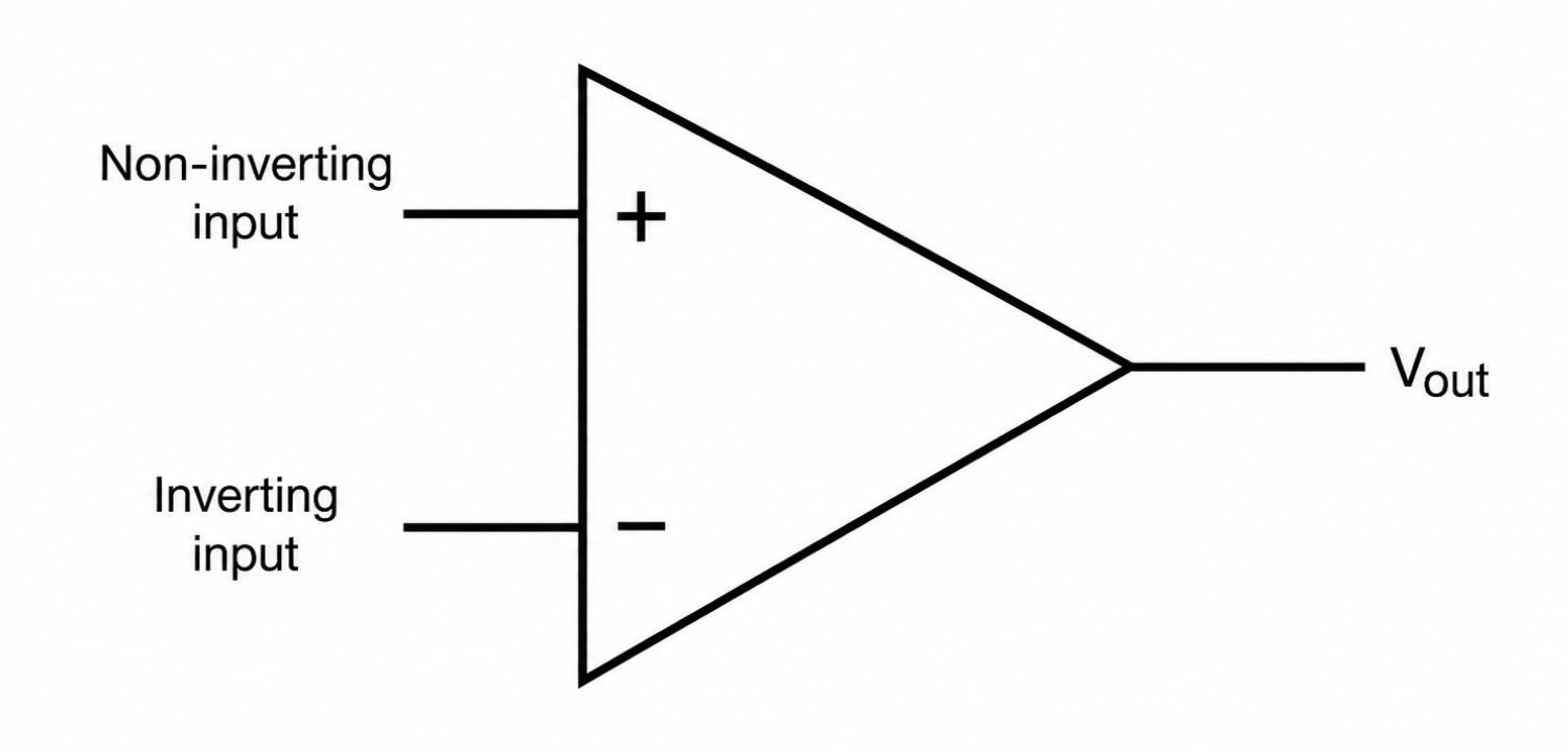
Figure: Op amp symbol diagram showing inverting input, non-inverting input, and output
Operational Amplifier Symbol Quick Reference
| Marking | Meaning |
|---|---|
| + | Non-inverting input |
| − | Inverting input |
| Output | Amplified signal |
| VS+ | Positive supply |
| VS− | Negative supply |
| Symbol Element | Function |
|---|---|
| Triangle shape | Represents amplifier, signal flows left to right |
| + terminal | Non-inverting input |
| − terminal | Inverting input |
| Tip of triangle | Output (Vout) |
| Vertical lines (if shown) | Power supply rails, VS+ and VS− |
How to Read an Op Amp Symbol in a Schematic
Theory aside, most engineers need to recognize the symbol fast inside a real circuit. Three configurations cover almost every case a designer will encounter early on.
Example 1: Voltage Follower
Output feeds directly back to the inverting input. No gain, used as a buffer for high impedance sources.
Example 2: Inverting Amplifier
Input signal connects through a resistor to the inverting input. A feedback resistor, which you can read about in our resistor symbol guide, sets the gain. Non-inverting input is grounded.
Example 3: Comparator Circuit
One input is a fixed reference voltage, the other is the signal. No feedback path. Output swings between supply rails based on which input is higher.
In all three, the same triangle symbol appears; only the connections change, which is why context matters more than the shape itself.
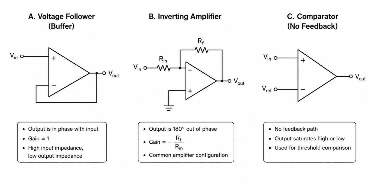
Figure: Op amp schematic examples showing voltage follower, inverting amplifier, and comparator wiring
Common Mistakes When Reading Op Amp Symbol
| Mistake | Fix |
|---|---|
| Assuming no power pins means no power needed | Always check datasheet for VS+ / VS− or +V/Gnd |
| Confusing op amp with comparator by shape alone | Check for feedback path, not just symbol shape |
| Swapping inverting and non-inverting pins when reading from datasheet vs textbook | Confirm pin numbers against the specific package, not memory |
| Ignoring single-supply limitations | Check output swing range before assuming dual-rail behavior |
Op Amp Symbol Inverting vs Non-Inverting Input
The + and − marks on the input pins are the most important detail on the symbol. They determine output phase, not voltage polarity.
The Inverting Input (−)
A signal applied to the inverting input produces an output 180° out of phase. Positive input voltage swing produces negative output swing, relative to the reference point.
The Non-Inverting Input (+)
A signal applied to the non-inverting input produces an output in phase with the input. No phase flip occurs.
What the Plus and Minus Signs Really Mean in Op Amp
The signs do not indicate DC polarity or voltage level. They indicate which input path causes phase inversion at the output. This is a common point of confusion for new designers.
Equation:
Vout = A * (V+ − V−)
Where A is open loop gain, V+ is the non-inverting input voltage, and V− is the inverting input voltage.
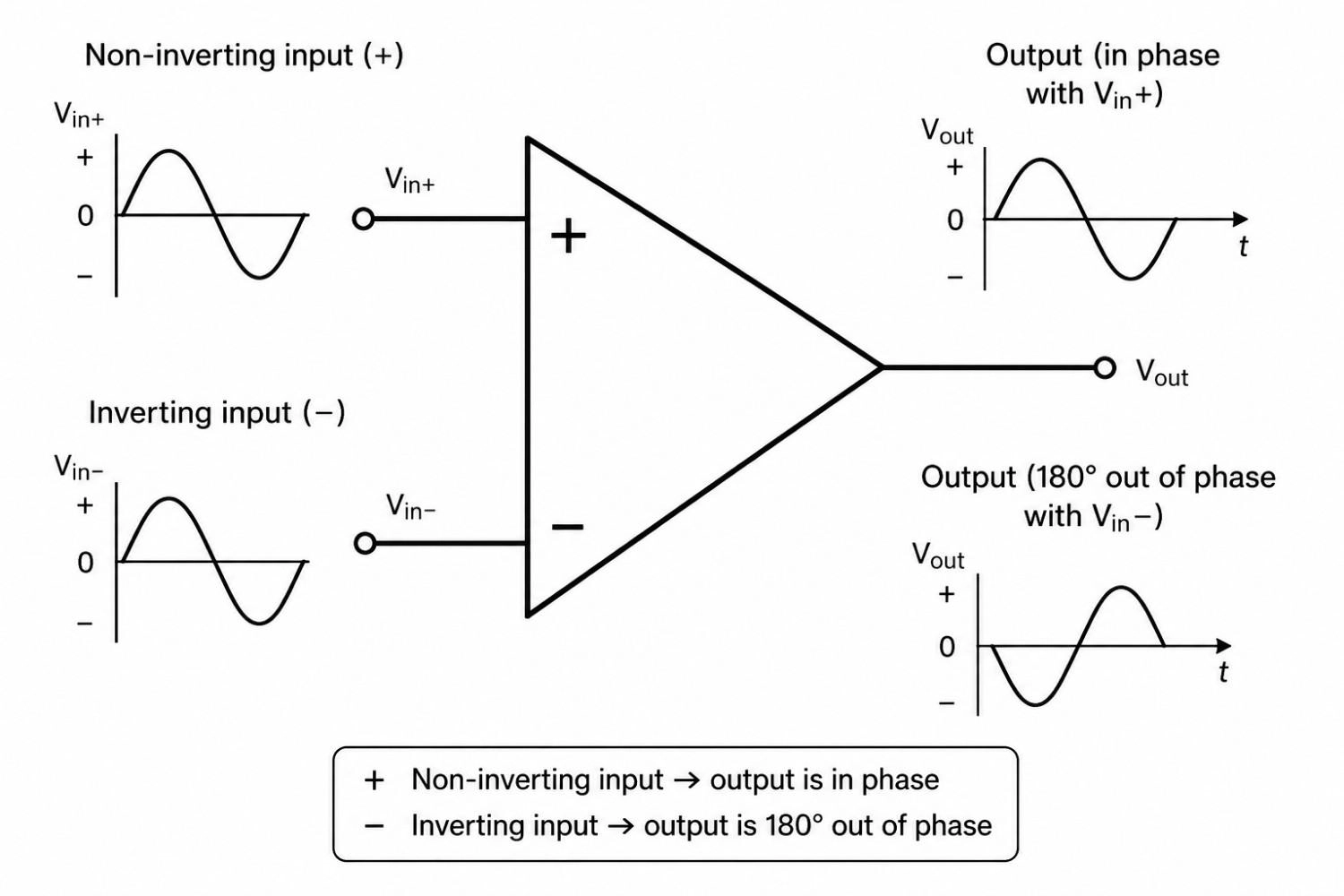
Figure: Op amp symbol showing signal path from inverting and non-inverting inputs to output with phase result
| Input | Sign | Output Phase | Typical Use |
|---|---|---|---|
| Non-inverting | + | In phase | Voltage follower, non-inverting amp |
| Inverting | − | 180° out of phase | Inverting amp, summing circuit |
Understanding Op Amp Power Supply Pins
Power pins are the most overlooked part of the op amp symbol, and the most common source of confusion when reading real schematics.
VS+ and VS− in Operational Amplifier
VS+ and VS− are the supply rails that power the op amp internally. They are separate from the signal inputs and output.
Without these connections, the op amp cannot operate, regardless of how the signal pins are wired. In practical designs, adding a bypass capacitor in PCB layout close to these supply lines is essential to filter out power supply noise.
Single-Supply vs Dual-Supply Op Amps
- Dual-supply op amps use a positive and negative rail (for example +15V and −15V), allowing output swing above and below ground.
- Single-supply op amps use +V and Gnd (or 0V), common in battery-powered and automotive designs, but limit output swing to the positive range.
Why Power Pins Are Often Hidden
In simplified schematics, especially in textbooks and tutorials, VS+ and VS− are frequently omitted to reduce clutter when the supply is implied or covered elsewhere in the design.
Always verify power pin connections against the datasheet before assuming a schematic is complete.
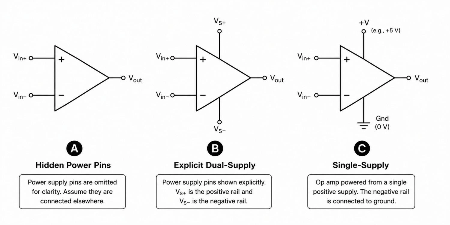
Figure: Three op amp symbols comparing hidden power pins, explicit VS+ VS- rails, and single-supply configuration
| Configuration | Pins Used | Typical Application |
|---|---|---|
| Dual supply | VS+, VS− | Audio, instrumentation, precision analog |
| Single supply | +V, Gnd | Battery powered, automotive, sensors |
| Hidden rails | Implied, not drawn | Simplified teaching diagrams |
Op Amp vs Comparator Symbol
Comparator and op-amp diagrams often use the same triangle symbol, which makes circuit context and feedback connections the key distinction, not the symbol shape.
| Feature | Op Amp | Comparator |
|---|---|---|
| Symbol | Triangle | Triangle (often identical) |
| Operating mode | Linear, with feedback | Saturated, output at rail levels |
| Feedback | Usually present | Usually absent |
| Output behavior | Proportional to input difference | Binary high or low |
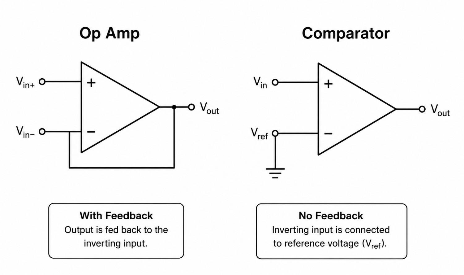
Figure: Comparison of op amp symbol and comparator symbol showing the feedback path versus reference voltage input
741 Op Amp Pinout: Mapping the Symbol to Real Pins
Understanding the Classic 741 Op Amp Pinout
The 741 remains the most recognized educational op amp. Its classic DIP-8 pinout includes inverting input, non-inverting input, output, and positive and negative supply pins, plus offset null pins not required for basic use.
Mapping 741 Op Amp Symbol Pins to Physical Pins
The schematic symbol shows function (+ input, − input, output). The physical IC pinout shows location. Both must be cross-referenced when wiring a real board, since pin numbers vary by manufacturer and package type.
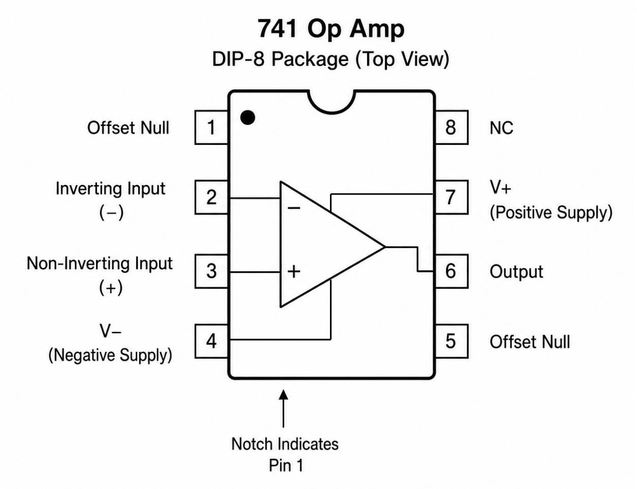
Figure: 741 op amp DIP-8 package top view showing pin 2 inverting input, pin 3 non-inverting input, pin 4 negative supply, pin 6 output, pin 7 positive supply
| Pin | Name | Function |
|---|---|---|
| 2 | Inverting Input | (−) |
| 3 | Non-Inverting Input | (+) |
| 4 | V− | Negative Supply |
| 6 | Output | Amplified Signal |
| 7 | V+ | Positive Supply |
From Op Amp Schematic Symbol to PCB Footprint
- Schematic vs. Footprint: The schematic symbol defines the component's function (inverting/non-inverting inputs, output), while the PCB footprint dictates the physical package (pin spacing, pad size, and orientation).
- Preventing Errors: Pin orders must match exactly between the schematic and the footprint. Mismatched mappings often escape simulation checks and are only discovered after fabrication, which is costly and difficult to fix.
- Verification: Before fabrication, verify three key elements: schematic symbol pin labels, footprint pin assignments, and the actual package pinout from the datasheet.
- Package Switching: Always verify pin configurations when changing package types (e.g., from through-hole DIP-8 to surface-mount SOIC-8), as physical spacing and pin orientation often differ even if the pin count remains the same.
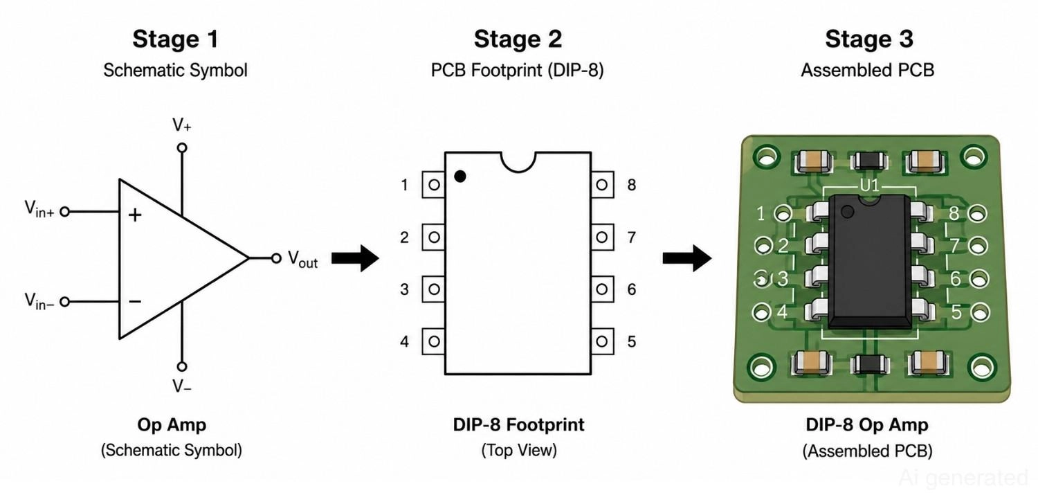
Figure: Showing progression from op amp schematic symbol to DIP-8 footprint to assembled PCB
FAQs about Op Amp Symbol
Q: How do you identify Pin 1 on physical DIP-8 and SOIC-8 op amp packages?
On standard DIP-8 and SOIC-8 packages, a small notch on one end of the plastic body or a circular dot adjacent to a corner indicates Pin 1. Pin numbering always runs counter-clockwise starting from Pin 1 when looking at the package from the top down.
Q: What is the typical input impedance of an ideal operational amplifier?
An ideal op amp has infinite input impedance, meaning it draws zero current from the input signal source. In real-world circuits, this prevents the amplifier from loading down the preceding circuit stage.
Q: What are the offset null pins on the 741 op amp used for?
The offset null pins (typically pins 1 and 5 on the 741 DIP-8 package) are used to nullify small, unwanted DC voltage offsets between the inputs. A potentiometer can be connected across them to balance the internal differential amplifier stage.
Q: Why do some multi-channel op amp packages share a single schematic designator prefix?
Multi-channel ICs (such as dual or quad op amps) are represented as individual schematic gates (labeled U1A, U1B, etc.) to keep layout paths readable. These gates share a single designator prefix because they exist inside a single physical integrated circuit package.
Q: What happens if the positive and negative power supplies are connected in reverse?
Reversing the power supply connections forward-biases the internal ESD protection diodes and substrate junctions. This usually results in immediate, catastrophic thermal runaway and permanent silicon damage, rendering the IC unusable.
Conclusion
The op amp symbol looks simple, a triangle with two inputs and one output, but misreading the + and − pins or missing power connections causes real circuit errors. Knowing inverting vs non-inverting behavior, recognizing hidden power pins, and distinguishing op amps from comparators covers most real-world schematic reading needs. The 741 pinout example bridges symbol theory to physical wiring. Once the symbol is clear, moving from schematic to footprint to a working board becomes a much shorter step.
Popular Articles
• How to Create a Bluetooth-Controlled Car With Arduino: A Step-by-Step Guide
• How to Design and Assemble a Reliable ESP32 Module PCB on a 2-Layer Board
• The Ultimate Guide to Relay Symbol: Coil, Contacts, Diagrams, and Circuit Applications
• How to Identify SMD LED Polarity: Markings, Testing, and PCB Tips
• The Ultimate Guide to PCBA: Process,Types and Techniques for the Electronics Enthusiast
Keep Learning
Arduino LED Driver Tutorial: Control More LEDs with 74HC595 and MAX7219
Arduino GPIO pins run out quickly in larger LED projects. By utilizing dedicated LED drivers and expansion ICs, you can drastically reduce pin usage, eliminate processor-heavy multiplexing loops, and simplify display wiring. In this guide, you will learn the operational architecture, wiring configurations, cascading techniques, and optimization strategies for the 74HC595 shift register and the MAX7219 LED driver. Why Arduino Projects Need LED Driver ICs Arduino GPIO and Current Limitations An ATmega32......
How to Create a Bluetooth-Controlled Car With Arduino: A Step-by-Step Guide
This tutorial walks through the complete engineering and implementation of a two-wheel Bluetooth RC car with an Arduino Nano module on a specially designed PCBA (Printed Circuit Board Assembly). While many hobbyists start by wiring motors and Bluetooth modules with jumper cables on a breadboard, this approach is prone to disconnection and signal noise. This guide upgrades that process by teaching you how to design a professional mainboard. Key Design Features Controller: Arduino Nano used as a plug-in......
Fiducial Marks in PCB and SMT Assembly: A Complete Guide to Accuracy and Design Rules
Modern Printed Circuit Boards (PCBs) are complex, integrating high-density components like 0.4mm pitch Ball Grid Arrays (BGAs), 0201 passives, and fine-pitch Quad Flat No-Lead (QFN) packages. In this advanced manufacturing environment, achieving placement accuracy measured in micrometers is crucial. A significant challenge in automated manufacturing is how pick-and-place machines, which handle thousands of components per hour, precisely locate the PCB. A board on a conveyor system is never in the perf......
Alternating Current vs Direct Current (AC vs DC): What's the Difference?
Electric current flows in two primary forms: alternating current (AC) and direct current (DC). AC periodically reverses direction, while DC flows steadily in one direction. AC powers the industrial and residential electrical grids, while DC powers batteries, electric vehicles, and nearly all modern consumer electronics. Understanding the core differences between AC and DC matters when designing power supplies, selecting electronic components, or laying out printed circuit boards (PCBs). This guide com......
Arduino LED Multiplexing Tutorial: Control More LEDs with Fewer Pins
The Arduino Uno is a powerful tool for prototyping, but driving multiple LEDs directly quickly exhausts its 20 GPIO pins and its 200 mA absolute maximum package current limit. To bypass these hardware bottlenecks, engineers and hobbyists use LED multiplexing to scale display outputs efficiently without upgrading the microcontroller. In this guide, you will learn the core principles of LED matrix scanning, Charlieplexing, refresh timing, ghosting fixes, and practical Arduino code without relying on any......
Op Amp Symbol Explained: Pinout, Polarity, and Power Pins
The op amp symbol is one of the most common shapes in analog schematics: a triangle with two inputs and one output. Reading it correctly, knowing which pin is inverting, which is non-inverting, and how power connects, is the first skill needed before building any amplifier circuit. Standard op amp symbols include a non-inverting input, an inverting input, an output, and power supply connections that may be shown or hidden depending on schematic style. The common symbol convention uses a triangle with ......