KiCad MCP: How to Design a PCB with Claude Code [Step-by-Step]
15 min
- Introduction
- How Does Claude Code Design a PCB in KiCad Using MCP?
- Claude KiCad MCP Example: An XL4015 5 A Buck Converter PCB
- How to Set Up a KiCad MCP Server Safely
- KiCad MCP Workflow: From Schematic to Finished Board
- KiCad MCP Problems: What Went Wrong and How It Was Fixed
- From KiCad MCP Design to JLCPCB Order: Gerbers, BOM, and Parts
- Conclusion
- FAQs About KiCad MCP
Key Takeaways
- Claude can design PCBs in KiCad: By connecting Claude to KiCad through an MCP server, you can use AI to create and modify PCB designs. In this project, Claude helped turn a 5 A XL4015 buck converter netlist into a two-layer, 63 × 33 mm PCB layout with zero ERC violations and zero DRC errors after minor initial fixes.
- Set up Claude securely: Use a KiCad MCP server that starts in read-only mode. Review the server code before installing it, connect through stdio, and allow editing only in a dedicated project folder tracked with Git.
- Check the circuit before designing: Before creating the schematic, reviewing the reference design against component datasheets revealed four issues. These included an incorrect ground connection on the XL4015 VC pin and a 78L05 regulator that could not handle the circuit's maximum input of 36 V.
- Don't rely on ERC alone: KiCad's Electrical Rules Checker (ERC) did not catch a connection error between the current-sense and current-limit set-point nets. A pin-by-pin comparison of the exported netlist revealed the problem and helped verify all 16 nets.

Introduction
What if you could ask Claude AI to design a PCB in KiCad and watch it create the schematic, place components, and route the board? With a KiCad MCP server, Claude can interact directly with KiCad 10, turning design instructions into an actual PCB layout.
But how well does it work on a real circuit? To find out, we used Claude to design a 5A XL4015 buck converter PCB, from schematic creation to a two-layer board layout. Along the way, we explored what Claude can handle on its own, where it makes mistakes, and why human verification is still important.
In this article, we'll walk through how Claude connects to KiCad, how to set up the MCP server safely, and what happened when we put AI-assisted PCB design to the test.
In this guide, you will learn:
- How Claude AI connects to KiCad to design and edit PCBs
- How to safely set up a KiCad MCP server
- Step-by-step design: from schematic generation to finished board layout.
- Which errors passed ERC, and how to verify the board
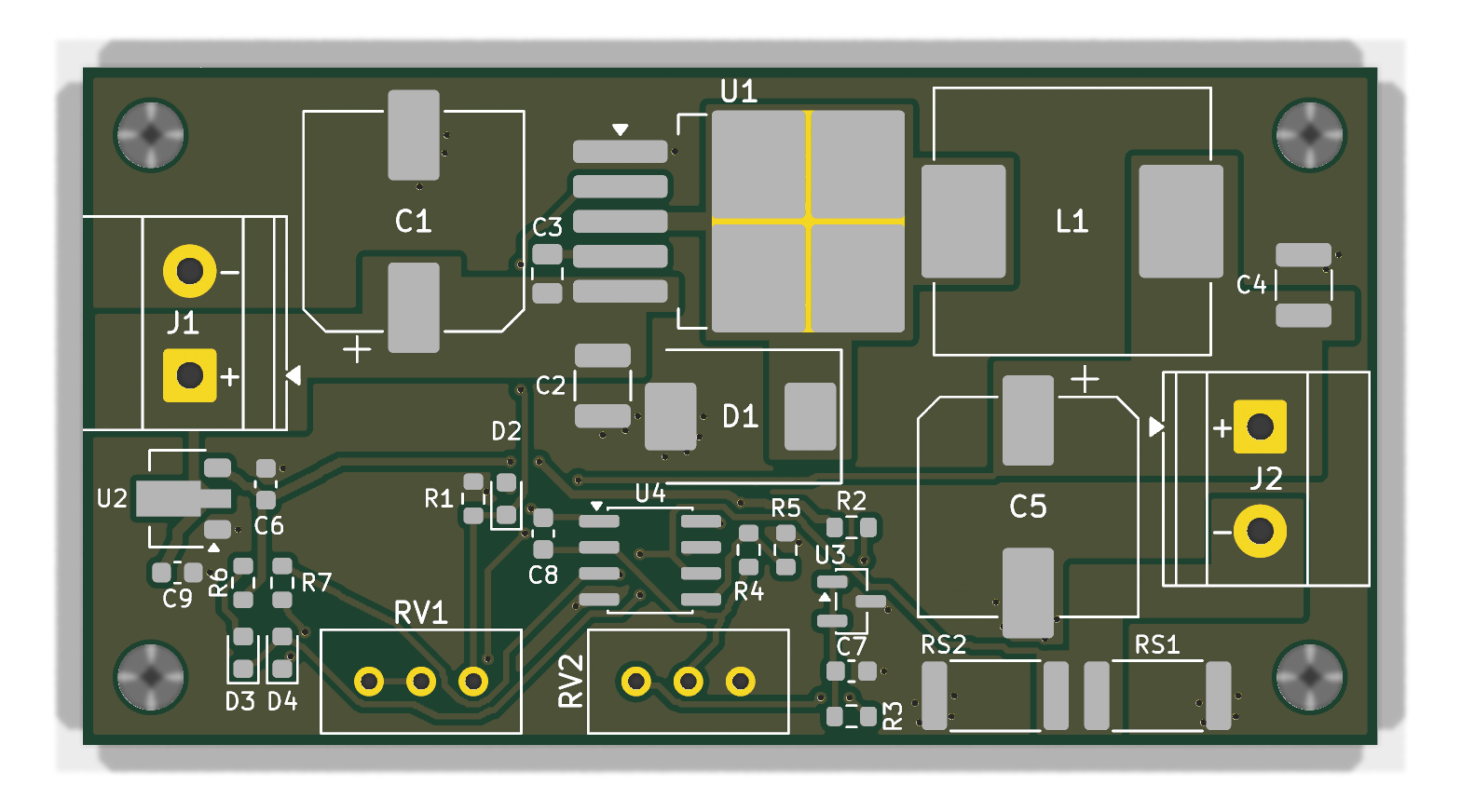
Figure: 3D view of the XL4015 buck converter PCB designed with Claude in KiCad 10
How Does Claude Code Design a PCB in KiCad Using MCP?
Claude Code can design a PCB in KiCad by using the Model Context Protocol (MCP) to communicate with KiCad's design tools.
The MCP server acts as a bridge, allowing Claude Code to read project files, create schematics, place components, route traces, and perform design checks. Instead of simply generating PCB design suggestions, Claude Code can make actual changes to the KiCad project.
However, the operations it can perform depend on the MCP server, and the resulting design still requires engineering verification.
A KiCad MCP setup has three parts:
- AI client: Claude Code or the Claude desktop app, which decides which tool to call and with what values.
- MCP server: A local program that exposes KiCad actions as tools, such as building a schematic, moving a footprint, or running DRC.
- KiCad: The KiCad editor is accessed via the KiCad API while the project is open, and via kicad-cli for exports and design checks.
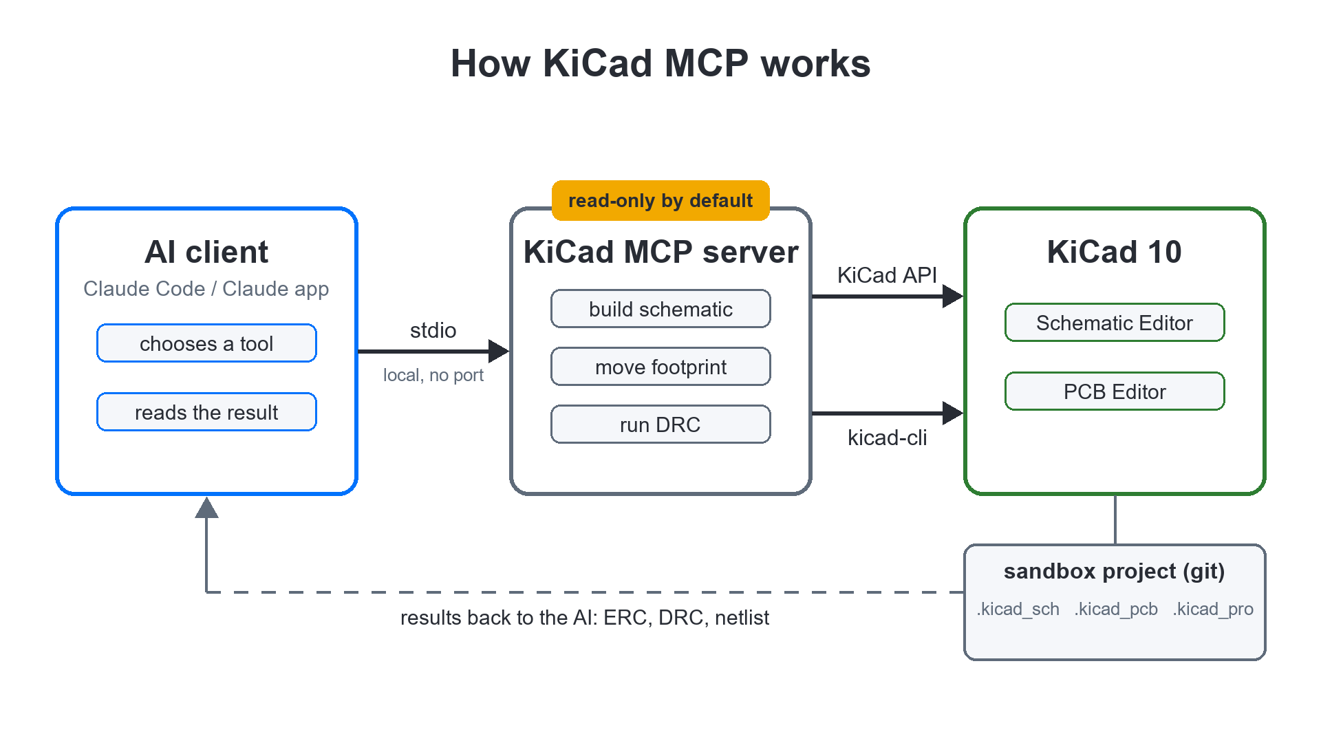
Figure: How KiCad MCP works
KiCad MCP is not a single product. Several open-source servers exist, and they differ in how much of your project they can change. It belongs to the broader group of AI tools for PCB design and works directly with your KiCad project.
Claude KiCad MCP Example: An XL4015 5 A Buck Converter PCB
In one working session, Claude and a KiCad MCP server produced a two-layer, 63 × 33 mm XL4015 buck converter board with 0 ERC violations and 0 DRC errors. It redesigns a common 5 A CC/CV module and has not yet been fabricated or bench-tested.
| Parameter | Value |
|---|---|
| Converter IC | XL4015E1 buck converter, 180 kHz |
| Input | 8–36 V DC, the XL4015's rated input range |
| Output | 1.25–32 V, set with trimmer RV1 |
| Output current | Rated 5 A; the current-limit trimmer (RV2) adjusts up to about 5.9 A |
| Current control | LM358 current loop on a low-side shunt, TL431 2.5 V reference |
| Indicators | 3 LEDs: CC mode, charging, and full |
| Board | 63 × 33 mm, 2 layers, 1 oz copper, 4 × M3 holes |
| Status | DRC-clean in KiCad 10.0.4; not fabricated or bench-tested |
Design Fixes Over the Reference XL4015 Module
Before any schematic existed, a datasheet review of the reference module found four problems. The fix sizes the input side to the XL4015's maximum operating input of 36 V, rather than the narrower range listed on the seller's page.
The review came first because KiCad MCP builds the schematic from the given netlist.
| Problem in the Reference Module | Risk | Fix in This Design |
|---|---|---|
| XL4015 VC pin (pin 4) tied to GND | Departs from the datasheet, which requires a 1 µF capacitor from VC to VIN | C3, 1 µF from VC to VIN |
| 78L05 regulator, rated for 30 V input | Below the XL4015's 36 V maximum operating input | BL8078 LDO, rated for 40 V input |
| Single 0.05 Ω shunt | Dissipates 1.25 W at 5 A | Two 0.1 Ω, 2 W resistors in parallel, about 0.63 W each |
| 35 V bulk capacitors | Below the XL4015's 36 V maximum operating input | 220 µF, 50 V capacitors |
How to Set Up a KiCad MCP Server Safely
Choose a server that is read-only by default, install it from a copy you have reviewed, connect it over stdio, and confine it to one project folder under git. Then enable the KiCad API so the server can reach the open editor.
Choosing a KiCad MCP Server: Access Comparison
Which KiCad MCP Server should you use?
The main difference between servers is what they can change by default:
| Server | Default Access | Board Design Support | Note |
|---|---|---|---|
| oaslananka/kicad-mcp-pro | Read-only review tools | Yes, in its build (write) profile | Write and manufacturing profiles are explicit opt-ins |
| Seeed-Studio/kicad-mcp-server | Mainly analysis: ERC, DRC, net tracing | Limited; schematic editing is experimental | Suited to design review |
| mixelpixx/KiCAD-MCP-Server | Full read and write | Yes, the widest feature set | Grants write access from the start |
| lamaalrajih/kicad-mcp | Read and partially edit | Partial | No updates for about a year at the time of this build |
This build used kicad-mcp-pro, because its read-only default limits what an AI error can change.
Installing KiCad MCP and Connecting It to Claude
The installation followed five steps (copy and paste this step directly into Claude, and it will manage the installation for you):
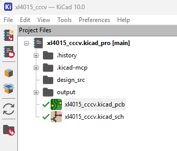
Figure: KiCad project tree of the sandbox folder used by the KiCad MCP server
- Review the code first: The targeted review checked for network calls and telemetry, the subprocesses it starts (kicad-cli, git, and ngspice only), and whether file paths remain within the workspace root.
- Install a pinned copy: The reviewed release was copied into a private repository and installed from there, using the hash-locked dependency file.
- Register it with Claude Code over stdio: stdio does not open a network port, so only the local client can reach the server.
- Confine it to one sandbox folder under git: Turn on the server's build (write) profile only for this folder. Each change the AI makes can then be inspected with git and reverted if needed.
- Enable the KiCad API: In KiCad, open Preferences > Plugins and select Enable KiCad API.
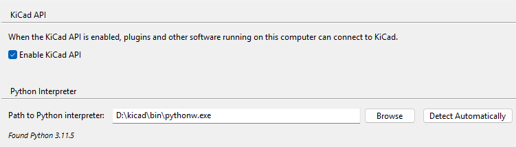
Figure: KiCad 10 preferences with the Enable KiCad API option selected
KiCad MCP Connection Problems and Fixes
These four problems blocked the connection during the build:
| Symptom | Cause | Fix |
|---|---|---|
| The server cannot connect, with no error message | A second KiCad window, opened for another project, holds the API connection | Keep one KiCad instance open |
| API calls stop responding | A modal dialog, such as "File Open Warning," is waiting in KiCad | Close the dialog |
| Board-editing tools are missing | The PCB Editor does not have the board open | Open the board in the PCB Editor |
| The server cannot reach KiCad at all | The KiCad API is disabled | Enable it under Preferences > Plugins |
KiCad MCP Workflow: From Schematic to Finished Board
The design went from netlist to finished board in four steps. In each step, the AI did the editing, and a check confirmed the result before the next step began.
Step 1: Generating the KiCad Schematic from a Netlist
Claude built the schematic with one MCP call, sch_build_circuit, from a 16-net netlist. Each pin received a short wire stub and a named net label, so the nets connect by name.
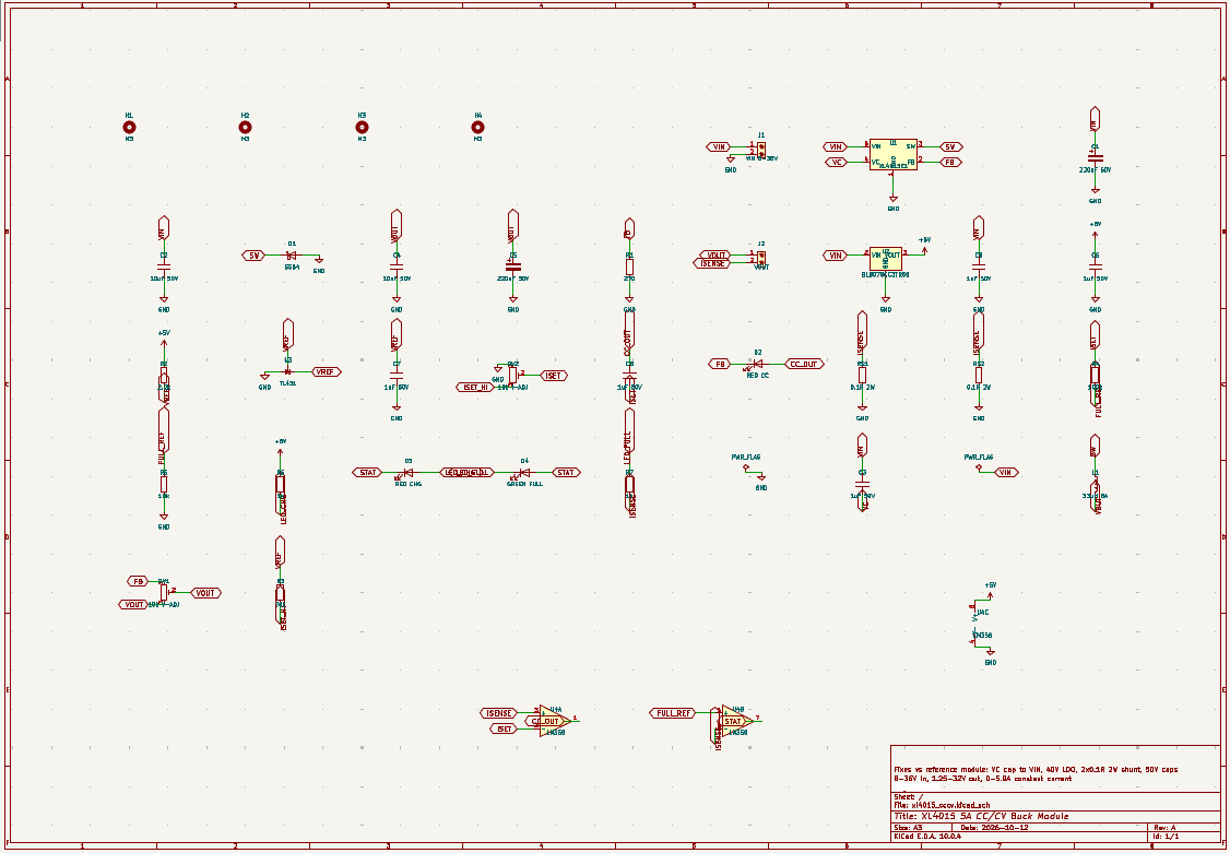
Figure: Schematic generated with KiCad MCP for the XL4015 5 A CC/CV buck converter
Two problems appeared during this step:
- Overlapping LM358 units: During automatic schematic layout, Claude Code placed the LM358 schematic units on top of each other. The MCP server also struggled to identify the pins belonging to each unit.
- Overlapping net labels: Two overlapping labels accidentally connected the current-sense (ISENSE) and current-limit set-point (ISET) nets. KiCad's Electrical Rules Checker (ERC) only raised a warning, not flagging the connection as an error. A pin-by-pin comparison of the exported netlist revealed the mistake, allowing it to be corrected.
The final schematic passed ERC with 0 violations, and the exported netlist matched the intended one on all 16 nets.
Step 2: Sizing the Board and Placing Components
The component courtyards required about 1,500 mm², exceeding the 1,272 mm² of the reference module's 50.5 × 25.2 mm outline. The board grew to 63 × 33 mm with four M3 holes.
Placement was planned offline using a script that checked for overlaps and generated a preview using the ratsnest. The positions were then applied live in KiCad with the pcb_move_footprint tool.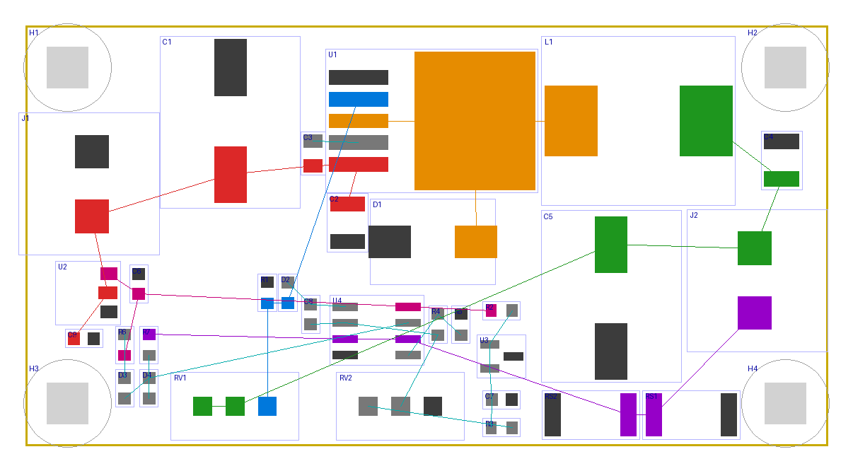
Figure: Placement plan for the XL4015 buck converter PCB, with courtyards and ratlines
The layout follows the PCB layout principle of a short, direct power path:
- Power flow, left to right: J1 > C1 > XL4015 > switching node > L1 and D1 > output capacitors C4 and C5 > J2.
- Switching loop: The input ceramic capacitor C2 sits between the XL4015 VIN pin and the anode of catch diode D1, which keeps the high-current switching loop small.
- Current sense: The shunt resistors sit on the return path, and the trimmers sit on the bottom edge for access.
Step 3: Routing the Power and Feedback Nets
The KiCad MCP server did not include an autorouter, so Claude Code created its own basic routing tool in Python. It used the A* pathfinding algorithm to find routes on a 0.1 mm grid across both PCB layers. For high-current connections, Claude used copper pours instead of narrow traces to provide wider paths for current flow:\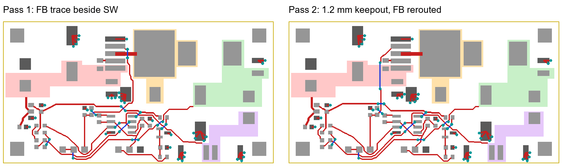
Figure: FB trace beside the SW node in pass 1
- Copper pours: VIN, SW, VOUT, and the current-sense path.
- Ground: A GND plane on the bottom layer and a GND fill on the top layer.
The first pass routed the feedback (FB) trace right beside the switching node, where switching noise can couple into the regulation loop. A 1.2 mm keepout around SW for analog nets fixed it, in line with standard PCB routing rules. FB now leaves to the left and passes under VIN on the bottom layer.
Step 4: Running KiCad DRC and Cleaning Up the Silkscreen
The first design rule check reported 7 copper-to-edge errors. The router had used a 0.35 mm edge clearance, while the board rule was 0.5 mm. After the router was corrected and the board rerouted, the final DRC showed 0 errors, 0 unconnected items, and 0 schematic-parity issues.
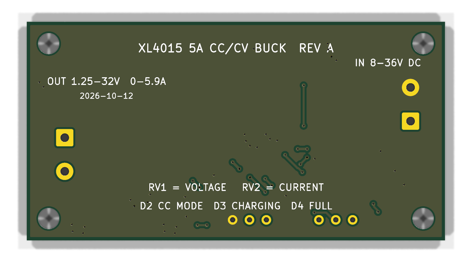
Figure: Bottom side of the KiCad MCP board with the silkscreen legend for ratings
A label-placement script then moved each reference designator clear of pads and other silkscreen. Silkscreen warnings fell from 47 to 2, both from terminal-block bodies at the board edge. The bottom legend lists the ratings, the trimmer roles, and the LED meanings.
KiCad MCP Problems: What Went Wrong and How It Was Fixed
The AI or the server caused seven distinct issues during the build. A check caught each one: the netlist comparison, DRC, a layout review, or a direct parts query.
| Problem | Effect | Fix |
|---|---|---|
| Auto-layout stacked all three LM358 units in one spot | Overlapping pins created unintended connections | Each unit is placed at its own free coordinates; the netlist is rechecked, 16/16 nets |
| The server could not wire multi-unit parts | LM358 units stayed unconnected | 9-line patch to the private server copy so it resolves pins on every unit |
| Net-label collision | ISENSE is shorted to ISET, while ERC only warned | Found by the pin-for-pin netlist comparison |
| FB trace routed beside SW | Switching noise could couple into the feedback | 1.2 mm keepout for analog nets, then rerouted |
| Router used 0.35 mm edge clearance | 7 DRC copper-to-edge errors against a 0.5 mm rule | Router corrected, and board rerouted |
| Server's part search returned unreliable results | Part matches could not be trusted | Direct query of the JLCPCB parts data |
| Placement batch ran twice | Board outline drawn twice | Duplicate outline removed |
Why ERC Is Not Enough for AI-Generated PCB Designs: Verify the KiCad Netlist
ERC checks electrical rules such as unconnected pins and conflicting outputs. It does not know which pins you intended to connect, so a short between two valid nets can pass. Add these checks after ERC:
- Write down the intended netlist: List every net and every pin on it before the AI builds anything.
- Export the netlist with kicad-cli: Use the schematic the AI generated, not the one you planned.
- Compare every net, pin-for-pin: In this build, 16 of 16 nets matched after the ISENSE short was fixed.
Note
Zero DRC errors mean the layout meets its rules. It does not confirm that the schematic matches your intent or that the pin order matches the part order, so complete the netlist and pinout checks before generating manufacturing files.
From KiCad MCP Design to JLCPCB Order: Gerbers, BOM, and Parts
The design is not ready to order yet: the Gerber, BOM, and CPL files have not been generated because the server's manufacturing profile is still off. The parts are already chosen with LCSC numbers, using JLCPCB Basic parts where possible.
The key parts, checked in the JLCPCB Parts Library:
- XL4015E1 (C51661): buck converter IC
- LM358DR2G (C7950): current-loop op-amp, a Basic part
- BL8078CC3TR50 (C692269): 5 V LDO, rated for 40 V input
- TL431 (C181103): 2.5 V reference
- CYA1265-33UH (C19268671): 33 µH, 6 A inductor
- SS54 (C5204950): catch diode
- 0.1 Ω, 2 W, 2512 (C160587): current-sense shunt, two in parallel
The remaining steps are the standard KiCad export flow.
Generate the Gerber and drill files with the KiCad Gerber export guide, then export the BOM and CPL files with the KiCad BOM and CPL guide for SMT assembly.
Conclusion
Claude Code can turn a netlist into a complete, DRC-clean PCB layout in KiCad using MCP, but human verification is still essential. In this project, Claude Code handled the PCB design, while manual netlist and datasheet checks helped identify and correct errors the AI missed.
Use KiCad MCP for schematic entry, placement, and rule fixes, and keep the engineer on netlist comparison, pinout checks, and layout review. This split keeps the speed of AI-driven editing while still checking every connection against the design intent.
Once your design is verified, upload your files to JLCPCB to get an instant quote.

FAQs About KiCad MCP
Q: Can Claude Design a PCB in KiCad on Its Own?
Not completely. While Claude can generate the schematic and board layout, engineer review through netlist comparison and datasheet checks remains essential to catch subtle errors that pass ERC.
Q: Which KiCad MCP Server Should I Use?
Start with a server that is read-only by default, such as kicad-mcp-pro. Enable write access only for one sandbox project tracked in git.
Q: Does the KiCad MCP Server Include an Autorouter?
Not the server used here. The traces came from a small Python grid router that Claude wrote during the session, with copper pours for the power nets.
Q: Can a Board with Zero DRC Errors Go Straight to Manufacturing?
Not on its own. DRC checks the layout against its rules; it does not check that the schematic matches your intent or that pinouts match your parts.
Q: Does KiCad MCP Work with KiCad 10?
Yes. This build used KiCad 10.0.4 with the KiCad API enabled under Preferences > Plugins. Check each server's compatibility notes, because support varies by version.
Popular Articles
• AI Tools for PCB Design: Which Tool Fits Your Workflow Stage?
• AI PCB Design: From Prompt to PCB with EasyEDA Pro
• GPT-6 Astra PCB Design in KiCad: From Brief to Verified Native Project
• GPT-6 Astra PCB Design in EasyEDA Pro: What Worked, What Failed, and What We Learned
• How to Design Your Own Keyboard PCB: From Layout to Firmware
Keep Learning
KiCad MCP: How to Design a PCB with Claude Code [Step-by-Step]
Key Takeaways Claude can design PCBs in KiCad: By connecting Claude to KiCad through an MCP server, you can use AI to create and modify PCB designs. In this project, Claude helped turn a 5 A XL4015 buck converter netlist into a two-layer, 63 × 33 mm PCB layout with zero ERC violations and zero DRC errors after minor initial fixes. Set up Claude securely: Use a KiCad MCP server that starts in read-only mode. Review the server code before installing it, connect through stdio, and allow editing only in a......
Claude Code PCB Design: Can It Build a Real Board in EasyEDA Pro?
Key Takeaways Claude Code PCB design: Using Claude Opus 5.5 and EasyEDA Pro 3.2.149, I converted a 47-component, three-page schematic from a PDF into a fully routed, two-layer PCB with zero DRC errors. EasyEDA Pro integration: The EasyEDA API skill connects Claude Code to EasyEDA Pro through a local bridge server and the Run API Gateway extension. This allows Claude to control the editor via JavaScript, with a 30-second timeout per API call. Design verification: A successful API response doesn't alway......
How to Design a PCB with Flux.ai (Step-by-Step Guide)
Key Takeaways This step-by-step Flux PCB design tutorial demonstrates the complete workflow by creating a compact 15 × 15 mm USB 2.0 hub, refining the layout, routing high-speed differential traces, and preparing manufacturing files for JLCPCB PCB fabrication and assembly. We are all hearing news; new AI models are being released every month. And it has finally reached the schematic editor. Flux.ai is a browser-based AI PCB design tool with a built-in AI agent that behaves like a junior hardware engin......
AI Tools for PCB Design: Which Tool Fits Your Workflow Stage?
AI tools can now assist with PCB architecture, schematic generation, component selection, placement, routing, and design verification. However, different tools target different stages of the PCB workflow. This guide compares AI tools for PCB design based on what they actually do, what inputs they require, and where they fit within a real engineering workflow. In this guide, you will learn: The 6 types of AI PCB tools and the input each one needs What AI PCB design tools do, compared stage by stage How......
AI PCB Design: From Prompt to PCB with EasyEDA Pro
Key Takeaways AI PCB design uses AI agents to automate schematic creation, component selection, layout, and verification inside a real EDA editor — not just generate images. The workflow connects EasyEDA Pro to an AI coding agent (Claude Code or Codex) through the EasyEDA API Gateway, the open-source API Skill, and a local bridge server. Setup takes about ten minutes and is fully local-first: designs, API calls, and intermediate code never leave your machine. Because the agent places real library part......
GPT-6 Astra PCB Design in KiCad: From Brief to Verified Native Project
Key Takeaways What OpenAI published: The launch page features a 15-second condensed clip of GPT-6 Astra performing PCB layout in KiCad. What the model did: It turned a four-line brief into a 44 × 34 mm, two-layer PCB, covering the circuit, footprints, component placement, routing, and a native two-sheet schematic. Where the work went: Placement and routing were only part of the work. Two linked schematic sheets, project-local libraries, and UUID-based links between 45 components and their footprints w......