Creating Clear and Professional Reference Designators for Better PCB Assembly
15 min
- Understanding Reference Designators in PCB Projects
- Why High-Quality Reference Designators Matter
- Best Practices for Reference Designator Placement and Styling
- Common Mistakes and How to Avoid Them
- From Design to Reliable Manufacturing
- JLCPCB's Expertise in Professional Reference Designator Implementation
- FAQ about PCB Reference Designators
- Conclusion
Key Takeaways
- Reference designators are essential for accurate PCB assembly, debugging, and maintenance.
- Use minimum 0.8 mm text height and 0.15 mm line width for clear silkscreen printing.
- Keep designators on solder mask with proper clearance from pads and vias.
- Maintain consistent font, size, and orientation across the board.
- For high-density designs, use an assembly drawing instead of crowded silkscreen.
- Always run DFM checks to avoid overlapping or missing labels.
Ever wonder about the little labels on a bare PCB, like "R47" or "C12", and why they are there? That little white writing is a reference designator, and it is one of the hardest workers in the whole electronics process. If not, an assembler would not know where to place each resistor, and a technician would have to reverse-engineer the entire board to diagnose a failure.

The thing is that while a reference designator may seem insignificant, they are the glue that holds your schematic, bill of materials, pick-and-place files, and the actual board together and makes them speak the same language. Once that language is understood, it is fast and without error. When it's messy, you lose parts, slow rework, and costly scrap. We will discuss what PCB reference designators are, why the quality of these designators is important, how to place them properly, some common pitfalls, and how good design translates to reliable manufacturing.
Understanding Reference Designators in PCB Projects
Let's get some basics out of the way first, before we move on to best practices. Once you grasp what the ref designator is, you make every decision downstream an easy decision.
What Reference Designators Are and Their Purpose
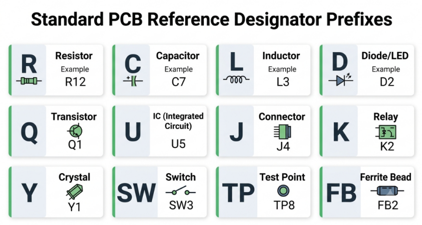
A reference designator, or designator, is a brief alphanumeric identifier that is used to uniquely identify each component on a printed circuit board. Each component is given a number, preceded by a letter to denote its type, such as R for resistors, C for capacitors, and U for integrated circuits. The letter prefixes do not reflect the arbitrary nature of the code. They use a long-established system of identifying families of components with a letter designator, as per IEEE 315 and ASME Y14.44. That is why you see a "PCB Component Code" such as Q in any schematic you read, indicating that it is a transistor.
The following table shows the most common prefixes that you will meet:
| Prefix | Component Type | Example |
|---|---|---|
| R | Resistor/potentiometer | R12 |
| C | Capacitor | C7 |
| L | Inductor/coil | L3 |
| D | Diode / LED | D2 |
| Q | Transistor | Q1 |
| U | Integrated circuit | U5 |
| J | Jack/connector (receptacle) | J4 |
| P | Plug (connector) | P1 |
| K | Relay | K2 |
| Y | Crystal/oscillator | Y1 |
| SW / S | Switch | SW3 |
| TP | Test point | TP8 |
| FB | Ferrite bead | FB2 |
| F | Fuse | F1 |
These labels serve a simple yet important function: they enable identification of each component on the board by people and machines, and facilitate their placement, testing, and replacement, without confusion.
Difference Between Schematic and PCB Reference Designators
One of the most frequent questions is, "Is the designator on the schematic the same as the designator on the board? They should be the same ideally, as R1 on the schematic should be physically the same as R1 on the PCB. This 1-to-1 association is the one that maintains the synchronization between your netlist, BOM, and layout.
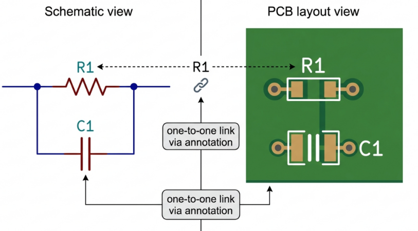
The schematic shows the reference designator by the symbol; it is for human readability when designing and reviewing. The same designator is printed on the silkscreen layer of the PCB next to the component's footprint and aids in its physical construction and subsequent service. With modern EDA tools such as EasyEDA and KiCad, these two views are automatically associated by annotation. In re-annotation or update of a schematic, the tool propagates changes to the layout so that the labels never get out of phase.
Why High-Quality Reference Designators Matter
You can easily overlook silkscreen labels. However, the PCB reference designator strategy you choose will directly impact cost, speed, and reliability throughout the product lifecycle.
Impact on Assembly Efficiency, Debugging, and Maintenance
Operators and inspectors refer to the BOM and placement documents continuously during the assembly process to prevent any errors. Clear, well-placed designators allow them to check part locations at a glance rather than having to search a cluttered silkscreen. Debugging is very dependent on the readability of the labels when something goes wrong:
- It is possible to detect U7 or C22 at a glance by a probing technician without the use of a magnifier.
- Rework operators can find the precise part to replace, and avoid the risk of touching the wrong joint.
- Field service teams can then cross-reference a failed part with the BOM and place the correct order.
Minutes per board can be lost due to a single ambiguous label, and that can mount up to significant time loss throughout the entire run when thousands of boards are involved.
Benefits for Quality Control and Long-Term Documentation
Reference designators are used at nearly every quality control point. A designator helps automated optical inspection (AOI) as well as humans check that the correct part is in the correct location in the correct orientation. Well-made designators also help to ensure long-term protection of your documentation. Many years after production, the repair depot might only be left with the physical board and a BOM. As long as the silkscreen is clear and complete, that board is usable; if the silkscreen is missing or unreadable, then this board is a puzzle. That's why it's advantageous to view a designator as a first-class designator, rather than a leftover, and why it is valuable for the whole product life cycle.
Best Practices for Reference Designator Placement and Styling
Let's get down to business. The bottom line is that good designators are a matter of disciplined placement, disciplined styling, and respecting the manufacturing tolerances of silkscreen.
Font Size, Orientation, and Readability Guidelines
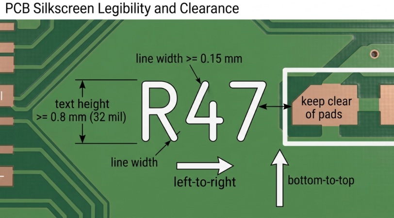
The size of the fonts and the thickness of the strokes are the first two things that lead to legibility. As a general guideline, text should be a minimum of 0.8 mm (32 mil) high and line width a minimum of 0.15 mm to enable the printing process to cleanly resolve each character. Going lower-risk is illegible text that inspectors can't read due to damage or blur. Here are some styling tips for flawless and professional results every time:
- Use one font only and make sure that it is clean: Changing fonts throughout the board makes it look unprofessional and will slow the reader down.
- All text displays should be in one of two directions: Left to right or bottom to top, but in the usual reading direction.
- Ensure that each designator is oriented straight: Not upside down or mirrored with respect to its two possible orientations.
- Write each label: Near the part they are associated with, but only one label next to each footprint.
- Keep characters consistent: None of the labels should be larger or smaller than the others.
The answer is that it's all about consistency. The eye locates information at a glance when all the labels follow the same rules.
Avoiding Overcrowding and Ensuring Silkscreen Clarity
Don't overcrowd a readable board. If designators overlap pads, vias, and other designators, the printer either omits the text or smears the text. Provide a small, clear, non-copper and non-drilling region around each label. There are a few habits that will help to keep silkscreen clean:
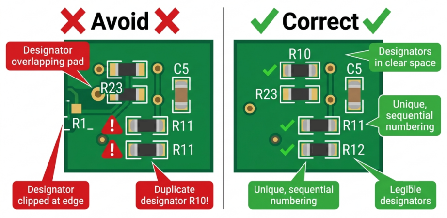
- Shove labels off pads and into unused board space, and maintain association.
- Try not to cluster several designators in a small area of passives.
- Allow space for breathing around connectors and tall pieces of text that may be shadowed.
If space is really limited, it is better to have the designator just outside the component outline, rather than try to squeeze it under.
Handling High-Density Boards and Fine-Pitch Components
High-density interconnect (HDI) boards and fine pitch parts represent a challenge – you can't easily place a readable label next to every 0201 resistor. If you attempt to fit full designators on a dense board, you'll end up with a cluttered board that is unreadable.
The answer is a designator map (also known as an assembly drawing or fab drawing). Instead of a crowded silkscreen on the board, you remove the silkscreen from the board and create an external reference document with each designator accompanied by a clean footprint outline. The map is used by the operators and AOI systems, and the board remains clutter-free. If you do have on-board text on dense layouts, use it for what is important for debugging: ICs, connectors, and test points; and for the tiny passives, look at the assembly drawing.
Common Mistakes and How to Avoid Them
Even bad designers make mistakes with silkscreen. It's the final thing you do before going live and is often rushed. These are the top offenders that cause the most grief.
Overlapping, Missing, or Inconsistent Designators
The most common issue is that text overlaps with pads/vias or other labels. When the parts are fabricated, the manufacturer usually clips the silkscreen away from any exposed copper, and any character on top of a pad just disappears, resulting in a partial or missing designator.
Be aware of these related issues:
- Missing designators: Parts were put in place, but not labeled, usually as a result of an added last-minute footprint.
- Duplicate designators: when these are copied and pasted to two parts and given the same designator "R10", this causes the BOM link to be broken.
- Inconsistent numbering: where there are gaps or parts not numbered in sequence, they are difficult to follow.
Perform a design rule check and a silkscreen-over-pad check on your design before you export it. Duplicate and gap detection is automatic with a quick re-annotation pass.
Poor Interaction with Solder Mask and Copper Features
A solder mask is required underneath for good adhesion of silkscreen ink and to maintain legibility. Adhesion is not good, and print quality is not good when text is placed on bare copper or over a large clearance gap. Be aware of these encounters:
- Don't route designators across board edges or slots where they'll be cut off.
- Do not have text over dense via fields because the text will be clipped.
- Provide ample solder mask under the text for a uniform deposit of the ink.
It is a good practice to check each silkscreen independently, i.e., only show copper and mask: this way, you will be able to see the places where conflicts occur, before they go to fab.
From Design to Reliable Manufacturing
Having a clean design file is only half the job. The manner in which your silkscreen is able to withstand the fabrication and surface finishing processes is what makes the difference in whether or not those labels will be legible on the end product.
DFM Considerations for Silkscreen and Reference Designators
Design for Manufacturability (DFM) Silkscreen is about respecting the process limits before sending files out. All fabricators have a minimum text height and a minimum line width, and if the text is smaller than either of these, it is marked or lost.
Maintain this checklist of DFM items:
- Ensure text height is at or above the minimum required by the fab (usually 0.8 mm), and line width is at or above about 0.15 mm.
- Make sure to leave space between silkscreen and pads, usually 0.1 mm or greater, so text will not get cut off.
- Use the same resolution of your silkscreen as the printing method employed by the fab.
- Submit an assembly drawing for any designators that you had to remove from a dense board.
Even better, these problems are much more cost-effective to locate during the DFM review process than finding illegible boards in post-production.
Ensuring Legibility After Surface Finish Application
Surface finish will impact the appearance of the actual board and, indirectly, the readability of your labels. For finishes such as ENIG or immersion silver, the exposed pads tend to be shiny and reflective, and thus can visually fight with surrounding white text. Contrast is also important and is influenced by the interaction between the silkscreen and finish. Standard green solder mask and white silkscreen provide the most legibility, and darker mask colors, such as black, require slightly larger text to be legible and have less contrast. Regardless of the finish, make sure the designators are designed on the solder mask, not the copper plate, to ensure that the characters will remain clear after the finish.
JLCPCB's Expertise in Professional Reference Designator Implementation
So getting reference designators right is a collaboration of the designer and the fabricator. This is the area in which a good manufacturer makes the difference between labels that make it through manufacturing and labels that smear off.

Advanced Silkscreen Printing and Precision Alignment
To achieve accurate reproduction of fine text, modern PCB manufacturers, such as JLCPCB, employ state-of-the-art silkscreen processes, such as ink jet printing and LDI (laser direct imaging). These techniques ensure good adhesion between the silkscreen and the copper plate, and a designator is positioned where you put it. The smallest text JLCPCB can handle is approximately 0.8mm, and the smallest line width is 0.15mm, which is just in line with the DFM rules we have mentioned. You will avoid blur on your ref designators by staying within those limits.
Thorough DFM Review Focused on Assembly Readability
A quality DFM review identifies silkscreen issues that you may have overlooked prior to going into production. JLCPCB's automatic examination system will detect and notify you of text that is placed on pads, characters that are too small, and textual conflicts, allowing you to correct them before fabrication. This review is particularly useful for the readability of the assembly. As JLCPCB also provides SMT assembly services, their team understands exactly what labels operators and AOI systems need to see, making the legibility of silkscreen a manufacturable design.
Consistent High-Quality Results Across All Production Volumes
Whether it's 5 prototypes or 5 thousand production units, consistency is key. JLCPCB offers the same level of silkscreen quality throughout volume and offers rapid turnaround times, starting from $2 prototyping PCBs and super quick 1-2 days production. When it's time to implement these principles, JLCPCB's instant quoting system and integration with EasyEDA make it simple to upload your design, do a DFM check, and ensure your silkscreen prints exactly how you want!
FAQ about PCB Reference Designators
Q: What is a reference designator on a PCB?
A reference designator is a short alphanumeric label, like R1 or C5, that uniquely identifies each component on a board. The letter indicates the component type, and the number makes it unique, linking the schematic, BOM, and physical PCB together.
Q:What is the minimum silkscreen text size for reference designators?
A safe minimum is about 0.8 mm (roughly 32 mil) text height with a line width of at least 0.15 mm. Going smaller than this risks blurry or broken characters that inspectors and operators cannot read reliably.
Q: Should schematic and PCB reference designators match?
Yes, they must be identical. R1 on the schematic has to be the exact same physical R1 on the PCB, and EDA tools maintain this one-to-one link through annotation to keep the netlist and BOM synchronized.
Q: How do I handle reference designators on high-density boards?
When components are too small or crowded for on-board text, remove the cluttered silkscreen and provide a separate assembly drawing or designator map. This keeps the board clean while operators and AOI systems still get full location data.
Q: Why do some reference designators disappear on the finished board?
Fabricators clip silkscreen away from exposed copper, so any text overlapping a pad or via gets removed during processing. Keeping designators on the solder mask with proper clearance prevents this loss of legibility.
Conclusion
Though small in size, reference designators have an outsized responsibility on your board. They are the common language that connects your schematic, BOM, pick-and-place files, and physical assembly into one traceable system, and when the language is clear, it speeds up and makes every step in between more reliable.
The bottom line is to think of your PCB Component Code labels as a true design piece rather than a last-minute task! Adhere to silkscreen process limits, don't overlap with copper, and provide an assembly drawing if necessary, based on the density. With the continued reduction in board size and the reduction of component pitch, it is clear that the need for disciplined practices in the design process will increase. When you want those best practices to come to fruition in crisp, readable boards on every turn, you can complete the circle from design intent to professionally finished, assembly-ready PCB by working with a clean design and capable manufacturer like JLCPCB.

Popular Articles
• AI PCB Design: From Prompt to PCB with EasyEDA Pro
• AI Tools for PCB Design: Which Tool Fits Your Workflow Stage?
• GPT-6 Astra PCB Design in KiCad: From Brief to Verified Native Project
• GPT-6 Astra PCB Design in EasyEDA Pro: What Worked, What Failed, and What We Learned
• How to Design Your Own Keyboard PCB: From Layout to Firmware
Keep Learning
AI Tools for PCB Design: Which Tool Fits Your Workflow Stage?
AI tools can now assist with PCB architecture, schematic generation, component selection, placement, routing, and design verification. However, different tools target different stages of the PCB workflow. This guide compares AI tools for PCB design based on what they actually do, what inputs they require, and where they fit within a real engineering workflow. In this guide, you will learn: The 6 types of AI PCB tools and the input each one needs What AI PCB design tools do, compared stage by stage How......
Free Online Circuit Simulator for Electronics Engineers
Key Takeaways Simulate First: Free circuit simulators prevent fried components and cut PCB re-spins. Fix AC Sweep: Enter pure numbers for points per decade, not time units. Use SMD Parts: Swap ideal models for standard SMD resistors and SOT-23 transistors. Control Parasitics: Board trace capacitance and via inductance alter high-frequency signals. Verify Before Order: Pair SPICE simulation with DFM checks to ensure board success. If all electronic engineers had a dollar for each burnt-out resistor or ......
Mastering PCB Design Rules: A Comprehensive Guide for Optimal Results
Key Takeaways Follow core PCB design rules for reliable electrical and mechanical performance. Optimize trace width, spacing, impedance, and vias for signal integrity and manufacturability. Apply DFM and DRC early to identify potential manufacturing and layout issues. Consider thermal management, grounding, and testing during the PCB design stage. Align design rules with your PCB manufacturer’s capabilities to improve production reliability and reduce redesigns. PCB design rules are essential guidelin......
KiCad MCP: How to Design a PCB with Claude Code [Step-by-Step]
Key Takeaways Claude can design PCBs in KiCad: By connecting Claude to KiCad through an MCP server, you can use AI to create and modify PCB designs. In this project, Claude helped turn a 5 A XL4015 buck converter netlist into a two-layer, 63 × 33 mm PCB layout with zero ERC violations and zero DRC errors after minor initial fixes. Set up Claude securely: Use a KiCad MCP server that starts in read-only mode. Review the server code before installing it, connect through stdio, and allow editing only in a......
Claude Code PCB Design: Can It Build a Real Board in EasyEDA Pro?
Key Takeaways Claude Code PCB design: Using Claude Opus 5.5 and EasyEDA Pro 3.2.149, I converted a 47-component, three-page schematic from a PDF into a fully routed, two-layer PCB with zero DRC errors. EasyEDA Pro integration: The EasyEDA API skill connects Claude Code to EasyEDA Pro through a local bridge server and the Run API Gateway extension. This allows Claude to control the editor via JavaScript, with a 30-second timeout per API call. Design verification: A successful API response doesn't alway......
How to Design a PCB with Flux.ai (Step-by-Step Guide)
Key Takeaways This step-by-step Flux PCB design tutorial demonstrates the complete workflow by creating a compact 15 × 15 mm USB 2.0 hub, refining the layout, routing high-speed differential traces, and preparing manufacturing files for JLCPCB PCB fabrication and assembly. We are all hearing news; new AI models are being released every month. And it has finally reached the schematic editor. Flux.ai is a browser-based AI PCB design tool with a built-in AI agent that behaves like a junior hardware engin......