GPT-6 Astra PCB Design in EasyEDA Pro: What Worked, What Failed, and What We Learned
18 min
- What GPT-6 Astra Was Asked to Build in EasyEDA Pro
- Tools Used in the GPT-6 Astra PCB Design Test
- GPT-6 Astra PCB Design in EasyEDA Pro: A Real Test
- Checking the Reference Design Against the TPA3116D2 Datasheet
- Building a TPA3116D2 Schematic with GPT-6 Astra in EasyEDA Pro
- Verifying PCB Footprints Before Layout
- PCB Placement and Routing in a 44 × 34 mm Board
- Why Did the First EasyEDA Pro Import Fail?
- How to Import an EasyEDA (Standard) Project into EasyEDA Pro
- What the Native EasyEDA Pro Checks Reported
- Why a Clean DRC Is Not a Manufacturability Check
- Conclusion
- FAQs about GPT-6 Astra and EasyEDA Pro

Key Takeaways
- What was tested: GPT-6 Astra was given access to a native EasyEDA Pro 3.2.149 installation and asked to design a stereo TPA3116D2 amplifier from a four-line written brief.
- What it produced: The run resulted in a 44 × 34 mm, two-layer PCB with 40 SMD components and an editable native EasyEDA Pro project with embedded libraries.
- Where it failed: The first complete import opened cleanly and looked plausible, yet the initial native verification reported 50 association mismatches involving 120 PCB pads.
- The fix: Assigning a unique name and identifier to each imported footprint cleared all 50 messages. The issue was caused by EasyEDA Pro treating distinct footprints with the same library name as the same footprint during import.
- What remains unproven: The board passed only software checks. It has not been fabricated, assembled, or measured, so no power, thermal, or EMC claim follows from it.
Most discussion of GPT-6 Astra's PCB design capability has centered on a single demonstration using KiCad. Whether the same workflow could be reproduced in another EDA tool had not been publicly demonstrated.
On 10–11 September 2026, the test was conducted using a native EasyEDA Pro 3.2.149 installation and a four-line brief for a stereo Class-D amplifier. The finished board matters, but the more useful finding was the import failure that surfaced during verification.
In this review, you will see:
- The exact prompts used to start the project
- How the TPA3116D2 schematic was checked against the datasheet
- Why the first EasyEDA Pro import reported 50 association mismatches
- The File > Import > EasyEDA (Standard) workflow that successfully opened the project
- What EasyEDA Pro's built-in DRC can check — and what it cannot
What GPT-6 Astra Was Asked to Build in EasyEDA Pro
The brief was only four lines long, leaving most design decisions open.
GPT-6 Astra was given a 12 V single supply, stereo input and output, 4 Ω speakers, an all-SMD build, and a small-board requirement. It did not specify a topology, part number, or exact board size.
The reference folder contained one datasheet and two reference circuits, so the remaining design choices were left to the model.
The recorded opening prompt was:
- "Can you use the EASYEDA PRO opened on my computer to make a PCB? Can you access that?"
The requirements are met in a single message, so the wording below preserves the recorded prompt, including the folder path, as plain text.
- "In the TPA3116D2_PCB/ there are some design files and reference PCB design, first make the schematic."
- "My requirements are such that:"
- "I will use it with a 12V single power supply."
- "I need stereo input and output."
- "You have to use SMD components only for this design."
- "I will keep the PCB as small as possible when designing the PCB."
One question came back before any drawing started, because the speaker impedance was missing. The answer was "4 Ω per channel", which then set the output current, the filter values, and the cooling requirement together.
| Requirement | Implemented in this design |
|---|---|
| Power | Regulated single +12 V supply |
| Audio | Stereo line input, stereo bridge-tied load (BTL) output |
| Speakers | 4 Ω per channel |
| Components | 40 fitted SMD parts, all on the top side |
| Connections | Four groups of copper wire pads plus one shutdown test pad |
| Board | 44 × 34 mm, two copper layers |
| Cooling | Top heatsink required, thermal performance untested |
Tools Used in the GPT-6 Astra PCB Design Test
No single tool produced the board. GPT-6 Astra worked through a native EasyEDA Pro 3.2.149 installation in Half Offline mode, while KiCad 10.0.4 and a local copy of Freerouting 2.0.1 handled parts of the routing and export process.
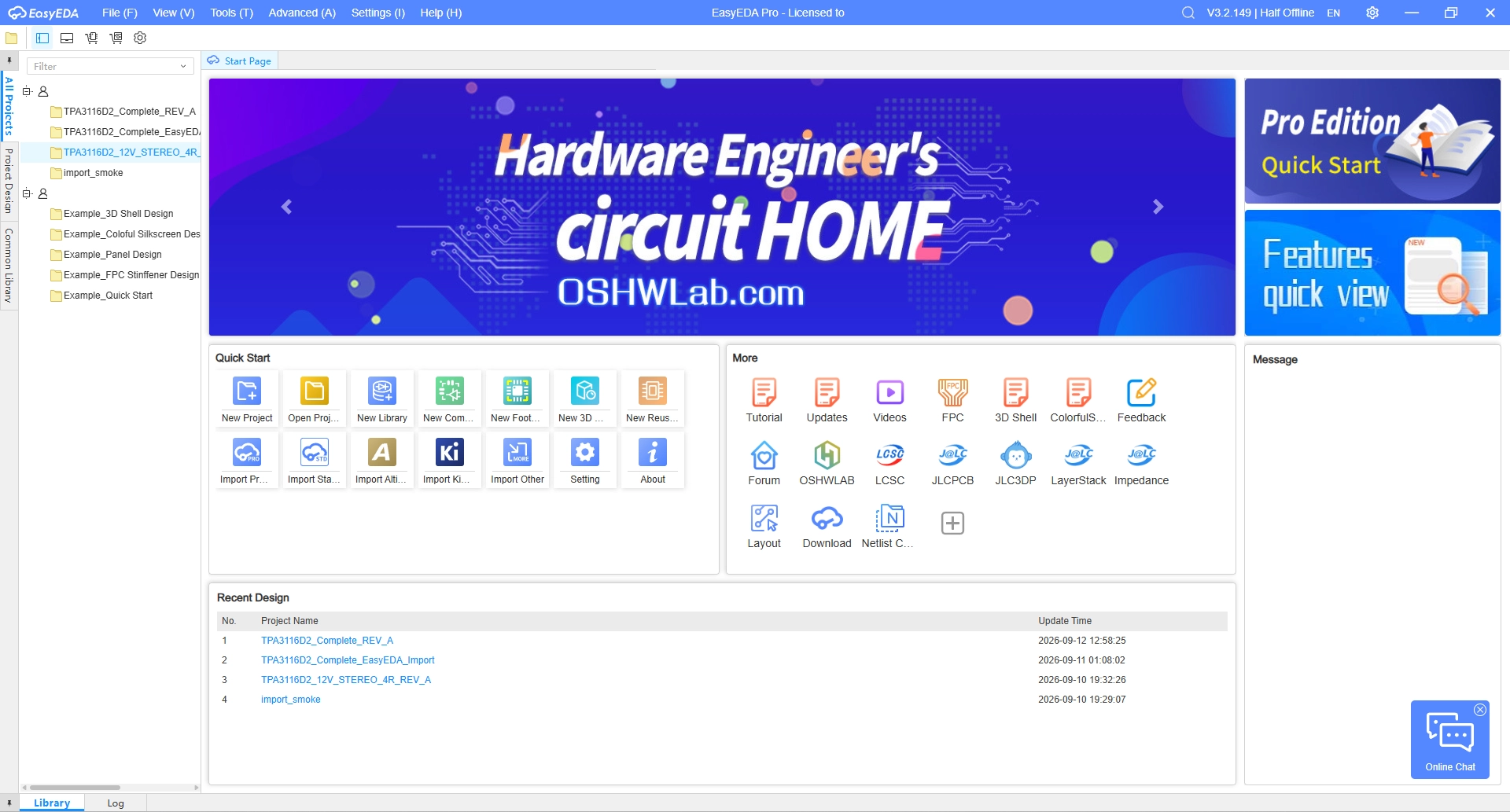
This was one continuous project with repeated corrections, not a set of independent benchmark runs. The result is therefore best read as a case study rather than a score.
- GPT-6 Astra: Read the brief and the references, wrote & build scripts, planned placement, and reviewed each failure before correcting it.
- EasyEDA Pro 3.2.149: Held the editable native schematic, PCB, and embedded libraries, and ran the final native DRC.
- KiCad 10.0.4: Carried the routed manufacturing master, filled the copper zones, and exported the fabrication files.
- Freerouting 2.0.1: Routed the remaining low-current connections once the critical copper had been defined and locked.
The routed master board was first built in KiCad and then imported into EasyEDA. This workflow matters because the imported board structure affects how the ground copper is handled in EasyEDA later. The board construction process, including the scripted build and the issues encountered with the KiCad Python API, is covered in our companion guide, GPT-6 Astra PCB Design in KiCad.
This workflow also requires more than a standard chat interface. The test environment needs access to local files, application control, and locally installed EDA tools, so the tool setup itself is part of the methodology. For comparison, our Flux.ai PCB design walkthrough uses a different tool environment and workflow.
GPT-6 Astra PCB Design in EasyEDA Pro: A Real Test
Before You Start
- A desktop agent environment with file access and application control. A normal chat window cannot drive EasyEDA Pro from a prompt alone.
- EasyEDA Pro is installed and open, plus any routing and export tools you intend to use.
- One project folder holding the datasheet and any reference circuits.
10-step quick workflow
- Collect the reference files into a single project folder and point GPT-6 Astra to that folder.
- Provide the full electrical brief in a single message: supply voltage, channel count, load impedance, component technology, and size limit. A missing load impedance prevents the run from starting.
- Ask that the supplied reference be checked against the current datasheet revision rather than copied, because reference images and older datasheets contain errors.
- Have the schematic built in EasyEDA Pro, then verified pin by pin against the circuit specification, including any intentional no-connect.
- Verify footprints before layout: pin 1 position, pad numbering, polarity, rotation, and an orderable part behind each one.
- Set the design rules to the values you will actually order against, then ask for placement inside a fixed board outline.
- Route the critical copper first, covering supply, bootstrap, and switching outputs, and lock that geometry before any autorouter runs.
- Give every footprint a unique name and identifier before importing, because shared library names merge in the device cache and quietly swap pad orientations.
- Import with File > Import > EasyEDA(Standard), review the schematic-to-PCB changes before applying them, then save and run the native DRC.
- Export the release and check it against your manufacturer's capabilities. A clean DRC reports only the rules you enabled, so it is not a manufacturability check.
Note
The rest of this article covers each step in detail, including the import that logged 50 association mismatches and the fix that cleared it.
Checking the Reference Design Against the TPA3116D2 Datasheet
The supplied reference was treated as something to be verified rather than simply copied. A comparison with the current datasheet identified two circuit details that needed correction, plus one package-related issue.
The first step was to correct three issues:
- Input coupling: The reference uses 1 nF, while this board uses four matched 2.2 µF capacitors on both inputs and their references.
- Bootstrap pairing: Taken from TI datasheet revision G, because the supplied copy predates the correction.
- Package: TPA3116D2DADR in the DAD0032A outline, which puts the exposed thermal pad on top.
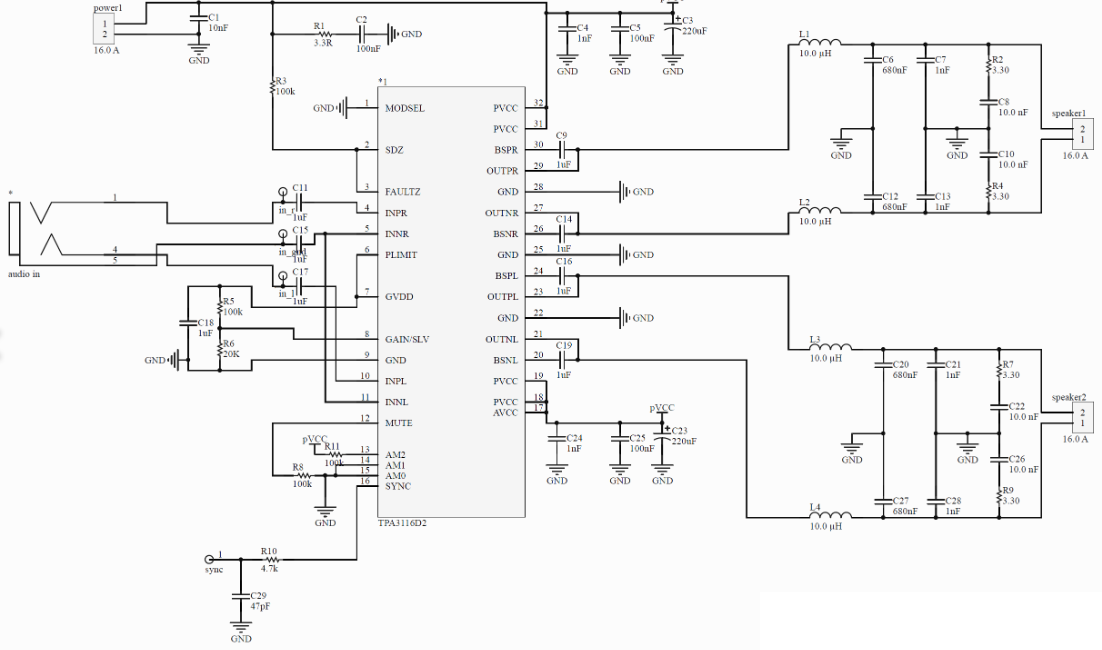
Figure: The supplied TPA3116D2 reference schematic, drawn with 1 nF input coupling capacitors.
Building a TPA3116D2 Schematic with GPT-6 Astra in EasyEDA Pro
The schematic was drawn during this task rather than imported from the reference. It splits the amplifier into seven blocks and ties every symbol pin to a named net. The PCB can then be checked against the same specification.
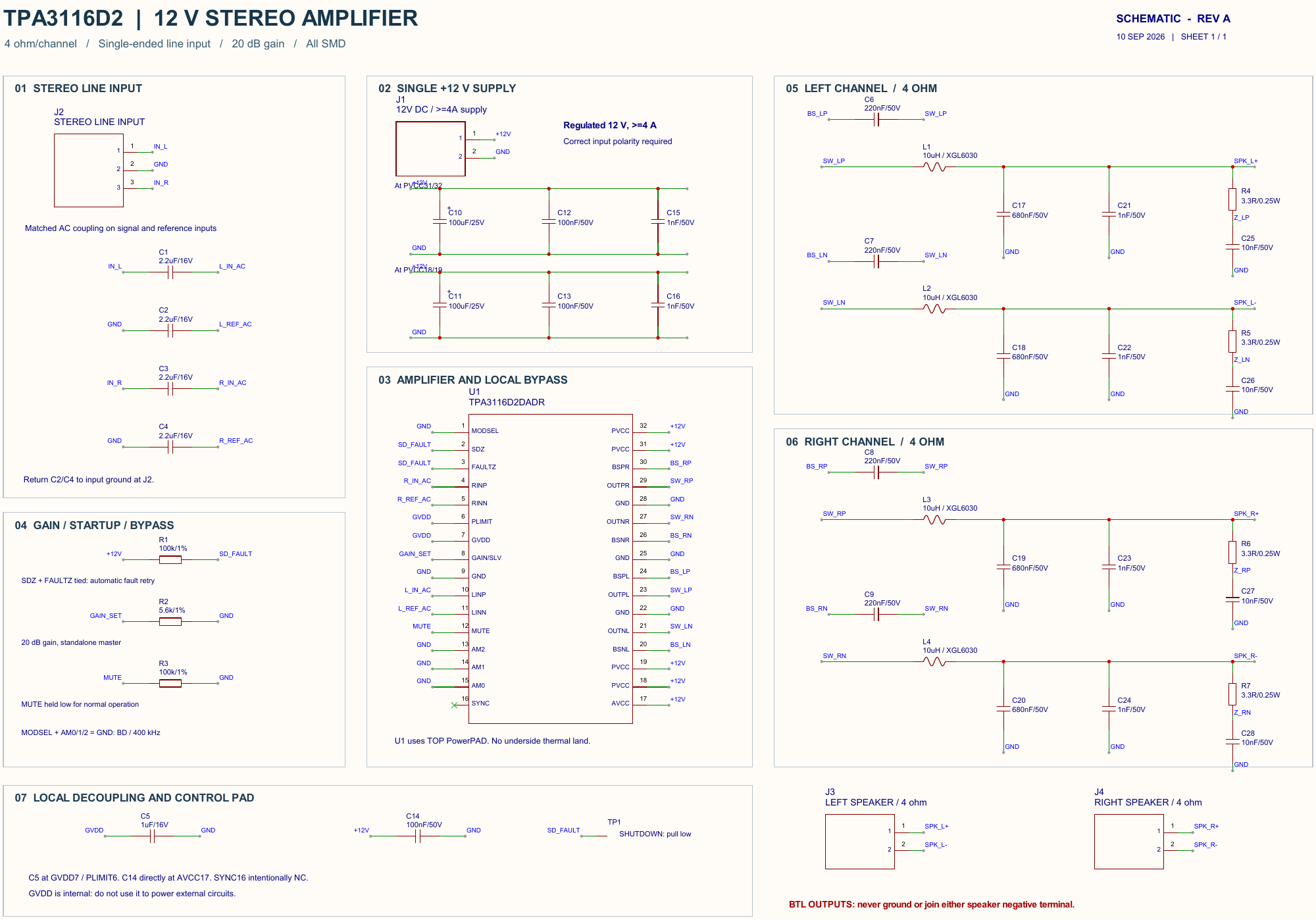
Figure: The completed schematic groups the stereo inputs, supply, amplifier, control circuit, and four output-filter legs.
Input, Gain, and Control
- Four 2.2 µF capacitors couple both signal inputs and their ground references, while the two reference capacitors return to the input ground near J2. R2 sets the master gain at 20 dB through a 5.6 kΩ strap.
- SDZ and FAULTZ are tied together and pulled to +12 V through 100 kΩ, because that is the automatic fault-recovery arrangement TI describes. Pulling the shared net low through TP1 shuts the amplifier down.
- MUTE is held low for normal operation, while PLIMIT is tied to GVDD. SYNC pin 16 is intentionally unconnected and carries a no-connect flag, so a later check can confirm that no wire reached it.
Supply Bypass and Output Filters
The amplifier uses BD modulation at 400 kHz, selected by grounding the MODSEL and AM pins. From there, the supply and output-stage components fall into four main groups:
- Bootstrap: Four 220 nF capacitors, each running from one bootstrap pin to its own switching output.
- Bulk bypass: Two 100 µF 25 V low-ESR hybrid capacitors, one above and one below U1.
- Local bypass: 100 nF and 1 nF ceramics at each PVCC end, a separate 100 nF at AVCC pin 17, and 1 µF on the internal GVDD rail.
- Output filter: 10 µH into 680 nF on each of the four legs, followed by a 1 nF bypass and a 3.3 Ω plus 10 nF damping branch.
These values were chosen specifically for this board, supply voltage, and load. They are not a universal Class-D design recipe. Change the supply, speaker impedance, or switching frequency, and the appropriate component values will change accordingly.
The schematic review also went beyond simply counting symbols, because a symbol count says little about whether the circuit is actually wired correctly. The connections were reconstructed from pin positions, wire traces, and net labels, and then checked against the intended circuit specification.
That established the baseline for the rest of the design: 45 component instances, 120 pins, and 28 nets.
The 45 instances include the wire pads and test pad, so they should not be confused with the 40 physical parts that are actually purchased and assembled on the board.
Verifying PCB Footprints Before Layout
Correct wiring establishes nothing about the copper, because the netlist never sees a pad. Pad numbering, package dimensions, polarity, and rotation all had to stay correct as those symbols became PCB components.
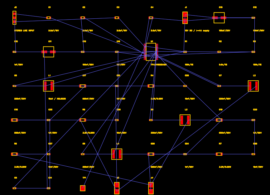
The verification list covered:
- U1 pin 1 position and all 32 pad numbers.
- Positive and negative pads on the polarized bulk capacitors C10 and C11.
- Pad order after rotating the input, control, and output components.
- Surface-only wire pads with no drilled hole and no paste aperture.
- Matching symbol, device, and footprint associations across all 45 instances.
Each footprint should also correspond to a real, orderable component. Verifying the package specification and component availability in the JLCPCB Parts Library early can help ensure the footprint matches a component available for assembly and avoid unnecessary footprint changes later.
Once your footprints and component choices are verified, move from PCB design to assembly with JLCPCB.
Note
The first EasyEDA project was only a footprint staging board, not a finished PCB. Simply opening a project in an EDA tool does not prove the board is complete.
PCB Placement and Routing in a 44 × 34 mm Board
Placement set the signal flow before routing began, so the copper had a direction to follow. Inputs and controls stay on the left, U1 sits in the center, and the inductors and speaker pads occupy the right.
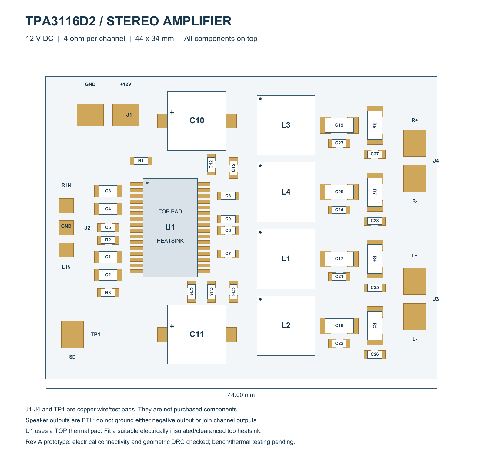
Figure: The assembly map shows input pads on the left, U1 in the center, four inductors on the right, and the reserved top heatsink area.
Signal Flow Across the Board
The inductor order follows the amplifier output pin order, which keeps the switching routes from crossing. The bulk capacitors sit above and below U1, while the local ceramics cluster around their supply pin groups.
The analog inputs stay on the quiet left side, away from the switching output area. That separation matters more when the board is compact, because the switching nodes and the input pins end up millimeters apart.
Placement had to balance several competing requirements:
- Keep the bootstrap and supply-bypass connections short.
- Give the four output paths room to reach their inductors.
- Preserve a usable ground return across the whole board.
- Leave clearance for the top heatsink and the two polarized capacitors.
- Keep the external wire pads reachable at the board edges.
Trace Widths for Power and Signal Routing
The board uses 0.25 mm signal traces, 0.35 mm switching escapes near U1, about 1 mm output traces, and a 2 mm supply trunk. These widths suit this board and its 1 oz copper; they are not universal current limits.
Traces were widened wherever pin spacing allowed. The supply route could also pass under U1 because this package has no exposed thermal pad. The board has 51 plated holes, all used as vias.
There are no mounting holes, keeping the design fully SMD and leaving mechanical mounting to the enclosure. Once the board outline was stable, a quick two-layer FR-4 quote made it easy to check the cost impact of board size before finalizing the layout.
Why Did the First EasyEDA Pro Import Fail?
The first complete import opened normally and looked correct, but the library links were inconsistent. A separate native check reported 50 association mismatches, even though all 120 PCB pad nets were counted correctly.
What the First Native Check Reported
Of the 50 warnings, 20 were footprint mismatches, and 30 were schematic-to-PCB mismatches, all involving repeated component types.
The cause was a shared library name: every 0603 capacitor used C0603, so EasyEDA Pro merged footprints that should have remained separate. Synchronization reduced the warnings from 50 to 20, but did not fully fix them. The key point is that pad net names can remain correct even when the physical footprint association is wrong. That is why all 120 pad nets checked out, while the imported board still had hidden problems.
Fixing the Footprint Association Mismatch
The fix was to give each imported footprint a unique name and ID while keeping it linked to the schematic. For example, C12 became C0603_C12 and R4 became R1206_R4.
After rebuilding and reimporting the schematic-PCB pair, the native check returned 45 parts, 120 pins, 28 nets, and zero errors.
| Import stage | Errors logged by the native check | What changed |
|---|---|---|
| First complete import | 50 association mismatches | Shared footprint names merged in the device cache |
| After synchronizing in EasyEDA Pro | 20 device-to-instance mismatches | Schematic-to-PCB pairs resolved, cache entries did not |
| After the unique-name rebuild | 0 | Every footprint is given a unique name and identifier |
How to Import an EasyEDA (Standard) Project into EasyEDA Pro
The import itself is simple. What matters is the order of the checks before and after it.
- Open File > Import > EasyEDA(Standard).
- Select the ZIP holding both the schematic JSON and the PCB JSON.
- Choose Import Document and Use source file style.
- Keep automatic footprint association enabled and automatic 3D-model association disabled for this import.
- Create the project, open its PCB, and review the schematic-to-PCB changes before applying them.
- Save the synchronized project and run DRC again.
The final synchronization updated names and channel data without moving any verified pads. It also cleared the generated net name from the unused SYNC pad. Solder-mask expansion was set to 0.05 mm per pad edge. Paste was disabled on the wire and test pads, so the stencil applies solder only to fitted SMD components.
What the Native EasyEDA Pro Checks Reported
The final checks compared the saved schematic and PCB data directly, covering connections, pads, traces, vias, and ground regions before running the native DRC.
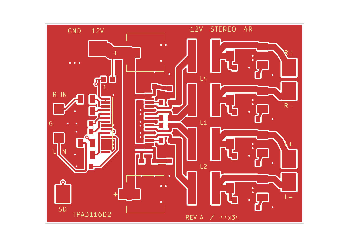
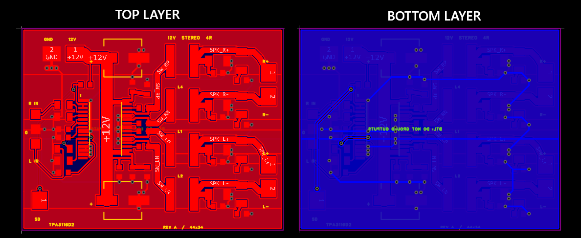
Figure: TPA3116D2 audio amplifier PCB top copper layout showing local ground clearances and four filtered output paths
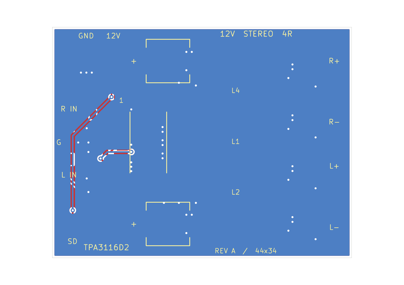
Figure: TPA3116D2 audio amplifier PCB bottom layer, staying almost entirely ground copper with short routes and vias on the quiet input side
The Saved Design Checks
| Check | Result | What it establishes |
|---|---|---|
| KiCad 10.0.4 DRC | 0 violations, 0 unconnected items | Compliance with the enabled board checks |
| EasyEDA Pro DRC | All (0) | No errors in the final native check |
| Native circuit mapping | 45 instances, 120 pins and pads, 28 nets | Schematic and PCB assignments agree |
| Native geometry | 120 pads, 51 vias, 252 copper segments | Matches the exported geometry |
| Ground regions | 28 imported regions | Contours and net assignments checked |
| Outline | 44 × 34 mm | Confirmed in the exported outline artwork |
| Hardware and factory tests | Not performed | No physical performance conclusion |
One important change was documented: EasyEDA dropped a ground segment shorter than 3 µm because its endpoints already overlapped the same-net copper. Connectivity and DRC still passed.
The ground copper was imported as fixed filled regions. If components move, those clearances will not update automatically.
Two options remain:
- Refill the KiCad master and reimport.
- Replace the fixed regions with native EasyEDA copper areas and rerun DRC.
What the Final Release Contains
- TPA3116D2_COMPLETE_REV_A.eprj2:The native EasyEDA Pro schematic, board, and embedded libraries.
- TPA3116D2_Gerbers_44x34mm.zip: Copper, mask, silkscreen, paste, outline, and drill files from the checked master.
- PCB_BOM.csv and PCB_PickAndPlace.csv: Component requirements and placement coordinates for the 40 fitted parts.
- PCB_Assembly_Top.pdf and the schematic PDF: Assembly and circuit references.
- The KiCad board, project settings, and local footprint library: an editable master with refillable ground zones.
- Verification reports and a release manifest: The recorded checks, file sizes, and file hashes.
Why a Clean DRC Is Not a Manufacturability Check
DRC only confirms that the layout complies with the rules set by the design tool. It does not prove that a specific factory can manufacture the board. No DFM upload, factory review, or order was completed in this project, so manufacturability remains a next-step check.
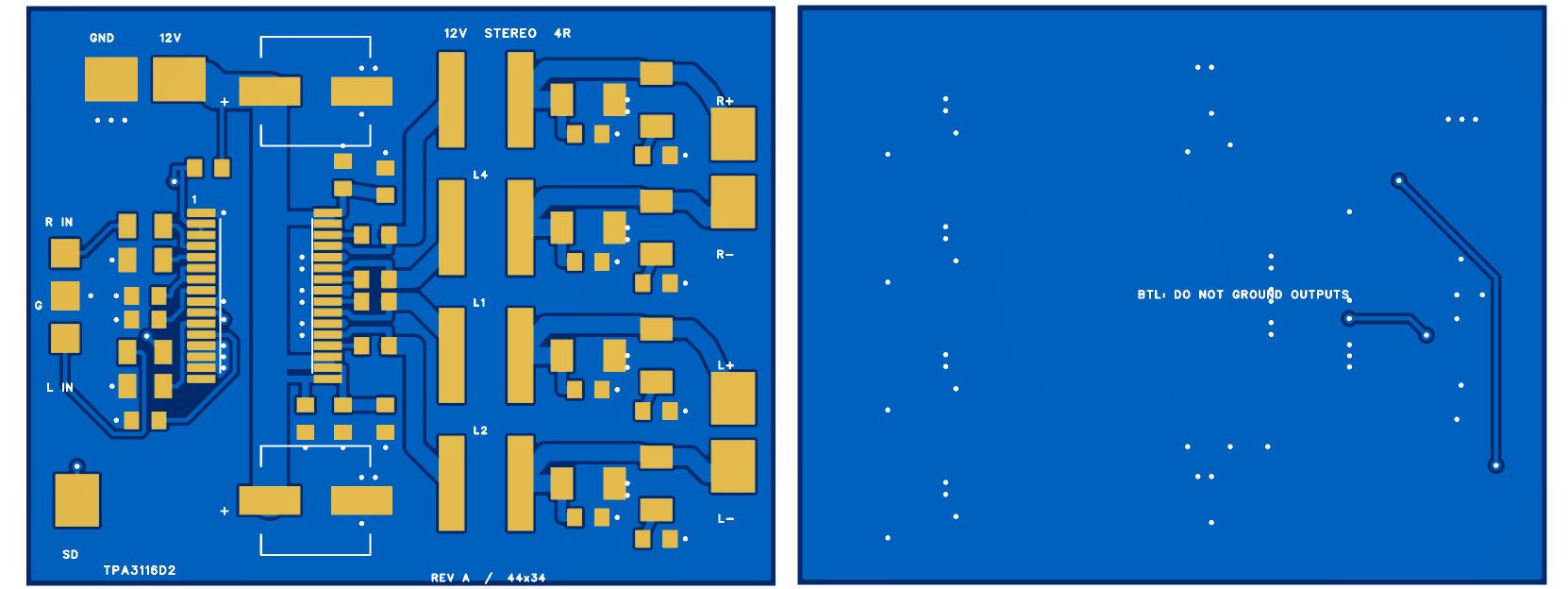
Figure: Side-by-side render of TPA3116D2 audio amplifier PCB top and bottom layers, showing component routing and the bottom ground plane
What to Check Before Manufacturing
- Compare the release against the PCB capabilities and assembly capabilities you intend to order.
- Review layer assignment, outline, drills, mask, paste, copper weight, and panel handling.
- Run the exported files through a factory-oriented analysis, such as the free DFM tool.
- Confirm orderable part numbers, MLCC voltage ratings, and capacitor polarity against the BOM and the assembly drawing.
- Fit a suitable top heatsink with electrical clearance from the IC leads, then power up from a current-limited 12 V bench supply.
Conclusion
GPT-6 Astra turned a four-line brief into an editable EasyEDA Pro project, a routed PCB, and a checked release package. The more important result, however, was finding that a board can open normally and still contain 50 broken library associations. That is why the saved schematic, PCB data, connectivity, and DRC results matter more than a successful import message.
The 2 × 50 W headline rating of the TPA3116D2 should also not be treated as the output power of this board. At a 12 V supply and a 4 Ω load, the real output depends on the available supply current, cooling, and the acceptable distortion level. Those limits were not measured in this project.
The design is therefore electrically checked, but not yet factory-verified. The next step is a proper DFM review against the manufacturer's fabrication and assembly limits before the board is released for production.
FAQs about GPT-6 Astra and EasyEDA Pro
Q: Can GPT-6 Astra Design a PCB in EasyEDA Pro?
In this project, a complete schematic and a routed 44 × 34 mm board were produced inside a native EasyEDA Pro install. The run required file access, local EDA tools, and repeated checks and corrections, so a chat window will not reproduce it.
Q: Does a Zero-Error DRC Mean the Amplifier Works?
No. A DRC result reports the enabled design rule checks on one revision of the layout. It establishes nothing about sound quality, switching behavior, heating, or emissions, all of which need an assembled prototype and a test setup.
Q: Why Did the EasyEDA Import Log 50 Mismatches?
Every repeated component type arrived with the same footprint name, such as C0603, so EasyEDA Pro's device cache merged footprints that were meant to stay separate. Unique footprint names and identifiers cleared all 50 messages.
Q: Can the Imported Board Be Edited in EasyEDA Pro?
Yes, for components, tracks, vias, and schematic data. The ground copper is imported as fixed-filled regions. Moving a part does not rebuild the clearance opening around it, so those regions need to be regenerated before the next DRC run.
Q: Does All-SMD Mean the Board Has No Holes?
No. SMD describes how the components attach, and every fitted part here mounts on the surface. The board still has 51 plated 0.30 mm vias connecting its two copper layers, and it has no through-hole components.
Popular Articles
• AI PCB Design: From Prompt to PCB with EasyEDA Pro
• AI Tools for PCB Design: Which Tool Fits Your Workflow Stage?
• GPT-6 Astra PCB Design in KiCad: From Brief to Verified Native Project
• GPT-6 Astra PCB Design in EasyEDA Pro: What Worked, What Failed, and What We Learned
• How to Design Your Own Keyboard PCB: From Layout to Firmware
Keep Learning
AI Tools for PCB Design: Which Tool Fits Your Workflow Stage?
AI tools can now assist with PCB architecture, schematic generation, component selection, placement, routing, and design verification. However, different tools target different stages of the PCB workflow. This guide compares AI tools for PCB design based on what they actually do, what inputs they require, and where they fit within a real engineering workflow. In this guide, you will learn: The 6 types of AI PCB tools and the input each one needs What AI PCB design tools do, compared stage by stage How......
Free Online Circuit Simulator for Electronics Engineers
Key Takeaways Simulate First: Free circuit simulators prevent fried components and cut PCB re-spins. Fix AC Sweep: Enter pure numbers for points per decade, not time units. Use SMD Parts: Swap ideal models for standard SMD resistors and SOT-23 transistors. Control Parasitics: Board trace capacitance and via inductance alter high-frequency signals. Verify Before Order: Pair SPICE simulation with DFM checks to ensure board success. If all electronic engineers had a dollar for each burnt-out resistor or ......
Mastering PCB Design Rules: A Comprehensive Guide for Optimal Results
Key Takeaways Follow core PCB design rules for reliable electrical and mechanical performance. Optimize trace width, spacing, impedance, and vias for signal integrity and manufacturability. Apply DFM and DRC early to identify potential manufacturing and layout issues. Consider thermal management, grounding, and testing during the PCB design stage. Align design rules with your PCB manufacturer’s capabilities to improve production reliability and reduce redesigns. PCB design rules are essential guidelin......
KiCad MCP: How to Design a PCB with Claude Code [Step-by-Step]
Key Takeaways Claude can design PCBs in KiCad: By connecting Claude to KiCad through an MCP server, you can use AI to create and modify PCB designs. In this project, Claude helped turn a 5 A XL4015 buck converter netlist into a two-layer, 63 × 33 mm PCB layout with zero ERC violations and zero DRC errors after minor initial fixes. Set up Claude securely: Use a KiCad MCP server that starts in read-only mode. Review the server code before installing it, connect through stdio, and allow editing only in a......
Claude Code PCB Design: Can It Build a Real Board in EasyEDA Pro?
Key Takeaways Claude Code PCB design: Using Claude Opus 5.5 and EasyEDA Pro 3.2.149, I converted a 47-component, three-page schematic from a PDF into a fully routed, two-layer PCB with zero DRC errors. EasyEDA Pro integration: The EasyEDA API skill connects Claude Code to EasyEDA Pro through a local bridge server and the Run API Gateway extension. This allows Claude to control the editor via JavaScript, with a 30-second timeout per API call. Design verification: A successful API response doesn't alway......
How to Design a PCB with Flux.ai (Step-by-Step Guide)
Key Takeaways This step-by-step Flux PCB design tutorial demonstrates the complete workflow by creating a compact 15 × 15 mm USB 2.0 hub, refining the layout, routing high-speed differential traces, and preparing manufacturing files for JLCPCB PCB fabrication and assembly. We are all hearing news; new AI models are being released every month. And it has finally reached the schematic editor. Flux.ai is a browser-based AI PCB design tool with a built-in AI agent that behaves like a junior hardware engin......