GPT-6 Astra PCB Design in KiCad: From Brief to Verified Native Project
19 min
- 10-Step Workflow: GPT-6 Astra PCB Design in KiCad
- What OpenAI Actually Showed GPT-6 Astra Doing in KiCad
- What GPT-6 Astra Did in the KiCad PCB Project
- Building the Native Schematic in KiCad 10.0.4
- Managing Footprints, Libraries, and Component Links in KiCad
- What GPT-6 Astra's KiCad Verification Actually Proves
- PCB Placement, Copper Zones, and DRC in KiCad
- Exporting KiCad Gerber Files and Assembly Data
- Why a Clean KiCad DRC Is Not a Manufacturability Check
- Conclusion
- FAQs about GPT-6 Astra and KiCad

Key Takeaways
- What OpenAI published: The launch page features a 15-second condensed clip of GPT-6 Astra performing PCB layout in KiCad.
- What the model did: It turned a four-line brief into a 44 × 34 mm, two-layer PCB, covering the circuit, footprints, component placement, routing, and a native two-sheet schematic.
- Where the work went: Placement and routing were only part of the work. Two linked schematic sheets, project-local libraries, and UUID-based links between 45 components and their footprints were critical to keeping the project consistent.
- The useful finding: KiCad reported 46 schematic-parity issues. They were cleared by correcting component fields and the no-connect representation, not by adding rule exclusions.
- What zero violations mean: KiCad 10.0.4 reported 0 ERC and 0 DRC violations under the configured rules. Five DRC categories and four ERC categories were ignored.
A PCB generated by GPT-6 Astra can look simple at first, but building a clean native KiCad project takes more than producing a routed board. The schematic, libraries, footprints, and component links must all agree.
In this project, GPT-6 Astra built and checked a TPA3116D2 stereo amplifier in KiCad, focusing on a consistent native project rather than a PCB that only looks correct.
In this guide, you will learn:
- What OpenAI actually says about GPT-6 Astra and KiCad
- How the board went from a four-line brief to a routed two-layer PCB
- How 46 schematic-parity issues were resolved without adding exclusions
- What zero ERC and DRC violations do and do not mean
10-Step Workflow: GPT-6 Astra PCB Design in KiCad
The workflow has ten stages. Use this overview before diving into the details.
Before You Start
- A desktop agent environment with file access and application control, since a chat-only interface cannot directly operate KiCad.
- KiCad 10.0 or newer, plus a local autorouter if you intend to use one.
- One project folder containing the datasheet and any reference designs.
The Ten Short Steps
- Collect the datasheet and reference files in a single project folder, then give GPT-6 Astra access to it.
- Provide the full brief in a single message: supply voltage, channel count, load impedance, component technology, and size limit.
- Verify the reference design against the current datasheet revision instead of copying it directly.
- Have the schematic built as native KiCad objects, split across a main sheet and a second sheet.
- Verify every footprint before layout, including pin 1, pad numbering, polarity, orientation, and orderability where applicable.
- Set the design rules to the values you will order against, then place components within the fixed board outline.
- Define and lock the critical supply, bootstrap, and switching copper first.
- Let the autorouter finish the low-current nets, then refill the zones and confirm the locked copper survived.
- Package the required libraries with the project and verify that every schematic component is linked to the correct PCB footprint.
- Run ERC, DRC, unconnected items, and parity together, then export the Gerbers, drill files, BOM, and placement file.
Note
A clean ERC/DRC check only confirms compliance with the rules you enabled. It is a design milestone, not manufacturing approval; the final design must still be checked against the fabricator's manufacturing capabilities.
What OpenAI Actually Showed GPT-6 Astra Doing in KiCad
OpenAI published a condensed video of the model performing PCB layout in KiCad. Nothing on the page goes further, however, which is why the exact wording matters.
The caption is specific about its own scope. It reads: "This is a 15-second condensed playback of GPT-6 Astra performing printed circuit board (PCB) layout in KiCad, turning an electronic schematic into a manufacturable PCB by placing components and routing copper connections."
| Claim | Where it comes from | Status |
|---|---|---|
| Astra performing PCB layout in KiCad | OpenAI launch page caption, 3 September 2026 | Primary source, quoted verbatim |
| OSWorld 2.0 of 72.6% against 65.7% for GPT-5.6 Sol | OpenAI launch page, v2026.08.08 offline set, partial score | Primary source, on computer use |
| A "2 min 54 sec" label beside the PCB figure | OpenAI launch page markup | Primary source, but the panel it labels needs visual confirmation |
| "OpenAI claims Astra can make PCB boards" | Title of a KiCad.info forum thread | Secondary framing, not OpenAI's wording |
| "OpenAI is showcasing KiCad integration" | Title of a Reddit post | Unsupported, since no plugin, API, or partnership has been announced |
| A 69.3% EEBench score proves layout ability | Secondary reporting | Unsupported, because EEBench excludes layout |
Computer Use Skill Is Not a KiCad Integration
Computer use means the model reads the screen and issues mouse and keyboard actions. It therefore acts as a user of KiCad because it lacks its own routing engine and design rule checker.
When copper appears to be routed, KiCad's own tools are doing the geometric work. No KiCad code changed hands, so no relationship between OpenAI and KiCad follows from the demonstration.
What the 15-Second Clip Leaves Out
The caption starts from an existing schematic. Several stages of a real board, therefore, sit outside the frame:
- Schematic capture: Symbol selection, pin types, and net definition all happened before the clip begins.
- Part selection: Nothing in the clip covers choosing a package, a voltage rating, or a supplier.
- Rule resolution: A placed layout still has to survive a design rule check, but the clip ends earlier.
- Project structure: Libraries, schematic-to-board links, and portability stay invisible in a rendered view of copper.
- Manufacturing: Gerber export, drill generation, placement data, and factory review all sit outside it.
What GPT-6 Astra Did in the KiCad PCB Project
I began a new TPA3116D2 stereo amplifier PCB project with an electrical design brief and supplied reference files. The goal was a compact board with a single 12 V supply, stereo line input, two 4-ohm speaker outputs, and SMD components only.
GPT-6 Astra did the design work from that brief onward, and it carried every stage below:
- Circuit development: Astra extracted the circuit from the datasheet and references, then verified the values, packages, and pin assignments before they were connected.
- Footprint verification: It checked pad numbering, polarity, rotation, and land dimensions against the manufacturer's drawings.
- Placement: It arranged the inputs, amplifier, supply bypass, and output filters within a 44 x 34 mm, two-layer outline.
- Routing: It first defined and protected the critical power, bootstrap, and switching connections, then ran local Freerouting to complete the remaining low-current nets.
- Native project and release: It built the two linked schematic sheets, packaged the libraries, ran the checks, and exported the manufacturing files.
KiCad held the routed PCB and refillable ground zones, while the final native project added two linked schematic sheets. A usable release needed more than a board that opened correctly. The schematic, PCB, libraries, and project links all had to stay consistent.
The board has 45 footprint instances and 120 SMD pads, but only 40 fitted components. J1–J4 and TP1 are wire-and-test pads, so they are excluded from the BOM and placement file.
The Prompts Behind the Project
Six recorded prompts carried the whole project. The requirements set the electrical and physical targets, and the follow-ups continued the work and named the final deliverables.
| Stage | Recorded prompt |
|---|---|
| Opening the design application | "Can you use the KiCad open on my computer to make a PCB? Can you access that?" |
| Providing the reference files and requirements | "In the TPA3116D2_PCB/ there are some design files and a reference PCB design. First, make the schematic. My requirements are such that I will use it with a 12V single-supply. I need stereo input and output. You have to use SMD components only for this design. I will keep the PCB as small as possible - when making the PCB." |
| Specifying the speaker load | "4 Ω per channel" |
| Requesting the completed layout | "Do it, complete the PCB design." |
| Requesting the native project and article | "Okay, do it. Give me PCB with native KiCad and blog" |
| Opening the finished PCB | "open the pcb in KiCad" |
Detailed circuit decisions, routing corrections, and verification took place between those prompts.
Building the Native Schematic in KiCad 10.0.4
The circuit reference came from the device datasheet. GPT-6 Astra extracted the required circuit from that reference and rebuilt it as a native KiCad schematic with real symbols, pins, wires, and net labels, rather than as an embedded image.
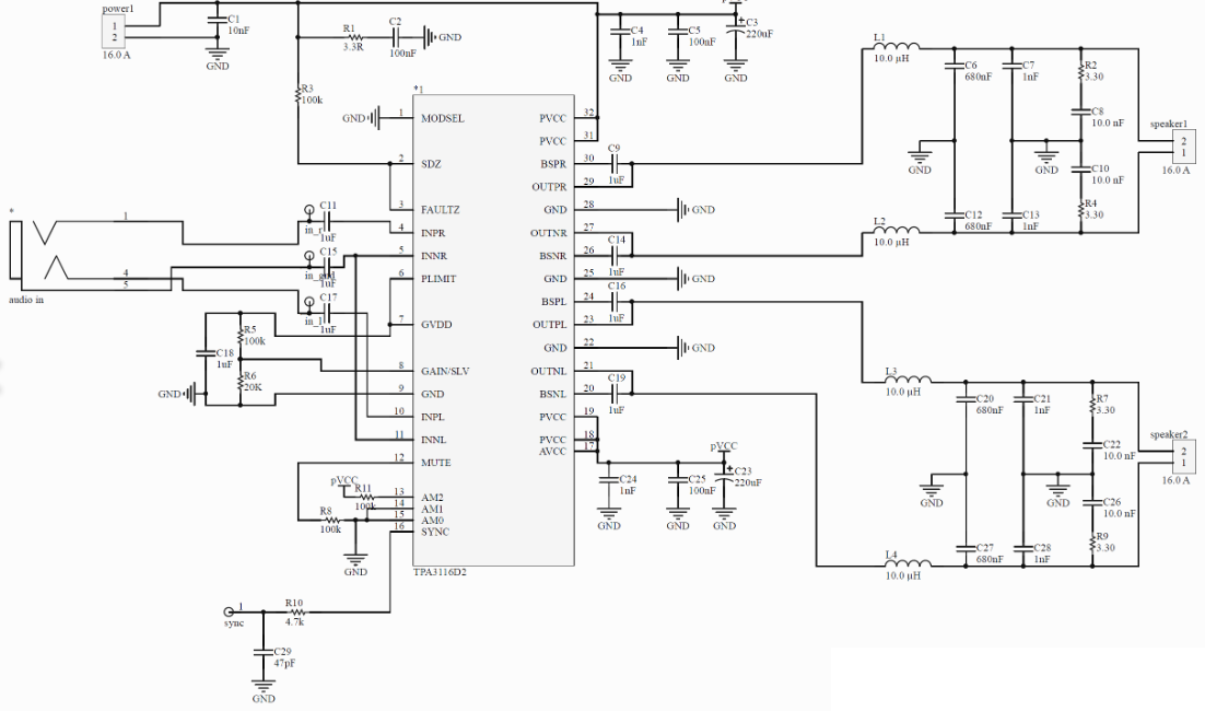
Because the schematic remained fully editable, KiCad could run electrical checks and compare them with the PCB. The datasheet served as the independent reference throughout, since a schematic can appear correct yet still contain an incorrect or missing connection.
Main Sheet: Input, Supply, and Control
The root sheet carries the amplifier, its supply bypass, and its configuration straps. Four 2.2 uF X7R capacitors AC-couple both signal inputs and their ground references, and C2 and C4 return to the input ground near J2.
Supply bypass is split deliberately across three ranges:
- Bulk. Two 100 uF 25 V low-ESR capacitors hold the local charge close to the device.
- Mid-frequency. Each PVCC pair carries its own 100 nF at the supply pins.
- High-frequency. Each PVCC pair also carries 1 nF, and AVCC on pin 17 gets a separate 100 nF because it feeds the analog side.
Three resistors and one pad set the configuration. R2 at 5.6 k selects the 20 dB gain setting, while R1 and R3 at 100 k handle the linked SDZ and FAULTZ pull-up and the MUTE hold.
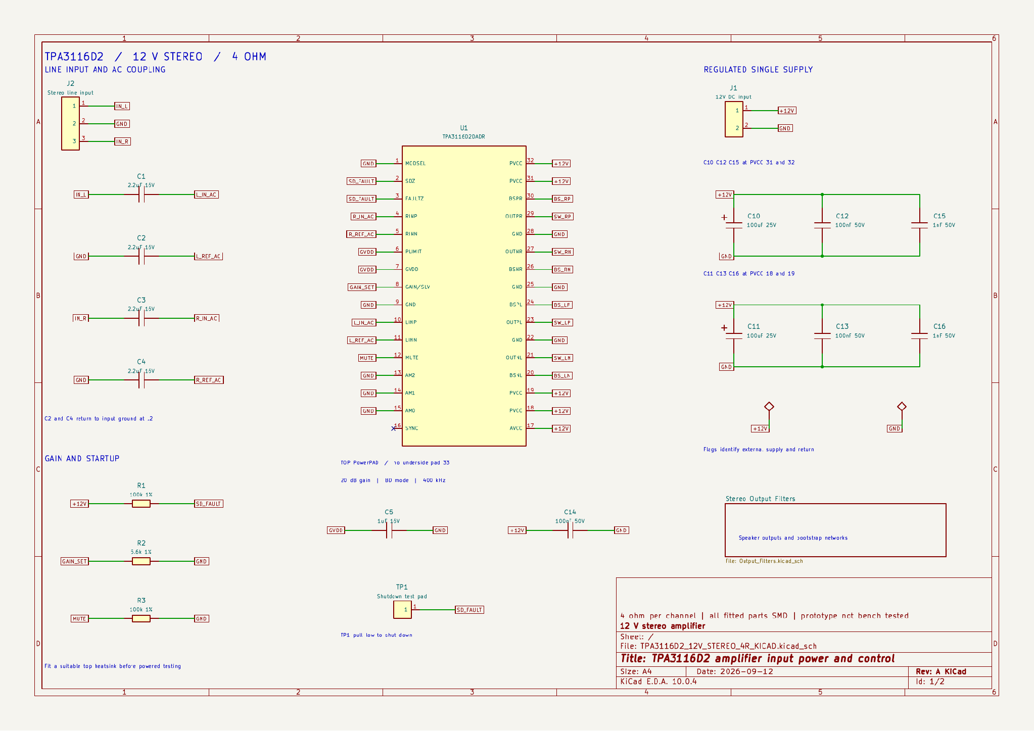
Figure: The root KiCad schematic sheet exported from the native project, carrying the stereo input, U1, supply bypass, and control network.
Second Sheet: Bootstraps, Output Filters, and Speaker Pads
A 2nd sheet named `Output_Filters.kicad_sch` holds the repeated networks. That split keeps both pages legible at publication width.
Each output leg uses a 10 uH inductor, followed by a 680 nF capacitor and a 1 nF bypass. A series 3.3 ohm plus 10 nF branch returns to ground, so the filter is damped rather than left to ring.
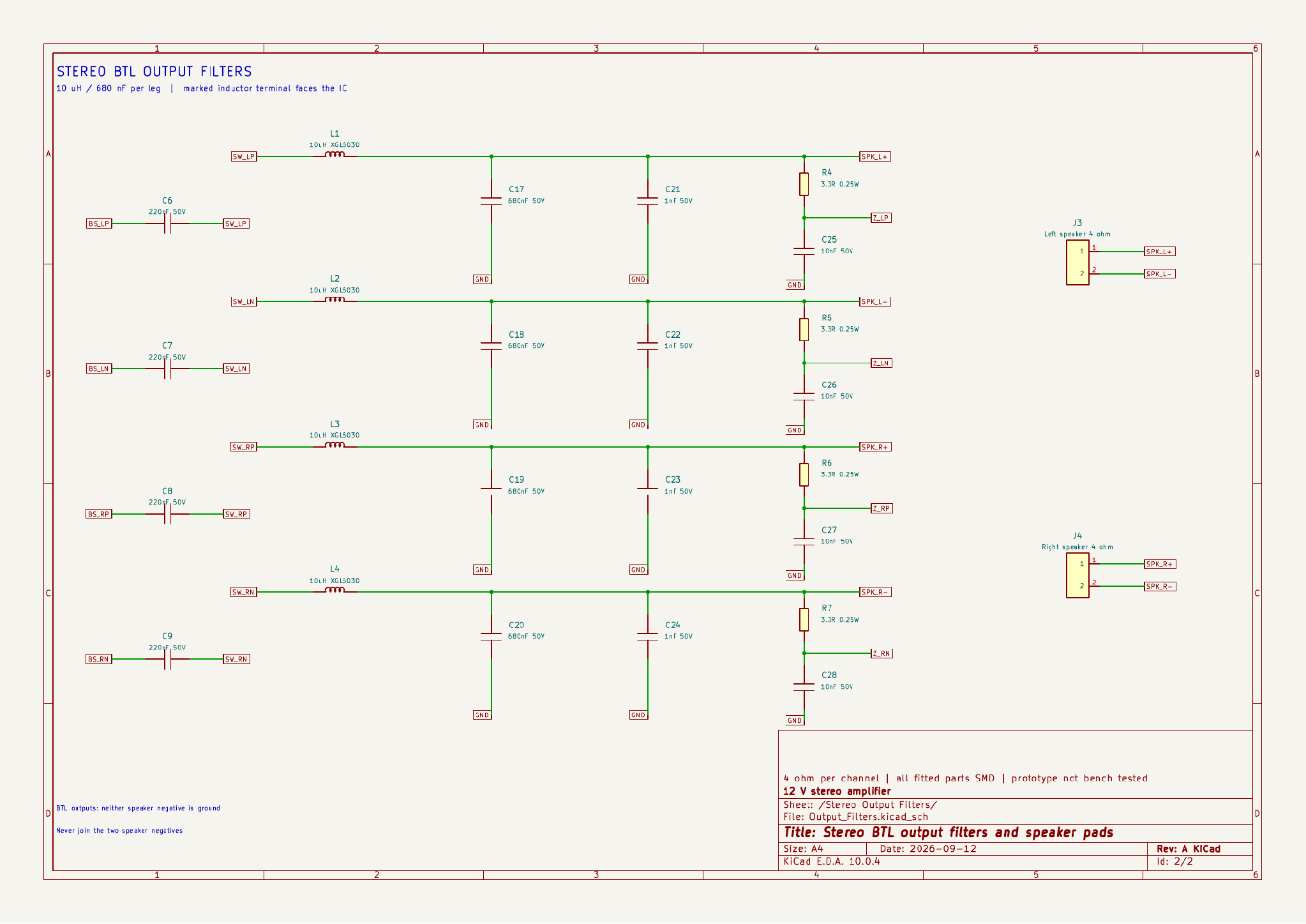
Figure: The Output_Filters child sheet exported from the native project, grouping the bootstrap capacitors, four LC output legs, and speaker pads.
The four 220 nF bootstrap capacitors also sit here. Their pin pairings are worth stating, because a wrong pairing survives a visual review.
The left channel runs BSPL 24 to OUTPL 23 and BSNL 20 to OUTNL 21. The right channel runs BSPR 30 to OUTPR 29 and BSNR 26 to OUTNR 27. Reversing a pair inside one channel is an electrical error, however, not a cosmetic one.
Resolving 46 Schematic Parity Issues Without Adding Exclusions
KiCad’s first parity check found 46 issues, mainly missing Manufacturer and Rating fields, as well as the intentionally unconnected SYNC pin.
These were not routing or clearance errors. The PCB geometry could still be valid while the schematic and component data did not fully match. All 46 issues were fixed in the source data. No new exclusions were added just to make the report pass.
Managing Footprints, Libraries, and Component Links in KiCad
A native project is portable only if its symbols and footprints travel with it. Astra, therefore, packaged the required definitions beside the project rather than resolving them from a personal library.
1. Local Libraries and Project Library Tables
Three files carry the library side of the project. All of them resolve inside the project folder, so nothing in the release depends on the machine that built it.
- `TPA3116_Native.kicad_sym` holds the project symbols with explicit pin electrical types, including power inputs on the GND, AVCC, and PVCC pins.
- `TPA3116_SMD.pretty` holds 45 land patterns, one per footprint instance, matching what the board already uses.
- `sym-lib-table` and `fp-lib-table` resolve both libraries through `${KIPRJMOD}`, so the paths stay relative to the project.
Declaring pin types is what gives the electrical check something to test. An ERC pass means little when every pin is marked passive, and it means more when supply pins are declared as power inputs.
2. Component Links and 3D Model Paths
Two other links connect the schematic to the PCB, even though they are not visible in the copper view:
- Schematic UUID paths link each symbol to its exact footprint.
- 40 project-relative 3D model links keep the component models tied to the project folder.
These links matter when the design is edited. If they remain intact, schematic updates modify the correct PCB component, whereas a broken link can make the tool treat that component as a replacement instead.
3. Testing KiCad Project Portability in a Separate Directory
Astra tested portability rather than assuming it. It copied the native files, both local libraries, and all model files to a separate directory, then reran ERC and DRC with schematic parity there.
That copy returned zero violations, zero unconnected items, and zero parity issues. No absolute path or missing library surfaced, so the release does not depend on the machine that built it.
What GPT-6 Astra's KiCad Verification Actually Proves
One was an electrical agreement between the schematic and the board, and the other was whether the reused layout survived unchanged.
| Check | Result | What it covers |
|---|---|---|
| KiCad ERC | 0 violations | Enabled schematic rules across both sheets |
| KiCad DRC | 0 violations | Configured board constraints, run with a zone refill |
| Unconnected items | 0 | No unfinished required connections reported |
| Schematic parity | 0 issues | Component fields and pad nets agree with the schematic |
| Independent pin and pad comparison | 120 pairs checked | Native netlist against the original circuit specification |
| Geometry comparison | Preserved | Placement, pads, tracks, vias, zone outlines, and board outline |
| Recheck after copying the project | 0 / 0 / 0 / 0 | ERC, DRC, unconnected items, and parity in a separate directory |
The independent check mattered most. Two files can match and still share the same mistake, so all 120 pin-to-pad connections were also compared against the original saved specification.
What the Ignored KiCad DRC and ERC Rules Mean
A zero-violation result only applies to the checks that were enabled.
- DRC ignored five categories: missing courtyards, off-center via endpoints, tuning-profile geometry, footprint filter mismatch, and component-type mismatch.
- ERC ignored four categories: singleton global labels, four-way junctions, SPICE model issues, and footprint filters.
If a check is disabled, it cannot report an error. Those nine ignored categories are therefore part of the result, not minor footnotes.
Why the Checks Ran From the Command Line
Astra ran verification and CAD export using KiCad's command-line tools because its first application launch request timed out. PCB Editor later opened the finished board, and its status area reported the same counts as the saved reports.
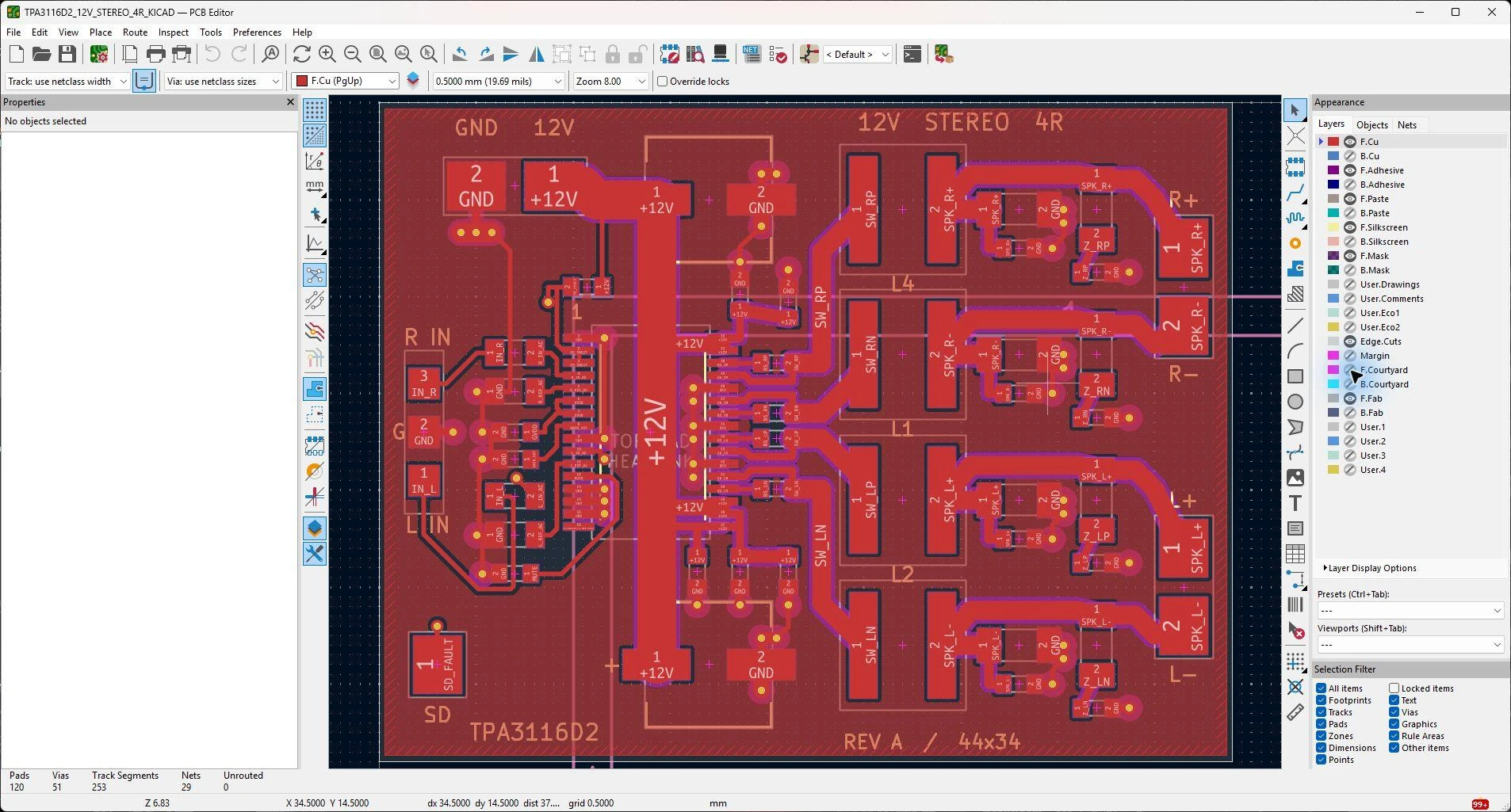
Figure: An actual KiCad PCB Editor screenshot whose status area reads 120 pads, 51 vias, 253 track segments, and 0 unrouted connections.
PCB Placement, Copper Zones, and DRC in KiCad
This KiCad project keeps two editable ground zones, one on each copper layer so that they can be refilled after layout changes.
In the EasyEDA version, the same copper was converted into 28 fixed-filled regions due to the conversion method used. That does not mean EasyEDA lacks native copper areas. That import also reported 50 association mismatches before they were fixed.
What Changes After You Move a Component in KiCad
Three editing tasks behave differently once the zones are refillable rather than fixed. Each one still ends in a fresh set of checks:
- Moving a component: A refillable zone regenerates its clearance opening on the next refill, whereas a fixed region keeps the old opening until someone rebuilds it.
- Changing the schematic: Update PCB from Schematic (normally F8) applies the edit to the linked components, and the change list should be reviewed before it is applied.
- Confirming the revision: Refilling copper does not repair a broken track or a lengthened return path, so ERC, DRC, and parity all need to be rerun.
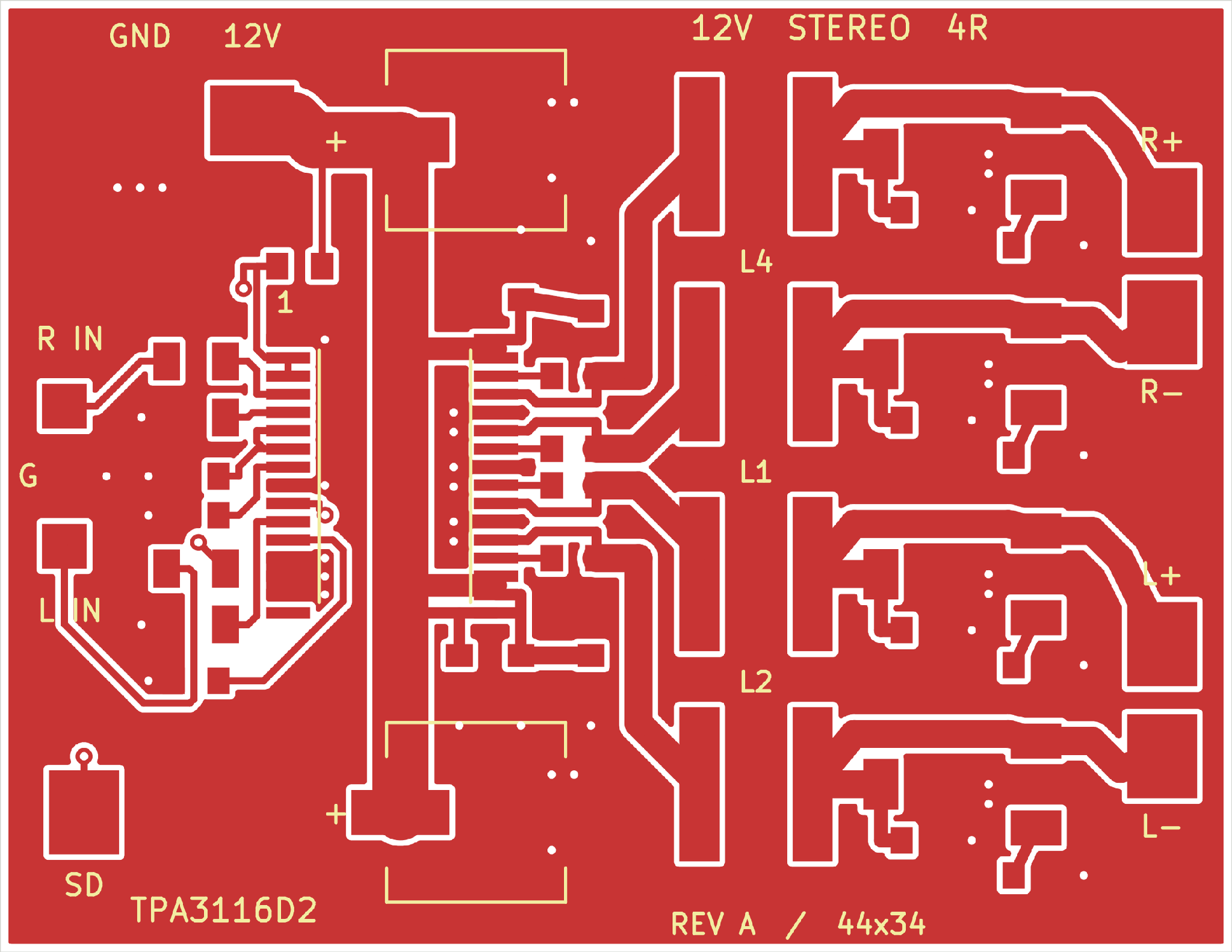
Figure: The KiCad front copper plot exported from the native board, showing the routed front-layer connections and the zone clearance openings.
Use a copy for further edits and keep the checked release as the baseline. KiCad 10 documents the refill, update, and hierarchy tools in its manual.
Exporting KiCad Gerber Files and Assembly Data
Astra exported fabrication data fresh from the checked native board. The artwork, therefore, matches the design that passed the checks rather than any intermediate state.
What the KiCad Manufacturing Export Contains
- Nine artwork layers: Copper, solder mask, and silkscreen for both sides, plus top and bottom paste and the board outline, with the mask subtracted from the silkscreen.
- Two Excellon drill files: Plated and unplated holes are written separately, in millimeters, from the drill-file origin.
- A drill report records 51 plated 0.30 mm holes and 0 unplated holes, so every hole here is an interconnect via.
- Placement and BOM data: The placement file lists the 40 fitted top-side SMD parts, and the native BOM adds manufacturer, MPN, and rating fields.
Coordinates in the placement file are in millimeters, with X to the right and Y up. The board's upper-left corner is at the origin, so Y values are negative, and the rotation convention needs to be confirmed with the assembler.
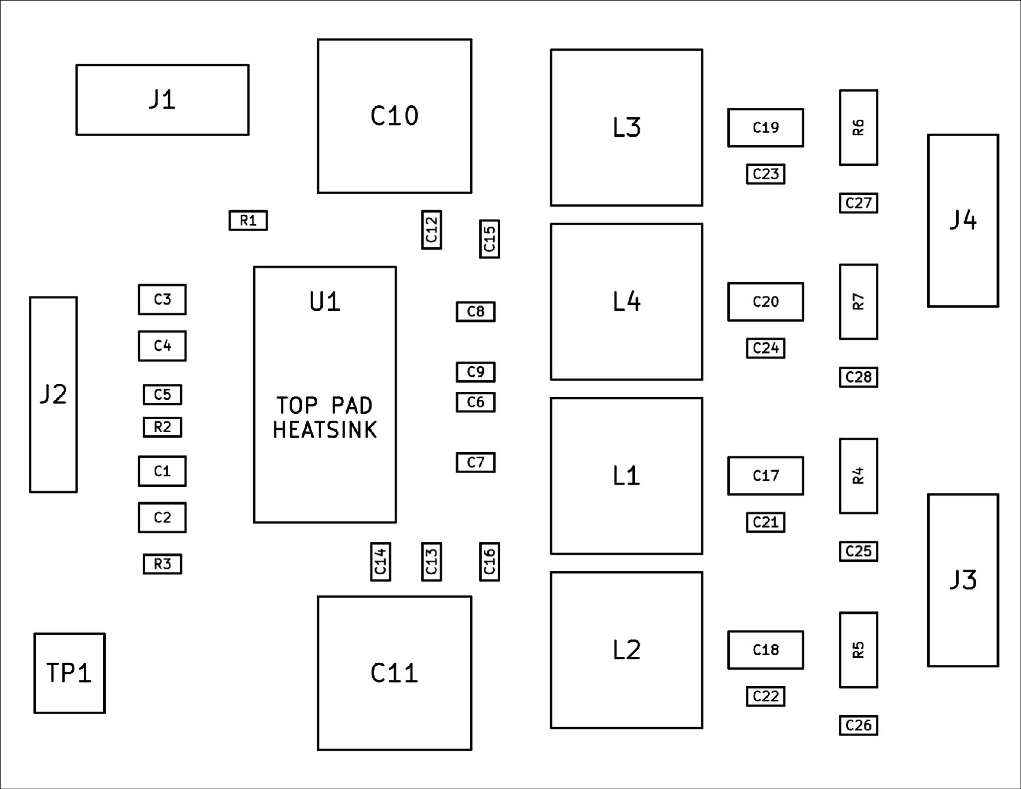
Figure: The KiCad fabrication layer plot exported for assembly, identifying each reference designator and the reserved top heatsink area.
Note
Some BOM entries still use generic or manufacturer part numbers, so the exact orderable parts need to be confirmed before assembly.
This is where a component library can help: the JLCPCB Parts Library lets you check available parts and verify details such as package, dielectric, and voltage rating before placing an assembly order.
Why a Clean KiCad DRC Is Not a Manufacturability Check
DRC checks the rules defined in the design. A manufacturing review checks whether a specific factory can build the board. Neither can be trusted without the right constraints.
Board-Level Checks for Manufacturing Review
- Stackup and copper weight: Track widths assume a nominal 1.6 mm FR-4 with 1 oz copper, so any change in finished weight affects the current and thermal assumptions behind them.
- Annular ring and drill: A 0.30 mm drill in a 0.60 mm via pad leaves a 0.15 mm annular ring. Check that figure against the published PCB capabilities.
- Mask and paste: Solder mask expansion is set to 0.05 mm per pad edge, and the wire and test pads carry no paste openings by design.
Assembly and Qualification Checks
- Assembly feasibility: The tightened C11 courtyard allowance, the clearance between inductor bodies, and the heatsink keep-out need an assembly capability review.
- Thermal provision: A suitable top heatsink or spreader is required, and it is not modeled anywhere in this release.
- Electrical qualification: Capacitor bias and ripple ratings, supply headroom, and wire strain relief stay open on a Rev A prototype.
A DFM analysis and a design verification pass are the next steps, rather than completed ones. No DFM upload, factory review, quotation, or order formed part of this project.
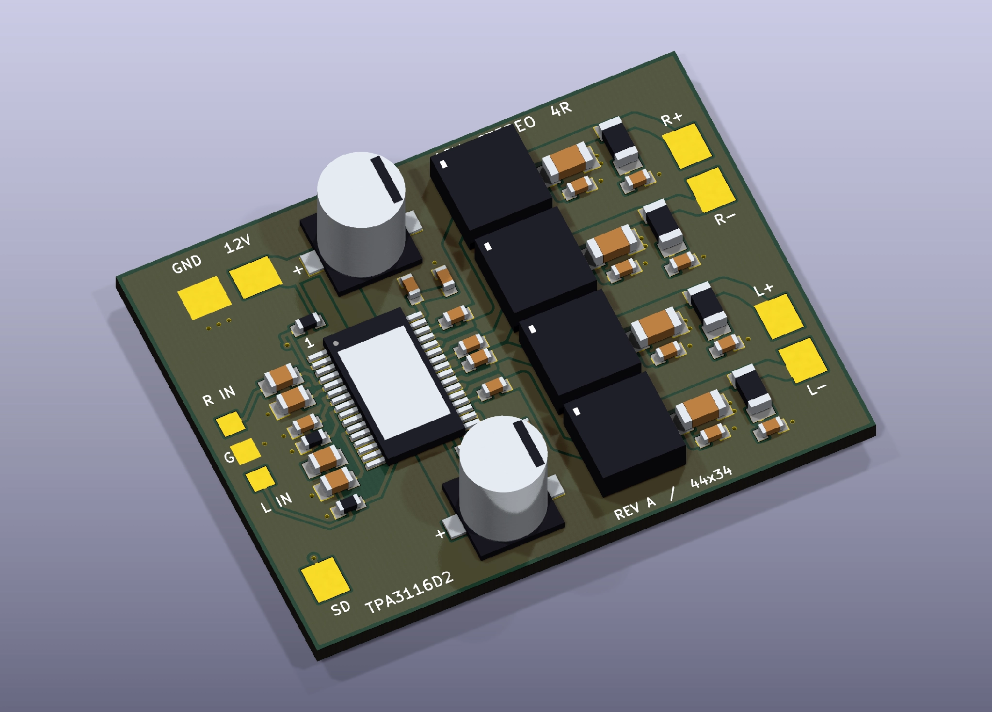
Figure: An approximate KiCad 3D visualization from simplified project-authored models, with no heatsink fitted and no fit check performed.
This board has never been fabricated, assembled, or measured, so its output power, temperature, and electromagnetic behavior remain unverified. The TPA3116D2 datasheet headline 2 x 50 W figure is not a rating for a 12 V board.
Conclusion
This GPT-6 Astra KiCad project shows that a valid board file and a clean native project are not the same thing. The real work was making sure the schematic, component data, footprints, and PCB all agreed. Component selections, such as the Coilcraft inductors and Panasonic capacitors, also need to be checked against the exact parts ordered.
AI tools can speed up schematic capture, layout, and project rebuilding, but they do not remove the need for engineering verification.
Whether the design comes from GPT-6 Astra, Flux.ai, or another AI-assisted EDA workflow, the final checks still belong to the designer. Before ordering, verify the native project, confirm the actual components, and check the design against the fabricator’s manufacturing limits.
FAQs about GPT-6 Astra and KiCad
Q: Did GPT-6 Astra Route This KiCad Board?
No, because the routed 44 x 34 mm layout came from an earlier amplifier task and was reused unchanged. A geometry comparison then confirmed that placement, pads, copper, zone outlines, and the board outline all matched that of the master.
Q: Does GPT-6 Astra Have a KiCad Plugin or Integration?
No plugin, API, or partnership has been announced. OpenAI's launch page shows a computer-using agent operating the existing KiCad interface, so the "KiCad integration" framing comes from a Reddit post title rather than from OpenAI.
Q: Why Does KiCad Report 29 Nets When the Circuit Has 28?
U1 pin 16 is intentionally unused and carries a no-connect marker, so KiCad records that isolated pin as a named metadata net. It is separate from an unfinished required connection, and the unconnected-item count stayed at zero.
Q: Is a KiCad Project With Zero ERC and DRC Violations Ready to Manufacture?
Not yet, because a zero-violation result confirms only that the enabled rules passed on that revision. Stackup, copper weight, annular ring, mask expansion, assembly clearance, and heatsink provision still need a factory-side review.
Q: Can I Share Only the KiCad Board File From a Project Like This?
Sharing only the board file omits most of the deliverables. Include the project file, both schematic sheets, the symbol library, the footprint directory, and both library tables, because the child sheet and the local definitions live outside the board.
Popular Articles
• AI PCB Design: From Prompt to PCB with EasyEDA Pro
• AI Tools for PCB Design: Which Tool Fits Your Workflow Stage?
• GPT-6 Astra PCB Design in KiCad: From Brief to Verified Native Project
• GPT-6 Astra PCB Design in EasyEDA Pro: What Worked, What Failed, and What We Learned
• How to Design Your Own Keyboard PCB: From Layout to Firmware
Keep Learning
AI Tools for PCB Design: Which Tool Fits Your Workflow Stage?
AI tools can now assist with PCB architecture, schematic generation, component selection, placement, routing, and design verification. However, different tools target different stages of the PCB workflow. This guide compares AI tools for PCB design based on what they actually do, what inputs they require, and where they fit within a real engineering workflow. In this guide, you will learn: The 6 types of AI PCB tools and the input each one needs What AI PCB design tools do, compared stage by stage How......
Free Online Circuit Simulator for Electronics Engineers
Key Takeaways Simulate First: Free circuit simulators prevent fried components and cut PCB re-spins. Fix AC Sweep: Enter pure numbers for points per decade, not time units. Use SMD Parts: Swap ideal models for standard SMD resistors and SOT-23 transistors. Control Parasitics: Board trace capacitance and via inductance alter high-frequency signals. Verify Before Order: Pair SPICE simulation with DFM checks to ensure board success. If all electronic engineers had a dollar for each burnt-out resistor or ......
Mastering PCB Design Rules: A Comprehensive Guide for Optimal Results
Key Takeaways Follow core PCB design rules for reliable electrical and mechanical performance. Optimize trace width, spacing, impedance, and vias for signal integrity and manufacturability. Apply DFM and DRC early to identify potential manufacturing and layout issues. Consider thermal management, grounding, and testing during the PCB design stage. Align design rules with your PCB manufacturer’s capabilities to improve production reliability and reduce redesigns. PCB design rules are essential guidelin......
KiCad MCP: How to Design a PCB with Claude Code [Step-by-Step]
Key Takeaways Claude can design PCBs in KiCad: By connecting Claude to KiCad through an MCP server, you can use AI to create and modify PCB designs. In this project, Claude helped turn a 5 A XL4015 buck converter netlist into a two-layer, 63 × 33 mm PCB layout with zero ERC violations and zero DRC errors after minor initial fixes. Set up Claude securely: Use a KiCad MCP server that starts in read-only mode. Review the server code before installing it, connect through stdio, and allow editing only in a......
Claude Code PCB Design: Can It Build a Real Board in EasyEDA Pro?
Key Takeaways Claude Code PCB design: Using Claude Opus 5.5 and EasyEDA Pro 3.2.149, I converted a 47-component, three-page schematic from a PDF into a fully routed, two-layer PCB with zero DRC errors. EasyEDA Pro integration: The EasyEDA API skill connects Claude Code to EasyEDA Pro through a local bridge server and the Run API Gateway extension. This allows Claude to control the editor via JavaScript, with a 30-second timeout per API call. Design verification: A successful API response doesn't alway......
How to Design a PCB with Flux.ai (Step-by-Step Guide)
Key Takeaways This step-by-step Flux PCB design tutorial demonstrates the complete workflow by creating a compact 15 × 15 mm USB 2.0 hub, refining the layout, routing high-speed differential traces, and preparing manufacturing files for JLCPCB PCB fabrication and assembly. We are all hearing news; new AI models are being released every month. And it has finally reached the schematic editor. Flux.ai is a browser-based AI PCB design tool with a built-in AI agent that behaves like a junior hardware engin......