PCB Routing Rules: Essential Guidelines & Best Practices
24 min
- Introduction
- What Is PCB Routing?
- Essential PCB Routing Rules
- Layer Stackup and Ground Plane Strategy
- Step-by-Step Walkthrough for Routing in PCB
- PCB Routing Checklist
- Crucial Engineering Considerations for Routing in PCB Design
- Advanced Techniques for PCB Trace Routing: Beyond the Basics
- FAQ about PCB Routing Rules
Key Takeaways
1. Placement Drives Routing: Good component placement, grouped by functional block with decoupling caps adjacent to IC power pins, determines 70% of routing success before the first trace is drawn.
2. Master Trace Width & Spacing: Size traces per IPC-2152 for current-carrying capacity and maintain center-to-center spacing of at least 3W between adjacent traces to suppress crosstalk.
3. Build a Solid Layer Stackup: Every signal layer must sit adjacent to a continuous reference plane to define clean return paths, control impedance, and minimize radiated EMI.
4. Prioritize Critical Nets First: Route power loops, high-speed signals, differential pairs, and sensitive analog paths while the board is open, giving them the shortest and cleanest paths available.
5. DRC Is Non-Negotiable: Run DRC after every routing change with zero errors tolerated, then verify all Gerber layers in an independent viewer before sending to fabrication.
Introduction
If the schematic is the soul of your circuit, then the PCB routing is its nervous system — every trace you draw is a physical pathway that carries signals, power, and data across your board. A single poorly routed trace can tank your signal integrity, radiate electromagnetic interference (EMI), and turn a perfectly good design into a pile of waste PCBs.
PCB routing rules are not just "nice to have" guidelines — they are the engineering constraints that sit at the intersection of physics, manufacturing, and reliability. Whether you are designing a two-layer breakout board for a weekend hobby project or a dense eight-layer mixed-signal design for industrial deployment, understanding and applying proven PCB routing rules will directly determine whether your board works on the first spin or sends you back to the drawing board.
In this article, we will break down the essential PCB routing rules and best practices that every engineer should internalize. We will start with the foundational relationship between layout and routing, move into core design rules like trace width and spacing, explore layer stackup strategies, and then walk through a practical step-by-step routing workflow inside EasyEDA. Along the way, we will reference the relevant IPC standards, discuss critical engineering considerations around signal and power integrity, and touch on advanced techniques like differential pairs and serpentine length tuning.
By the end, you will have a practical, production-ready understanding of how to route a PCB that is electrically sound, manufacturable, and reliable.
What Is PCB Routing?
PCB routing is the process of creating physical copper trace connections between component pads on a printed circuit board, transforming the nets from your schematic into actual conductive pathways on a manufactured board. Think of it as drawing roads on a city map — except these roads carry electrons instead of cars, they operate at frequencies where the geometry of a corner actually matters, and the "traffic rules" are governed by Maxwell's equations.
During the PCB routing process, each net in your design must be connected with a copper trace that satisfies electrical, thermal, and manufacturing constraints simultaneously. This includes choosing the correct trace width for the current being carried, maintaining adequate spacing between adjacent traces to prevent crosstalk and voltage breakdown, selecting appropriate via structures for layer transitions, and ensuring the final design is actually producible by your fabrication house.
Done well, PCB trace routing is invisible — signals arrive clean, power rails are stable, and the board passes DRC on the first attempt. Done poorly, it becomes the root cause of mysterious oscillations, voltage drops, and costly board respins.
Essential PCB Routing Rules
The Interconnection Between Layout and Routing
Here is a truth that many beginners learn the hard way: routing quality is 70% determined before you draw a single trace. The component placement — the layout — is the foundation on which every routing decision rests.
A well-planned layout means shorter traces, cleaner return paths, and fewer vias. A poor layout means you spend hours trying to squeeze traces through impossibly tight corridors, only to realize that moving one capacitor 3 mm to the left would have solved the entire bottleneck.
The key principles that tie layout to routing are:
Place before you route. Group components by functional block — power supply, digital core, analog front-end, connectors — and physically position these groups on the board in a way that reflects the signal flow of the circuit. The signal path in your schematic should roughly map to a spatial flow on the board.
Keep decoupling capacitors as close as possible to their associated IC power pins. This is not a suggestion — it is a rule. The effectiveness of a decoupling capacitor drops dramatically with distance because the loop inductance of the trace from the cap to the power pin directly determines how well it can suppress high-frequency noise.
Separate noisy and sensitive circuits. Place switching regulators, motor drivers, and high-speed digital sections physically away from low-noise analog circuits and sensitive RF sections. If they share the same board, use physical distance, ground plane partitioning, or both.
A good layout makes the PCB routing process almost intuitive — traces naturally fall into place without crossing, vias are minimized, and critical paths stay short and direct.
Core Design Rules: Trace Width and Spacing
Trace width and spacing are the two most fundamental parameters in PCB routing best practices, and getting them wrong can result in anything from overheated traces to short circuits.
1Trace Width and Current-Carrying Capacity
The width of a copper trace directly determines how much current it can safely carry without exceeding a specified temperature rise. The governing standard for this is IPC-2152: Standard for Determining Current Carrying Capacity in Printed Board Design, which provides empirical charts and methodologies for calculating the relationship between trace cross-sectional area, current, and temperature rise.
Most EDA tools, including EasyEDA, include built-in trace width calculators. JLCPCB also provides an impedance calculator that accounts for their specific stackup materials and dielectric properties, which is essential for controlled impedance routing.
2Trace Spacing and the 3W Rule
Trace spacing determines the electrical isolation between adjacent conductors and directly impacts crosstalk and voltage breakdown. The general guidelines for trace spacing are defined in IPC-2221: Generic Standard on Printed Board Design, which provides clearance requirements based on the voltage difference between conductors and the operating environment.
With 1 oz copper, JLCPCB supports trace-to-trace spacing down to 4 mil (0.10 mm) on 2-layer boards and 3.5 mil (0.09 mm) on multilayer boards, with 3 mil accepted locally in BGA fan-outs. With 2 oz copper these minimums increase to 6.5 mil (0.16 mm) for 2-layer and 6 mil (0.15 mm) for multilayer boards. Designing at the absolute minimum leaves no margin for process variation, so use wider geometry wherever the layout allows.
The 3W Rule Explained
The 3W Rule is a widely adopted guideline for reducing capacitive and inductive crosstalk between parallel traces. It states that the center-to-center spacing between two adjacent traces should be at least three times the trace width (3W). This is intended to reduce capacitive and inductive coupling between adjacent traces, typically reducing crosstalk by approximately 70% compared with closely spaced traces.
Remember: the 3W rule is a starting guideline, not a substitute for electromagnetic simulation in high-speed designs. When in doubt, simulate.
Layer Stackup and Ground Plane Strategy
Without proper structure, nothing makes sense.
A well-designed layer stackup provides three critical benefits for routing: it gives every signal trace a nearby reference ground plane which defines the return current path and controls impedance, it minimizes loop area for high-frequency signals reducing radiated EMI, and it provides dedicated layers for power distribution that do not compete with signal routing for space.
The most common multi-layer stackups and their routing implications are:
| Layer | Function |
|---|---|
| Top | Signal |
| Inner 1 | Ground Plane (GND) |
| Inner 2 | Power Plane (PWR) |
| Bottom | Signal |
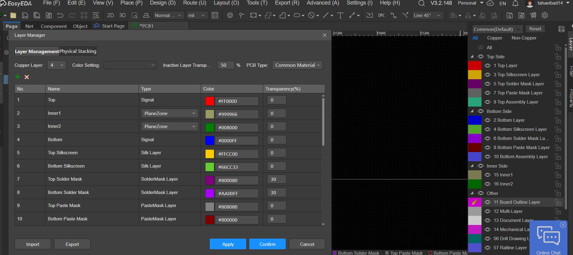
Configure multi-layer stackups in the EasyEDA Layer Manager for 4-layer designs.
This stackup is the workhorse of the industry for a reason. Every signal trace on the top or bottom layer has an adjacent solid ground plane, providing a well-defined return path and enabling controlled impedance routing.
The key principle here is: every signal layer should be immediately adjacent to a solid reference plane. When a signal trace switches layers through a via, the return current must also transition between reference planes. If those planes are at different potentials (e.g., one is GND and the other is VCC), you need stitching capacitors near the via to provide a low-impedance path for the return current at high frequencies.
Step-by-Step Walkthrough for Routing in PCB
Phase 1: Prioritizing Critical Signals
Not all nets are created equal. Before you start routing, you need to identify your critical nets and establish a routing priority hierarchy. Routing your critical paths first — while the board is still "open" and uncrowded — gives them the shortest, cleanest paths and the best impedance control.
A typical PCB trace routing sequence is shown below. The exact priority depends on the design, but critical power, high-speed, and sensitive analog circuits should always be routed before general-purpose signals.
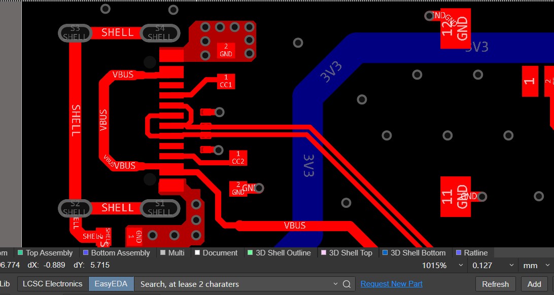
Prioritize critical pcb trace routing in EasyEDA for high-speed signals.
-
Critical Power Networks
Route high-current power loops and switching regulator circuits first. Minimize switching loop areas and ensure short return paths.
-
Critical High-Speed Signals
Route the most timing-sensitive and impedance-controlled signals first, including differential pairs (USB, PCIe, Ethernet, HDMI, LVDS), clock signals, DDR/SDRAM interfaces, and high-speed ADC/DAC interfaces. Maintain continuous reference planes, controlled impedance, and required length matching.
-
Sensitive Analog Signals
Route low-level analog signals, reference voltages, amplifier inputs, and feedback networks away from noisy digital and power circuits.
-
Remaining Digital Signals
Route general digital buses, GPIOs, control signals, LEDs, switches, and configuration pins.
-
Power Distribution Cleanup
Complete remaining power routing, copper pours, decoupling connections, and optimize return-current paths.
Phase 2: Partitioning and Functional Isolation
Once your critical nets are identified, the next step is to ensure that different functional sections of your board are physically and electrically isolated from each other. This is where your layout strategy becomes a routing strategy.
The goal is simple: keep noisy circuits away from quiet circuits, and make sure every current has a clean, uninterrupted return path through a solid ground plane beneath it.
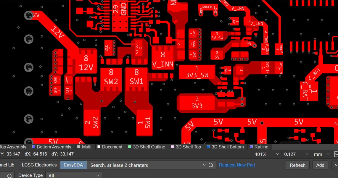
Plan functional isolation and component partitioning in EasyEDA for clear return paths.
1Digital/Analog Partitioning
If your board contains both digital circuits (microcontrollers, FPGAs) and sensitive analog circuits (ADCs, sensor amplifiers, voltage references), you should partition them into separate physical zones on the board. Route digital signals through the digital zone and analog signals through the analog zone. The two zones should share a single, solid ground plane — do NOT split the ground plane between digital and analog sections unless you are absolutely certain about the return current paths. A split ground plane, if done incorrectly, forces return currents to detour around the split, creating large loop areas that act as antennas.
2Power Section Isolation
Switching power supplies generate significant high-frequency noise. Isolate the switching regulator section physically and route the high-current switching loop (input cap → high-side FET → inductor → output cap → ground return) as a tight, compact polygon on the top layer. Keep this loop away from sensitive signal traces.
The continuous return path principle deserves repeating: when a signal trace transitions from the top layer to the bottom layer through a via, the return current on the ground plane must also transition. Place ground-stitching vias near every signal via to provide this return path. This is not optional for high-frequency designs — it is a fundamental requirement.
Phase 3: Setting Routing Rules and DRC in EasyEDA
The routing constraints you set in your EDA tool must align with your manufacturer's actual production capabilities. If you design 3-mil traces on a standard-process order, your board will either be rejected or manufactured with reduced yield and higher defect rates.
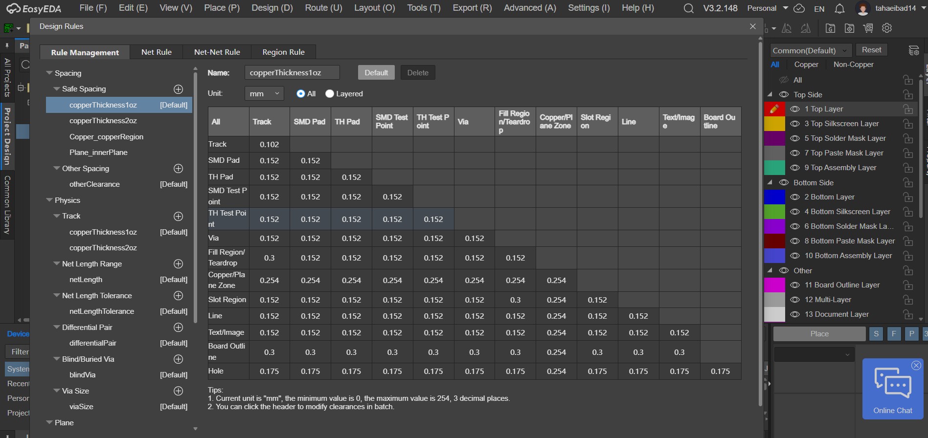
Configure routing rules and DRC settings in EasyEDA to match manufacturing capabilities.
1Configuring Design Rules in EasyEDA
EasyEDA allows you to set global and net-class-specific design rules that the router (and the DRC checker) will enforce. Here is how to configure them for JLCPCB's capabilities:
- Open your PCB design in EasyEDA.
- Navigate to Design → Design Rules (or press the Design Rules shortcut).
- Set the global defaults based on your intended JLCPCB fabrication process:
| Parameter | JLCPCB Standard (1–2 Layer PCB) | JLCPCB Standard (4+ Layer PCB) |
|---|---|---|
| Minimum Trace Width | 4 mil (0.100 mm) | 3.5 mil (0.09 mm); 3 mil with extra cost |
| Minimum Trace Spacing | 4 mil (0.100 mm) | 3.5 mil (0.09 mm); 3 mil with extra cost |
| Via Hole to Hole Spacing | 0.20 mm | 0.20 mm |
| Soldermask to Trace Clearance | ≥ 0.09 mm | ≥ 0.09 mm |
| PTH Annular Ring (min) | 0.25 mm (abs. min 0.18 mm) | 0.20 mm (abs. min 0.15 mm) |
| Solder Mask Expansion | 1:1 | 1:1 |
For specific net classes (e.g., power nets that carry higher current), create custom rules with wider trace widths. For example, set your VCC and GND net class to a minimum of 15–20 mil trace width.
2Running DRC (Design Rule Check)
After routing is complete (or even during routing — run it often), execute the DRC to catch violations before you submit your Gerber files:
- Navigate to Design → Design Rule Check in EasyEDA.
- Click Run DRC. The tool will scan your entire design against the rules you configured.
- Review the error list. Common violations include:
- Clearance violations — traces or pads that are too close together.
- Unrouted nets — connections that were missed during routing.
- Trace width violations — trace narrower than the minimum you specified.
- Via annular ring violations — vias with copper rings too small for fabrication.
Fix each violation and re-run the DRC until you get a clean pass. A clean DRC is not a guarantee of a perfect board, but a board with DRC errors is a guaranteed headache.
PCB Routing Checklist
Before you hit that "Generate Gerber" button and submit your design for fabrication, walk through this checklist.
1Placement
Components grouped by function (power, digital, analog, RF), decoupling caps adjacent to every IC power pin, connectors at board edges, nothing overlapping, and hot/noisy sections kept clear of sensitive circuits.
2Constraint Rules
Trace width/spacing meets JLCPCB minimums (4/4 mil 2-layer, 3.5/3.5 mil multilayer at 1 oz), net classes cover power, 50/90/100 Ω impedance, and diff pairs, vias respect 0.15/0.25 mm hole/diameter minimums, and nothing exceeds fab limits.
3Routing & Signal Integrity
Critical signals (power loops, diff pairs, clocks, analog) routed first with 45° bends or arcs over unbroken reference planes, stitching vias at layer changes, diff pairs spaced and length-matched, and serpentines at 3W–4W to avoid self-coupling.
4Power Design
Copper sized for expected current per IPC-2152 (≤ 10–20 °C rise), switching loops kept tight, at least one decoupling cap near every IC, power-plane splits don't break return paths, and high-current paths use parallel vias.
5DFM
Board within 670 × 600 mm for 2-layer FR4, copper-to-edge ≥ 0.2 mm (routed) or ≥ 0.4 mm (V-cut), silkscreen-to-pad ≥ 0.15 mm, text ≥ 40 mil (1.0 mm), via spacing ≥ 0.2 mm, and no acute angles that trap acid.
6DRC
Zero errors: no clearance, unrouted-net, trace-width, or annular-ring violations across all net classes, and DRC rerun after every significant routing change.
7Final Output & DFT
Gerbers verified in an external viewer with all layers aligned, mask openings match pads, drill file lines up, test points are probe-accessible, and board outline plus dimension layers are present and correct.
Crucial Engineering Considerations for Routing in PCB Design
Passing DRC is the minimum bar. Building a board that actually performs well in the real world requires a deeper understanding of two things that many designers underestimate: signal integrity and via parasitics. Let us dig in.
Maintaining Signal and Power Integrity (SI / PI)
Signal integrity (SI) is the art and science of ensuring that the voltage waveform that arrives at the receiving end of a trace looks like the waveform that left the transmitting end. Power integrity (PI) means making sure that every IC on the board sees a clean, stable supply voltage — even during transient current demands.
The Return Path Problem
Every signal current has a return current. In low-frequency circuits, that return current flows through the ground trace (or plane) by the most direct resistance path. But at higher frequencies — and "higher" starts lower than most people think — the return current flows through the ground plane directly underneath the signal trace, following the path of least inductance.
This is why ground planes matter so much. If you route a high-speed signal over a ground plane that has a slot or split directly beneath the trace, the return current must detour around that gap. The detour increases the loop area, which increases the loop inductance, which causes voltage ringing and radiated EMI. The signal might still "work" on the bench, but you will fail EMC certification and spend weeks debugging why.
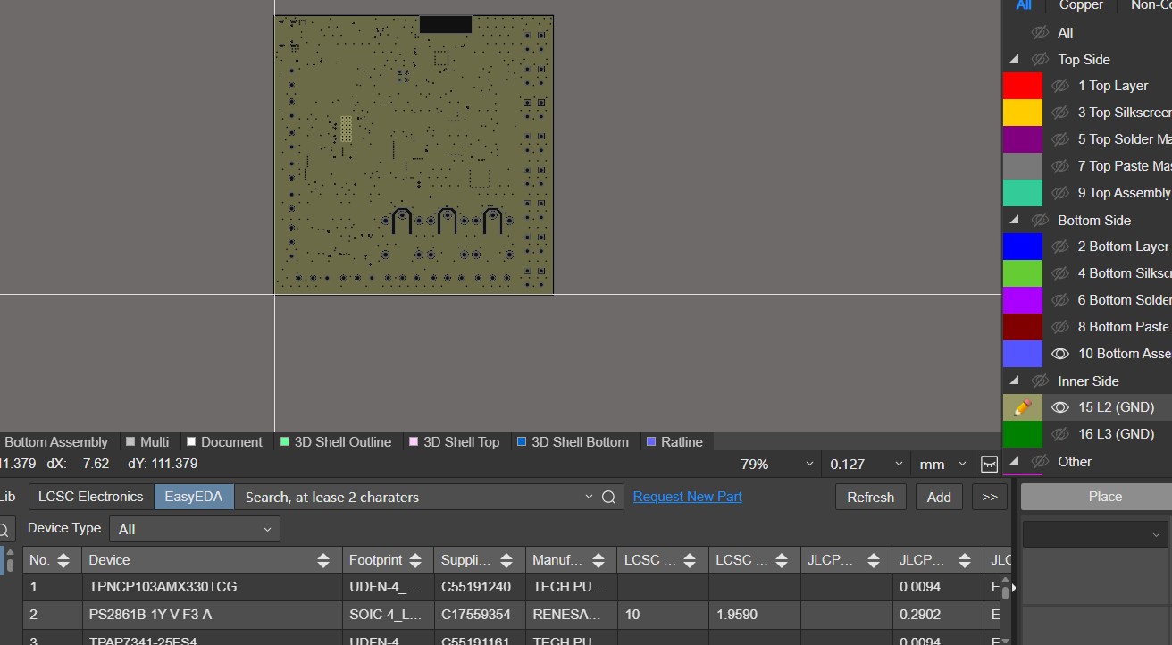
Verify continuous ground planes in EasyEDA to prevent signal return path detours.
Impedance Continuity
For high-speed signals (USB, HDMI, PCIe, DDR, Ethernet), the trace is not just a wire — it is a transmission line. The characteristic impedance of that transmission line is determined by the trace width, the distance to the reference plane, and the dielectric constant of the PCB substrate.
When a signal encounters an impedance discontinuity — a sudden change in trace width, a via, a connector pad, a stub — part of the signal energy reflects back toward the source. These reflections degrade the signal quality at the receiver and can cause timing errors, false triggering, and data corruption.
Maintaining impedance continuity means keeping the trace geometry consistent along the entire path, minimizing the number of vias, and using appropriate termination strategies (series, parallel, or AC termination) at the receiver end.
Managing Vias and Parasitics
Vias are necessary but imperfect. Every via introduces parasitic inductance and parasitic capacitance that degrade signal quality, and understanding these effects is essential for making informed routing decisions.
1Analysis of Via Parasitics
Via structures introduce parasitic inductance and capacitance due to the physical geometry of the via barrel, pads, anti-pads, and surrounding PCB layers. These parasitic effects create impedance discontinuities that can cause reflections, overshoot, undershoot, ringing, and waveform distortion in high-speed designs.
Parasitic Inductance (Lvia): The via barrel behaves like a small inductor. Longer vias and smaller barrel diameters generally increase parasitic inductance. The resulting impedance discontinuity can introduce signal integrity problems such as reflections, overshoot, undershoot, and ringing.
Parasitic Capacitance (Cvia): The via pad and surrounding anti-pad form capacitance to nearby power and ground planes. Larger pads, smaller anti-pad clearances, and smaller dielectric spacing between the via and reference planes generally increase parasitic capacitance. Together with via inductance, this capacitance contributes to impedance discontinuities and signal distortion at high frequencies.
2Best Practices for Via Reduction and Layer Transitions
Minimize Total Via Count: Keep high-speed signals such as USB, PCIe, and high-speed clock lines on the same routing layer whenever possible. Critical signal paths should minimize unnecessary vias to reduce discontinuities.
Provide a Nearby Return Path (Stitching Vias): When a signal changes layers, its return current must maintain a continuous low-inductance path. If the reference plane changes, place ground stitching vias close to the signal via. The exact spacing depends on signal edge rate, stackup, and application requirements.
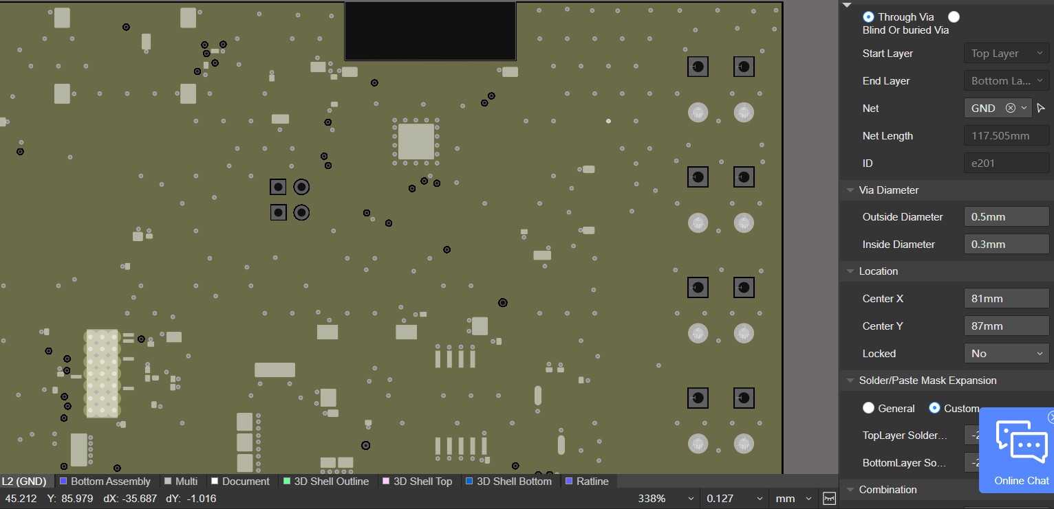
Place ground stitching vias in EasyEDA to maintain a continuous return path.
Optimize Via Dimensions: Use the smallest via structure that meets manufacturing capability. Smaller via structures generally reduce parasitic discontinuities. For example, a 0.2 mm drill / 0.4 mm pad via typically introduces less parasitic effect than a 0.3 mm drill / 0.6 mm pad via.
Remove Via Stubs: Unused portions of through vias extending beyond the signal layer behave as resonant transmission-line structures and can create reflections at high frequencies. For high-speed multilayer designs, consider blind vias, buried vias, or back drilling to reduce or eliminate via stubs.
Key Engineering Notes
Via parasitics become increasingly important as signal rise time decreases.
High-speed design decisions should consider edge rate, not only clock frequency.
Maintaining a continuous reference plane is often more important than simply reducing via count.
Return current path continuity is essential for signal integrity and EMI control.
Advanced Techniques for PCB Trace Routing: Beyond the Basics
The foundational rules we have covered so far will get you through the majority of PCB designs. But as clock speeds increase and signal rise times decrease, additional techniques become necessary.
Right-Angle Alignment
You have probably heard the rule: "never use 90-degree corners in trace routing." But do you know why?
When a trace makes a sharp 90-degree turn, the effective width of the copper at the corner increases to approximately 1.414× the trace width. This creates a localized impedance discontinuity — the wider cross-section lowers the impedance momentarily, causing a minor signal reflection. For general-purpose digital signals below 1 GHz, the effect is honestly negligible in practice. However, it remains standard PCB routing best practices to use 45-degree mitered corners or smooth arc bends for two good reasons: it avoids the (small) impedance bump, and it prevents potential acid traps during the etching process where etchant can pool in sharp inside corners and over-etch the copper.
Bottom line: use 45-degree angles or arcs. There is no cost or downside, and it is simply good engineering practice.
Differential Traces
Differential pairs — where a signal is transmitted as the voltage difference between two complementary traces (D+ and D−) — are used extensively in modern high-speed interfaces like USB, HDMI, LVDS, and Ethernet.
When routing differential pairs, maintain consistent spacing between the two traces, keep them tightly coupled over their entire length, and match their lengths to within the specification required by the interface. EasyEDA provides differential pair routing tools that enforce coupling and length matching automatically.
Important
Differential pairs still need a solid ground return path beneath them. The common-mode component of the signal still returns through the reference plane, and a broken or split plane under a differential pair will degrade common-mode rejection and increase EMI — defeating one of the primary advantages of differential signaling.
Serpentine Lines
Serpentine routing (also called length tuning or meander routing) is used when two or more signals that are part of a parallel bus must arrive at the receiver within a specific time window of each other.
The serpentine pattern adds extra trace length to the shorter nets so they match the length of the longest net in the group. The key design rule when creating serpentine patterns is spacing: maintain at least 3W to 4W spacing (where W is the trace width) between the parallel segments of the serpentine to prevent self-coupling crosstalk within the meander. If the segments are too close, the magnetic fields from adjacent segments partially cancel each other out, effectively reducing the delay added by the extra length — which defeats the purpose of the length tuning.
FAQ about PCB Routing Rules
Q: Is PCB routing hard?
Honestly? The basics are straightforward — connect point A to point B with a copper trace. But mastering PCB routing to the point where your boards consistently work on the first spin, pass EMC, and have no thermal or signal integrity issues? That takes experience, and a healthy respect for the physics involved. The good news is that modern EDA tools like EasyEDA handle a lot of the complexity for you (auto-routing, DRC, impedance calculators), and following the PCB routing rules in this article will get you 90% of the way there. The remaining 10% comes from building boards, debugging them, and learning from each iteration.
Q: How does the 3W rule relate to IPC standards?
The 3W rule is an industry guideline, not an official IPC-mandated requirement. It originated from empirical observations and field studies on crosstalk reduction and has been widely adopted as a practical spacing guideline. The formal standards for trace spacing and clearance are defined in IPC-2221 for voltage-based clearance requirements and interface-specific standards. The 3W rule is essentially a convenient shorthand for ensuring adequate electromagnetic isolation between adjacent signal traces.
Q: What is the minimum trace width I can use with JLCPCB?
For standard 1–2 layer PCB orders, JLCPCB supports a minimum trace width of 4 mil (0.10 mm). For multi-layer boards using advanced fabrication processes, the minimum drops to 3.5 mil (0.09 mm). However, designing to the absolute minimum is not recommended for production designs — it reduces manufacturing yield and leaves no margin for process variation. A safer approach is to use 8–10 mil for signal traces and 15+ mil for power traces, going tighter only where the design absolutely demands it (such as BGA fan-out).
Q: Should I use auto-routing or route manually?
For professional designs, manual routing of critical nets is always recommended. Auto-routers have improved significantly over the years, and EasyEDA's auto-router can handle simple boards reasonably well. However, auto-routers do not understand your circuit's function — they do not know which traces are clock signals, which are sensitive analog inputs, and which carry high current. The recommended approach is to manually route all critical signals first (clocks, differential pairs, power loops, sensitive analog), and then use the auto-router for the remaining non-critical general-purpose connections, followed by a thorough manual review and cleanup.
Q: How many vias are too many?
There is no fixed number — it depends entirely on the design. A four-layer board will naturally have more vias than a two-layer board, and that is expected and acceptable. The concern is not the total via count, but the via density in critical signal paths. For high-speed signals, minimize layer transitions to reduce parasitic inductance and capacitance. For power distribution, multiple vias in parallel are actually desirable because they reduce the effective resistance and inductance of the power path. The rule of thumb: use as many vias as your power distribution needs, and as few as your signal integrity requires.
Conclusion: PCB Routing Rules
Efficient PCB routing is the art of balancing space planning, circuit performance, and physical manufacturing constraints. There is no single trick or shortcut — a successful routing project emerges from a disciplined process: start with a thoughtful component placement that reflects your circuit's signal flow, apply the core PCB routing rules for trace width, spacing, and layer stackup, prioritize critical signals first, maintain continuous return paths, verify your design against manufacturer capabilities through DRC.
The best routed board is not the one with the tightest traces or the most clever via stitching. It is the one that works reliably on the first prototype, passes EMC testing without surprises, and is manufacturable at scale without yield issues. Master these PCB routing rules, and that board will be yours.
Keep Learning
Demystifying PCB Trace Length Matching vs Frequency: Ultimate Guide
Key Takeaways Signal rise time, not clock frequency, is the true determinant of trace length matching tolerance. A 10 MHz clock with a 100 ps rise time behaves like a GHz signal and demands strict matching. Dielectric dispersion causes phase velocity to shift across the spectrum, invalidating single-frequency matching assumptions. Designers should match by time-domain delay in picoseconds, not by physical length in mils. Serpentine routing suits single-ended traces, while sawtooth tuning preserves cou......
Bias Tee Design and PCB Layout: Guide for RF Engineers
Key Takeaways A bias tee lets DC power and an RF signal share one trace, using just an inductor and a capacitor. No separate DC line needed. Pick L and C using two simple rules: the inductor's reactance should be at least 10x the system impedance, and the capacitor's reactance should be at most one tenth of it. Layout matters as much as the math. A few extra millimeters of trace at the L-C junction can shift the whole frequency response. Three habits keep a bias tee working as designed: controlled imp......
PCB Routing Rules: Essential Guidelines & Best Practices
Key Takeaways 1. Placement Drives Routing: Good component placement, grouped by functional block with decoupling caps adjacent to IC power pins, determines 70% of routing success before the first trace is drawn. 2. Master Trace Width & Spacing: Size traces per IPC-2152 for current-carrying capacity and maintain center-to-center spacing of at least 3W between adjacent traces to suppress crosstalk. 3. Build a Solid Layer Stackup: Every signal layer must sit adjacent to a continuous reference plane to de......
PCB Teardrop You Should Know
In the design and manufacturing of PCBs (Printed Circuit Boards), the teardrop (Pad Tear Drop) plays a vital role. It is not only the connection point between electronic components and PCB, but it can also enhance the soldering strength and improve stability. This article will delve into what a PCB teardrop is, what it does, and how to set up a PCB teardrop to help you better understand and apply this key technology. What is a PCB Teardrop? PCB teardrops are small drops of solder material that form ar......
Mastering PCB Routing Techniques for Optimal Circuit Design and Performance
Introduction PCB routing is a fundamental and intricate aspect of circuit design that significantly influences the performance, reliability, and functionality of electronic devices. Effective PCB routing techniques are critical for optimizing electrical traces, maintaining signal integrity, and ensuring the overall efficiency of the PCB layout. This comprehensive guide will explore various PCB routing techniques, from trace optimization and signal path management to high-speed PCB routing and layout d......