How to Design Your Own Keyboard PCB: From Layout to Firmware
16 min
- What You Need to Build a Custom Keyboard PCB
- Step 1: Choose Compatible Switches and PCB Footprints
- Step 2: Design the Keyboard Matrix and Add Diodes
- Step 3: Select the MCU and Design the USB Interface
- Step 4: Plan Stabilizer Locations and Mechanical Features
- Step 5: Draw the Keyboard Schematic (Step by Step)
- Step 6: Lay Out and Route the PCB
- Step 7: Flash the Firmware and Test the Keyboard
- Step 8: Order & Assemble Your Keyboard PCB from JLCPCB
- FAQs about Custom Keyboard PCB Design
- Conclusion
Designing a custom keyboard PCB is one of the most rewarding entry points into practical electronics. You not only get a really useful product on your desk, but also you learn schematic capture, matrix scanning, footprint selection, USB, and firmware. Most of the hardware engineers use the same skills that show up on professional boards.
This guide walks the entire build from choosing switches, wiring the diode matrix, adding the microcontroller and USB-C, laying out the board, and flashing QMK or VIA firmware.
Whether you want a compact 65% board, an ortholinear grid, or a full-size layout, the underlying engineering is the same. Let's build it step by step.
What You Need to Build a Custom Keyboard PCB
If you just want the shopping list and the roadmap before diving into theory, start here:
Keyboard PCB Parts and Tools Checklist (Starter BOM)
A realistic starter bill of materials for a single-PCB mechanical keyboard. Quantities scale with your key count; this table assumes a ~65-key board.
| Part | Example | Qty | Notes |
|---|---|---|---|
| Mechanical switches | Cherry MX / Gateron / Kailh | 1 per key (65) | 5-pin PCB-mount footprint accepts both 3 and 5-pin switches |
| Signal diodes | 1N4148 (THT) or 1N4148W SOD-123 | 1 per switch | One diode per key |
| Microcontroller | ATmega32U4 (Pro Micro) or RP2040 | 1 | Native USB |
| USB connector | USB-C receptacle (16-pin) | 1 | Add two 5.1 kΩ CC pull-downs |
| CC resistors | 5.1 kΩ 0402/0603 | 2 | Device-side (sink) detection |
| Decoupling caps | 100 nF X7R + 1–10 µF bulk | 5–8 | One 100 nF per supply pin |
| ESD protection | TVS diode array | 1 | On D+/D- and VBUS |
| Hot-swap sockets (optional) | Kailh MX hot-swap socket | 1 per key | Solder to the back; no switch soldering later |
| Stabilizers | PCB-mount or plate-mount | 5 | For Backspace, Enter, Shift, Spacebar |
| Plate + case | Aluminum/FR-4 plate + case | 1 set | Holds switches; sets rigidity |
Keyboard PCB Design Workflow at a Glance: 8 Essential Steps
- Define the keyboard PCB layout: Use the keyboard Layout Editor to get exact key coordinates and choose the arrangement.
- Choose switches & footprints: MX 5-pin, Choc, or hot-swap; this sets your footprint library.
- Design the diode matrix: Wire switches into rows × columns with one diode per key.
- Add the MCU & USB: Microcontroller, USB-C, CC resistors, ESD, decoupling.
- Draw the keyboard PCB schematic: Switches, diodes, matrix nets, and the support circuit.
- Layout the PCB: Place switches in the key grid, route columns and rows.
- Flash firmware & test: QMK or VIA, then check every key.
- Order fab + assembly: Export Gerbers, BOM, and CPL, then send to JLCPCB for instant quote.
Keyboard PCB Design Cost, Time, and Skill Requirements
This is an intermediate project; if you've drawn a schematic and routed a simple two-layer board before, you can do it. The first design may take up to 2-3 days in KiCad or EasyEDA, plus fabrication lead time. A first custom keyboard PCB typically lands around $40–$120 all-in for a small run of boards plus switches, diodes, stabilizers, and a controller.
Step 1: Choose Compatible Switches and PCB Footprints
Your switch choice drives your footprint choice, and the footprint you place in your EDA library determines which physical switches will actually fit.
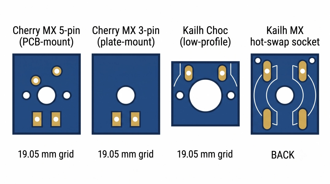
Figure: Switch-footprint comparison
Cherry MX (3-pin plate-mount vs 5-pin PCB-mount)
The Cherry MX style is the de facto standard, and Gateron, Kailh, and others clone the same stem and pinout. Two mounting variants exist:
- 3-pin (plate-mount): A center post plus two electrical pins. These rely on a plate to stay aligned, with no plastic legs gripping the PCB.
- 5-pin (PCB-mount): The center post and two electrical pins plus two plastic alignment legs that snap into the board, so the switch sits square even without a plate.
Kailh Choc (low-profile)
For a slim, laptop-like board, Kailh Choc v1 switches are the low-profile option. They're shorter and use a completely different footprint and pin spacing. It is roughly an 18 × 17 mm key spacing versus the MX 19.05 mm standard, so MX and Choc are not interchangeable.
Hot-swap Sockets vs. Soldered Switches
You can either solder switches permanently into the board or add Kailh MX hot-swap sockets. That lets users push switches in and pull them out with zero soldering. Here is a quick comparison of hot-swap and soldered PCBs.
| Criterion | Hot-swap PCB | Soldered PCB |
|---|---|---|
| Switch changes | Anytime, no tools | Requires desoldering |
| Cost | Higher (socket per key) | Lower |
| Board profile | Slightly taller (socket on back) | Lower, more rigid feel |
| Beginner friendliness | High — no switch soldering | Needs soldering skill |
| Reliability | Socket wear over many swaps | Permanent, most robust |
| Assembly | SMT sockets ideal for PCBA | THT or SMD switches |
Step 2: Design the Keyboard Matrix and Add Diodes
This is the single most important electrical concept in keyboard design, and the section that separates a board that works from one with phantom keypresses.
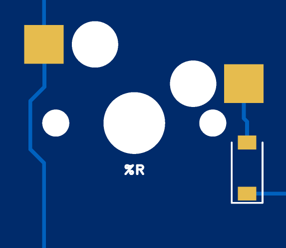
Figure: One key's unit cell: the large center post hole, two switch pin pads, and the SOD-123 diode pad.
Understand Keyboard Matrix (Rows × Columns)
There are approximately 104 keys on a full-size keyboard. Connecting 1 pin of the MCU per key would require 104 GPIOs, and this is not possible.
Clearly, keyboards employ a matrix method where the switches are arranged in an M × N grid of rows and columns, and the MCU requires just (rows + columns) pins. A 104-key board can be comfortably accommodated in an 8 × 14 matrix and needs only 22 pins to control instead of 104.
The MCU scans the matrix: it turns on one line (energizes a column) and sees if there is any line that is on (connected rows). It walks through each column in turn thousands of times per second and debounces each key in firmware to handle contact bounce. When the energized column intersects with the pressed switch, current gets to a row, and we get a keypress.
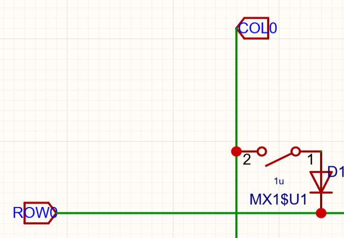
Figure: The schematic of a single matrix cell: COL0 connects to the switch, the switch connects through diode D1 to ROW0.
Why Keyboard Ghosting Happens?
The sneak-path problem.
Here's the problem the matrix creates. Imagine three keys are pressed in a rectangle pattern. When you energize a column to read it, current doesn't flow only in the intended single direction; it finds a sneak path, and the MCU sees it as a phantom fourth key. That false reading is ghosting; the related failure where a real key gets hidden is masking.
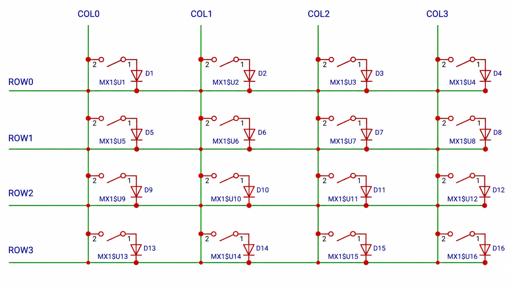
Figure: A 4×4 keyboard matrix with one diode per switch.
Use Diodes to Prevent Ghosting
The fix is elegant: put a diode in series with every switch so current can only flow one way, a diode is a one-way valve. With one diode per key, the reverse sneak path is blocked, so only the keys you actually press conduct.
That's what enables reliable N-key rollover (NKRO): press as many keys at once as you like and every one registers.
The practical rules:
- Use a 1N4148 small-signal diode. Use a through-hole 1N4148 (DO-35 body); for SMD, use 1N4148W (SOD-123) or the smaller 1N4148WS (SOD-323).
- One diode per switch.
- All diodes in the same orientation. In this reference design, the diode cathode faces the ROW line, the configuration known as QMK. A single reversed diode gives you a dead key that's maddening to debug.
Step 3: Select the MCU and Design the USB Interface
The MCU is the brain: it scans the matrix, debounces, applies your keymap, and presents itself to the computer as a standard USB HID keyboard.
Choosing an MCU (ATmega32U4 / Pro Micro vs RP2040 vs others)
You want a microcontroller with native USB, so you don't need a separate USB-to-serial chip. Some other MCUs with the practical routes are:
| MCU | Native USB | QMK support | Notes |
|---|---|---|---|
| ATmega32U4 | Yes | First-class | The classic beginner choice |
| RP2040 | Yes | Yes, well supported | Cheaper, far more powerful |
| STM32 (e.g. F072/F411) | Yes | Yes | More GPIO |
| CH552 | Yes | Community | Ultra-low-cost |
For a first board, an ATmega32U4 is the safest path because QMK support is rock-solid. RP2040 is the modern choice; it is cheaper, faster, and better supported.
USB-C Wiring and ESD/CC Resistors
USB-C is the modern standard, but there's one detail people miss. For a device (a sink like a keyboard), each CC pin (CC1 and CC2) needs its own 5.1 kΩ pull-down resistor to GND. Without them, a USB-C host won't detect the keyboard or supply the 5 V rail.
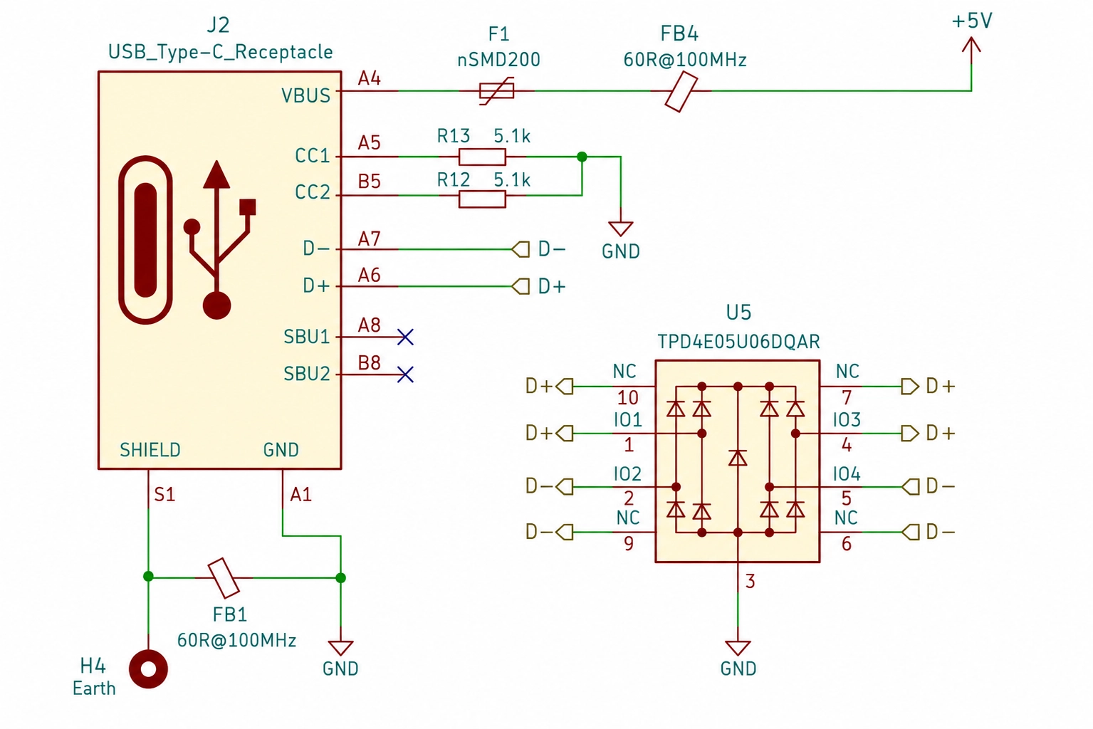
Figure: USB-C device wiring: each CC pin (CC1 and CC2) gets its own 5.1 kΩ pull-down to GND
Also, add ESD protection to the D+ / D- data lines and VBUS; a small TVS diode array protects the MCU from static discharge whenever someone plugs in.
Other Supporting Circuitry (Decoupling, Reset, Boot/Crystal)
A microcontroller needs a small support circuit around it:
- Decoupling: A 100 nF capacitor on each power pin, as close to the pin as possible, plus one bulk capacitor (1–10 µF) on the rail.
- Reset: A reset (or reset + boot) button to force the chip into its bootloader for flashing.
- Clock: the ATmega32U4 uses a 16 MHz crystal with two load caps; the RP2040 uses a 12 MHz crystal.
Step 4: Plan Stabilizer Locations and Mechanical Features
Wide keys like spacebar, Enter, Backspace, and the Shifts are too long to ride on a single switch stem without wobbling. Stabilizers hold them level.
PCB-mount vs Plate-mount Stabilizers
- PCB-mount stabilizers mount directly to the board, so your PCB needs the correct stabilizer cutouts in the footprint.
- Plate-mount stabilizers clip into the plate instead. They're simpler but generally feel less stable than a screwed-in PCB-mount set.
Stabilizer Sizes and Placement
Stabilizer size is named by key width in units ("u"), where 1u is one standard key:
- 2u for the backspace, Enter, and the Shift keys (and often numpad +/Enter).
- 6.25u or 7u for the Spacebar (6.25u is most common on modern layouts)
Place stabilizer cutouts precisely according to the layout spec. If the wire spacing is even slightly off, the stabilizer bar may bind.
Step 5: Draw the Keyboard Schematic (Step by Step)
With the chosen parts, draw the schematic in an EDA tool.
KiCad and EasyEDA are both free and export cleanly to JLCPCB. (The reference Mikeneko 65 is drawn in EasyEDA.)
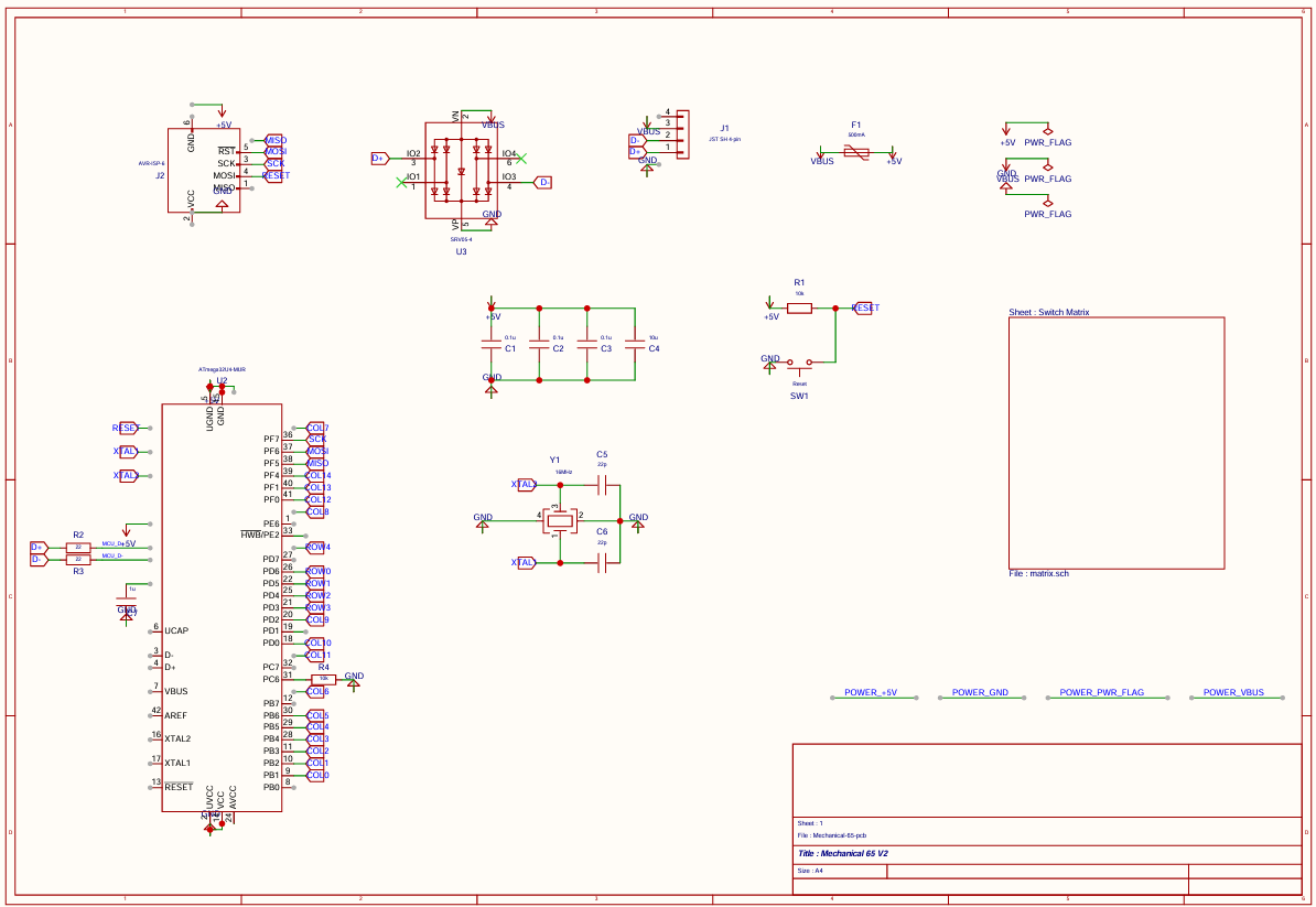
Figure: Schematic sheet 1: contains the main microcontroller
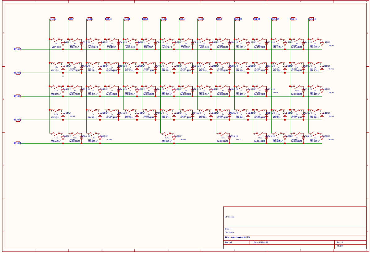
Figure: Schematic sheet 2: For switch matrix
Placing Switches, Diodes, and the Matrix
- For each key, drop a switch symbol and its series diode. That switch-plus-diode pair is your matrix "unit cell."
- Connect every switch's free pin to its column net (COL0, COL1, …).
- Connect each diode's cathode to its row net (ROW0, ROW1, …)
- Repeat across the grid so each column and each row is a single shared net.
- Wire each row and column net to a dedicated MCU GPIO, and record the pin assignments.
- Wire the USB-C connector: VBUS to the 5 V rail (through ESD/TVS), D+ / D- to the MCU's USB pins, and a 5.1 kΩ pull-down on each CC pin.
- Add the decoupling capacitors, reset button, and crystal, then run the schematic's Electrical Rules Check (ERC) to catch unconnected pins before you touch the layout.
Step 6: Lay Out and Route the PCB
Layout is where a keyboard PCB differs from a generic board: switch positions are not yours to move freely, but the key grid fixes them.
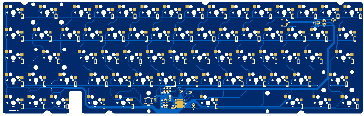
Figure: Back side of the same board
Place switches first, and lock them to the key layout. Import your Keyboard Layout Editor coordinates, so every switch lands exactly on the 19.05 mm grid. Going hot-swap? The socket footprints sit on the back. Then drop each diode next to its switch. Keeping the diode in the same spot at every keypress makes routing cleaner and more consistent.
Routing the Matrix (Columns Vertical, Rows Horizontal)
The classic, reliable strategy on a standard 2-layer, 1.6 mm FR-4 board:
- Route columns vertically and rows horizontally. Running perpendicular to each other, they rarely fight for space.
- Where a row and column must cross, jump to the other copper layer (drop a via, cross on the bottom, come back up). This is exactly why two layers are enough.
- Use a sensible trace width (0.25 mm/10 mil is plenty for logic-level matrix signals), add a ground pour for a clean return and easier manufacturing, and keep clearances comfortable.
- Run a Design Rule Check (DRC) and confirm that there are no unrouted nets before exporting. Run a quick DFM sanity check against your fab's capabilities too, so nothing surprises you at manufacturing.
Step 7: Flash the Firmware and Test the Keyboard
Hardware is only half the board. It is the firmware that turns your matrix into keystrokes. The two names you'll hear are QMK and VIA.
What QMK and VIA Do and How They Differ
QMK is the open-source keyboard firmware that runs on the MCU. You configure it in code with matrix pins, diode direction, and keymap.
VIA is a graphical app that remaps keys at runtime with no recompiling, on firmware built to be VIA-enabled.
The key thing to understand: VIA still runs on QMK underneath. It isn't a competitor to QMK; it's a friendly front-end that reads a keyboard-definition JSON so the GUI knows your layout.
| Feature | QMK | VIA |
|---|---|---|
| What it is | The firmware on the MCU | A GUI that remaps a QMK board |
| Change keys | Edit code, recompile, reflash | Live in an app, instant |
| Needs coding | Yes (C-style config + keymap) | No |
| Setup | Define matrix, compile .hex/.uf2 | Load a keyboard definition JSON |
| Best for | Full control, advanced features | Fast, no-code remapping |
| Relationship | Runs on its own | Runs on top of VIA-enabled QMK |
Compile your firmware, and you get a flashable binary: a .hex file for AVR targets like the ATmega32U4, or a .uf2 file for the RP2040 (flashed by dragging it onto the board when it mounts as a USB drive). Put the board into bootloader mode with the reset button, flash, and you're done.
Step 8: Order & Assemble Your Keyboard PCB from JLCPCB
You've got a DRC-clean board. Now turn the design files into a physical PCB.
From KiCad or EasyEDA, export three sets of files:
- Gerbers + drill files
- BOM (Bill of Materials)
- CPL / Pick-and-Place file
Now you can turn the ideas into real products with JLCPCB’s end-to-end services, upload your Gerbers for an instant fabrication quote, then add PCB Assembly to have the diodes and hot-swap sockets placed for you.
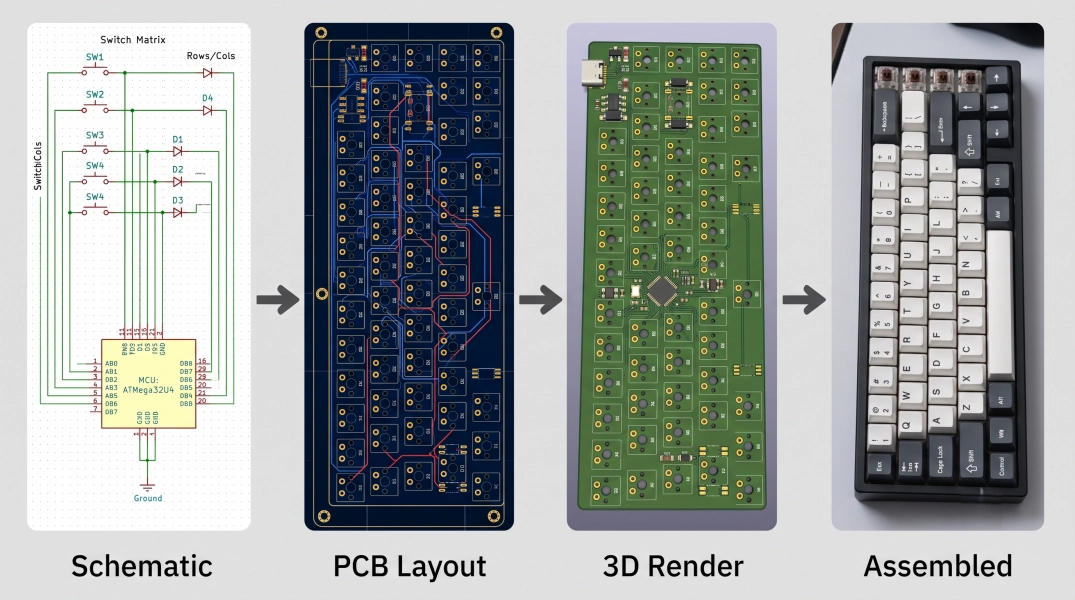
Figure: The design-to-product path every PCB follows: schematic > PCB layout > assembled board.
FAQs about Custom Keyboard PCB Design
Q: Do you really need diodes on a keyboard PCB?
If your keys are wired in a matrix, then yes. Without a diode in series with each switch, certain three-key combinations create a sneak that results in ghosting. One 1N4148 per switch, all facing the same way, blocks that path and gives you full N-key rollover.
Q: What microcontroller should I use for a custom keyboard?
Pick one that comes with native USB support. The ATmega32U4 is the classic beginner choice for its first-class QMK support. The RP2040 is the modern option with a cheaper, more powerful CPU.
Q: Hot-swap PCB or soldered PCB — which is better for beginners?
Soldered switches are cheaper, lower-profile, and the most robust, but changing one means desoldering. In this way, they are not repair-friendly, so if you don't want to do hard repairs, go for a hot-swap PCB.
Q: How much does it cost to make a custom keyboard PCB?
Bare-board fabrication is inexpensive, often only a few dollars per board on a small JLCPCB order. The real cost is the parts: switches, diodes, stabilizers, a controller, and optional hot-swap sockets. A complete first build usually lands around $40–$120.
Q: What software do I use to design a keyboard PCB?
For the board, KiCad or EasyEDA. Both are free, and both export Gerbers, BOMs, and CPLs that JLCPCB accepts. Use a Keyboard Layout Editor to define the physical arrangement and helper tools to place footprints.
Q: Can JLCPCB assemble hot-swap sockets and diodes for me?
Yes. With JLCPCB PCBA, upload your BOM and CPL alongside your Gerbers, and the SMT line places the SMD 1N4148W diodes and Kailh hot-swap sockets for you. One SMD diode per key is ideal for automated assembly, so you receive a populated board and just add switches and stabilizers.
Conclusion
Building a custom keyboard PCB comes down to eight repeatable steps: define your layout, choose switches and footprints, wire the diode matrix, add the MCU and USB-C, draw the schematic, lay out and route the board, order fabrication and assembly, then flash QMK or VIA and test.
The parts that feel intimidating at first, the matrix, ghosting, CC resistors, and diode direction, are really just a handful of clear rules you now know.
One 1N4148 per switch, all facing the same way, a native-USB MCU, 5.1 kΩ on each CC pin, columns vertical and rows horizontal, and firmware pins that match your schematic.
Big shoutout to maker Bishal Mondal, who shares the Mikeneko 65 PCB as an open-source project on OSHWLab (EasyEDA). You can see the other popular published builds, including the Frieren v1 mechanical keyboard, an ESP-based keyboard, and a QMK-ready keyboard project.
These open-source keyboards were designed in EasyEDA, manufactured by JLCPCB, and supported by the EasyEDA Spark Program, an initiative that helps makers turn their ideas into real hardware by providing PCB fabrication and component sponsorship.

Popular Articles
• AI Tools for PCB Design: Which Tool Fits Your Workflow Stage?
• GPT-6 Astra PCB Design in KiCad: From Brief to Verified Native Project
• GPT-6 Astra PCB Design in EasyEDA Pro: What Worked, What Failed, and What We Learned
• AI PCB Design: From Prompt to PCB with EasyEDA Pro
• How to Design Your Own Keyboard PCB: From Layout to Firmware
Keep Learning
GPT-6 Astra PCB Design in KiCad: From Brief to Verified Native Project
Key Takeaways What OpenAI published: The launch page features a 15-second condensed clip of GPT-6 Astra performing PCB layout in KiCad. What the model did: It turned a four-line brief into a 44 × 34 mm, two-layer PCB, covering the circuit, footprints, component placement, routing, and a native two-sheet schematic. Where the work went: Placement and routing were only part of the work. Two linked schematic sheets, project-local libraries, and UUID-based links between 45 components and their footprints w......
GPT-6 Astra PCB Design in EasyEDA Pro: What Worked, What Failed, and What We Learned
Key Takeaways What was tested: GPT-6 Astra was given access to a native EasyEDA Pro 3.2.149 installation and asked to design a stereo TPA3116D2 amplifier from a four-line written brief. What it produced: The run resulted in a 44 × 34 mm, two-layer PCB with 40 SMD components and an editable native EasyEDA Pro project with embedded libraries. Where it failed: The first complete import opened cleanly and looked plausible, yet the initial native verification reported 50 association mismatches involving 12......
AI Tools for PCB Design: Which Tool Fits Your Workflow Stage?
AI tools can now assist with PCB architecture, schematic generation, component selection, placement, routing, and design verification. However, different tools target different stages of the PCB workflow. This guide compares AI tools for PCB design based on what they actually do, what inputs they require, and where they fit within a real engineering workflow. In this guide, you will learn: The 6 types of AI PCB tools and the input each one needs What AI PCB design tools do, compared stage by stage How......
EasyEDA Pro vs KiCad: GPT-6 Astra PCB Design Compared
Key Takeaways What is being compared: Two versions of the same TPA3116D2 stereo amplifier project, each created by GPT-6 Astra in a different EDA tool. The comparison focuses on what you can actually do with the delivered project afterward. Ground copper: In the EasyEDA Pro project, the ground copper is stored as 28 fixed filled regions. In KiCad, it remains as two native copper zones that can automatically refill after layout changes. Verification: KiCad initially reported 46 schematic-parity issues.......
A Practical Guide to ODB Files for PCB Manufacturing
Key Takeaways All-in-One Data: ODB++ combines artwork, netlist, stackup, and drill spans in a single package. Fewer Errors: Embedded netlists allow CAM software to catch errors before production. Pre-Export Checks: Clear DRCs, close the board outline, and verify drill spans in a viewer. Best Practice: Use Gerber for quick quotes and keep ODB++ ready for engineering queries. A Gerber layer might simply say, “draw a 0.5 mm (20 mil) circle here.” ODB++ can describe that same feature as a pad on the VCC n......
AI PCB Design: From Prompt to PCB with EasyEDA Pro
Key Takeaways AI PCB design uses AI agents to automate schematic creation, component selection, layout, and verification inside a real EDA editor — not just generate images. The workflow connects EasyEDA Pro to an AI coding agent (Claude Code or Codex) through the EasyEDA API Gateway, the open-source API Skill, and a local bridge server. Setup takes about ten minutes and is fully local-first: designs, API calls, and intermediate code never leave your machine. Because the agent places real library part......