AI Tools for PCB Design: Which Tool Fits Your Workflow Stage?
17 min
- Types of AI Tools for PCB Design
- 10 AI Tools for PCB Design in 2026
- AI PCB Design Tools Compared
- How to Choose an AI Tool for PCB Design
- What Are the Limitations of AI PCB Design Tools?
- Conclusion
- FAQs About AI Tools for PCB Design

AI tools can now assist with PCB architecture, schematic generation, component selection, placement, routing, and design verification. However, different tools target different stages of the PCB workflow.
This guide compares AI tools for PCB design based on what they actually do, what inputs they require, and where they fit within a real engineering workflow.
In this guide, you will learn:
- The 6 types of AI PCB tools and the input each one needs
- What AI PCB design tools do, compared stage by stage
- How to choose a tool for your starting point and EDA software
- Why AI output still needs engineering verification
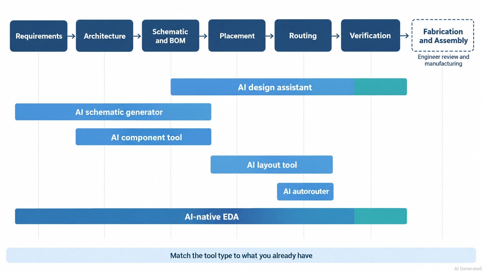
Figure: AI tools for PCB design mapped to each stage of the design workflow.
Types of AI Tools for PCB Design
AI PCB design tools fall into six types. To narrow the list, match the tool type to what you already have: an idea, requirements, a schematic, or a placed board.
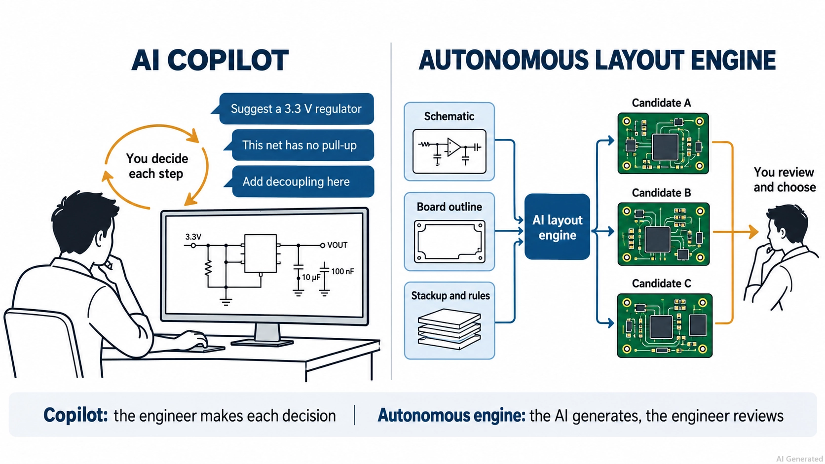
Figure: AI copilot compared with an autonomous layout engine in PCB design.
| Tool Type | Starting Input | AI Helps With | Typical Output | Examples |
|---|---|---|---|---|
| AI design assistant | Design question or existing project | Suggestions and review | Recommendations | Flux, EasyEDA Pro with an AI agent |
| AI schematic generator | Requirements or a text prompt | Architecture and schematic | Schematic and BOM | CELUS, Circuit Mind, ProtoFlow |
| AI component tool | Requirements or schematic | Part selection | Components and BOM | CELUS, Circuit Mind, Flux |
| AI layout tool | Schematic plus constraints | Placement and routing | PCB layout | Quilter, Cadence Allegro X AI |
| AI autorouter | Existing placed board | Routing | Routed PCB | DeepPCB, Flux AI Auto-Layout |
| AI-native EDA | Product requirements | Several stages in one tool | Native PCB project | Flux, JITX, ProtoFlow |
The tools also differ in how much control they take over the design process. For a cleaner, more technical flow: Copilot-style tools suggest changes and let you make each design decision. Autonomous layout engines, by contrast, can generate complete placement-and-routing candidates from your constraints, which you then review and refine.
10 AI Tools for PCB Design in 2026
These 10 tools cover the workflow from requirements to routing. Their selection is not based on rank; the right choice depends on your starting input and the EDA software you use.
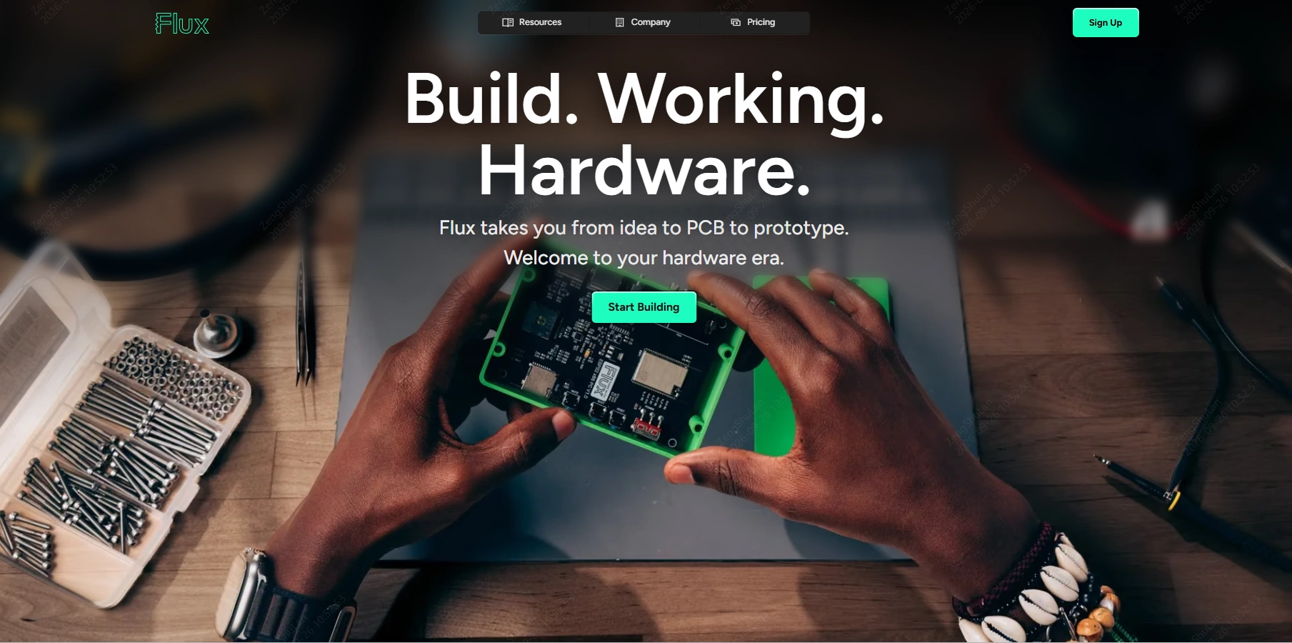
1. Flux
Flux is a browser-based PCB design tool built around an AI agent. It is best suited for makers, startups, and small teams that want one tool from idea to routed board.
Flux can plan the design, find in-stock parts, wire the schematic, place parts, route, and run ERC and DRC as it works.
- Input: A plain-language brief with goals, constraints, interfaces, and preferred parts.
- Output: An editable Flux project with Gerber, drill, BOM, and pick-and-place files.
- PCB workflow stage: Requirements through layout.
Key limitation: Flux positions AI Auto-Layout for simple to medium-complexity boards. But critical traces may need manual routing.
Learn more: How to Design a PCB with Flux.ai (Step-by-Step Guide)
2. Quilter
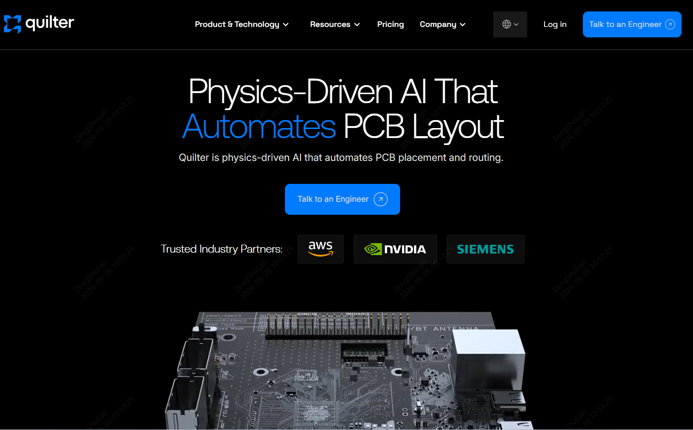
Quilter is a physics-driven AI layout engine that works from an existing schematic. It can be used by hardware teams that want several layout candidates for a finished schematic.
It supports automated placement and routing, then reports the physics and design-rule checks it ran on each design.
- Input: Altium, Cadence, OrCAD, Siemens Xpedition, or KiCad files with board outline, fixed parts, stackup, and rules.
- Output: Layout candidates returned in the native ECAD format.
- PCB workflow stage: Placement and routing.
Key limitation: It does not generate schematics. You must also manually check for length matching, RF routing, and blind or buried vias, as these features are in ongoing development.
3. Cadence Allegro X AI
Allegro X AI is the generative AI layout application in the Cadence Allegro X platform. It is particularly suited to enterprise teams already using constraint-driven design workflows in Allegro X.
It can generate alternative placements, create power and ground planes, and route critical nets within electrical and manufacturing constraints.
- Input: An Allegro X design with its netlist, board outline, and constraint set.
- Output: Placement, plane, and routing results inside Allegro X.
- PCB workflow stage: Layout, with SI and PI analysis through the integrated Sigrity X platform.
Key limitation: It works inside the Cadence environment, so it suits licensed Allegro X teams rather than individual makers.

4. Altium Designer
Altium Designer is a professional EDA platform with AI features documented as part of its Altium 365 cloud environment. It’s a natural fit for teams already using Altium that want to add AI features without changing their existing workflow.
The Engineering Assistant in the Altium 365 Requirements Portal creates, edits, and reviews requirements from natural-language requests.
- Input: Requirements text in Altium 365 and native Altium projects for third-party AI tools.
- Output: Structured requirements; schematic and layout stay in Altium Designer.
- PCB workflow stage: Requirements, with Octopart component data in the design editor.
Key limitation: Altium does not describe its layout automation, such as ActiveRoute, as AI. For AI placement or routing, Altium users export to tools such as Quilter or DeepPCB.

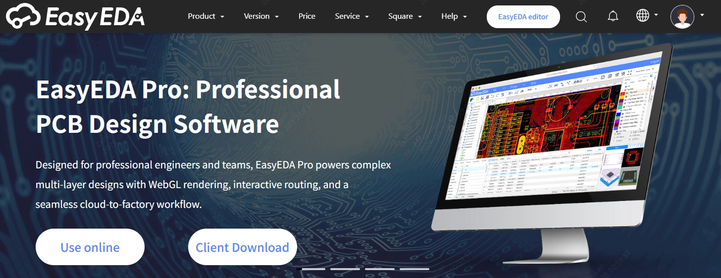
5. EasyEDA Pro
EasyEDA Pro is a free EDA tool that runs in the browser or as a desktop client, and AI connects to it through its Extension API. It is well-suited to makers and small teams looking for a free, native EDA tool with a built-in component library.
EasyEDA's official API skill lets AI coding agents, such as Claude Code, run API commands that edit schematics and PCBs, search the library, and run DRC.
- Input: A native EasyEDA Pro project plus instructions to the connected agent.
- Output: An editable native EasyEDA Pro project and its manufacturing files.
- PCB workflow stage: Schematic, component selection, layout, and DRC can be performed via the commands the agent sends to the API.
Key limitation: Results depend on the connected agent or extension, requiring each change to be verified in the native editor.
Learn more: AI PCB Design: From Prompt to PCB with EasyEDA Pro
6. CELUS
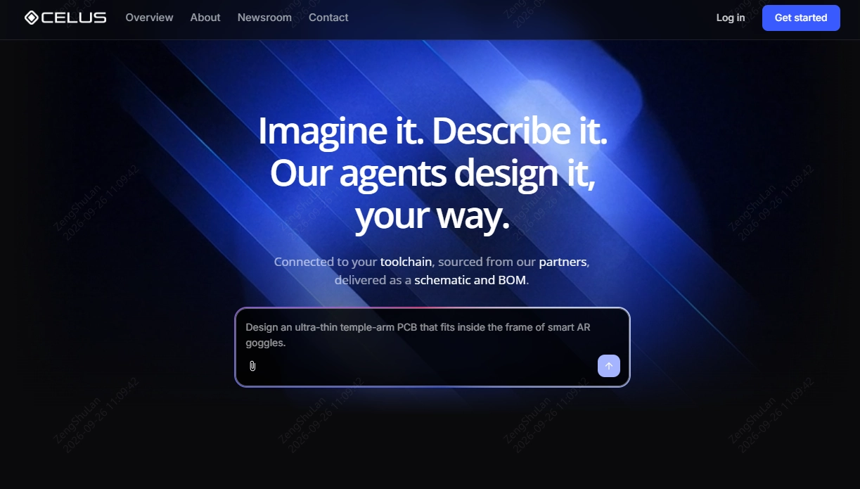
CELUS is a browser-based AI platform that converts requirements into a reference schematic and BOM. It is ideal for engineers who start with requirements and need a sourced BOM early in the process.
It can capture requirements through guided questions, match components and reference designs, generate the schematic, and perform design checks.
- Input: Plain-language requirements.
- Output: A reference schematic and BOM with supply-chain data and alternates, opened in Altium, Cadence, Siemens, Fusion, or KiCad.
- PCB workflow stage: Requirements, component selection, and schematic.
Key limitation: CELUS stops before layout, so placement and routing must be performed in another tool.
7. Circuit Mind
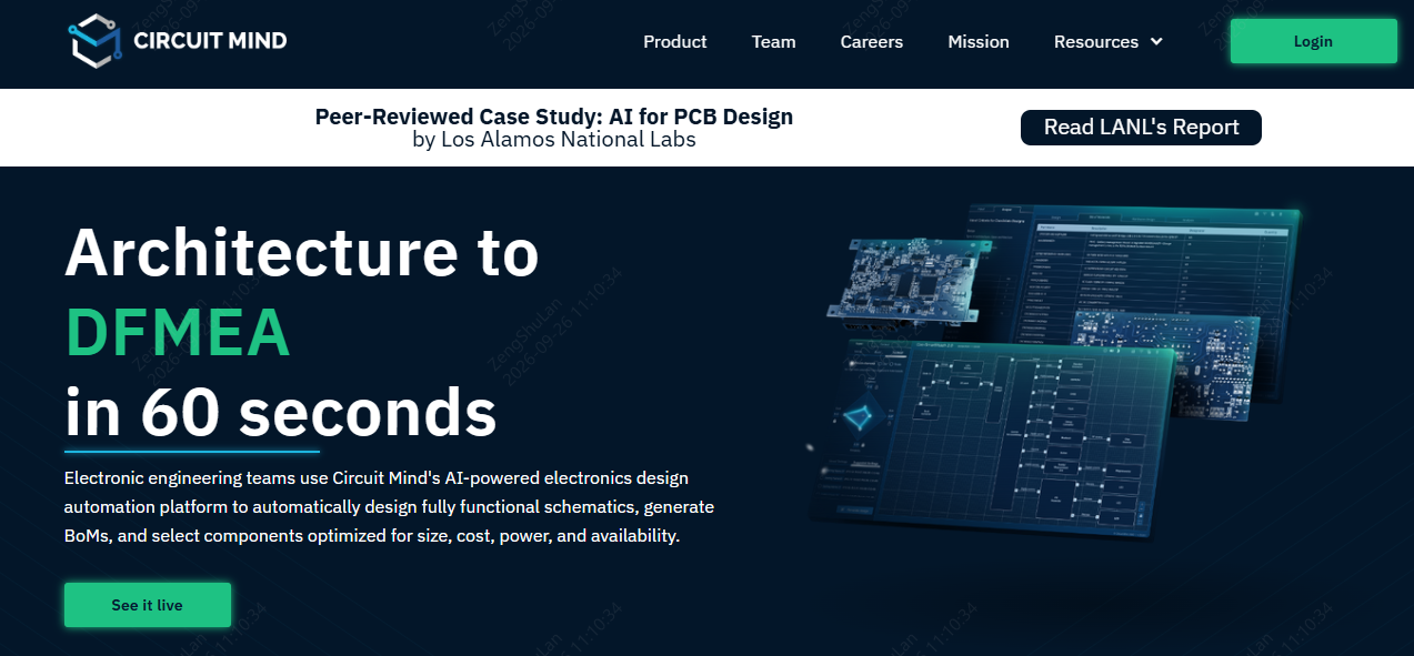
Circuit Mind is an AI design platform that converts a hardware architecture into a schematic and BOM. It is made for professional and enterprise teams that need optimized, documented designs.
This tool searches component combinations against cost, size, power, and availability targets, then generates the schematic and runs verification checks.
- Input: An architecture diagram with functional blocks, signals, and constraints.
- Output: Schematic, BOM, ECAD schematic and library files, plus power, failure-mode (FMEA), and derating reports.
- PCB workflow stage: Architecture, component selection, and schematic.
Key limitation: Its output ends at the schematic and BOM; access starts with a demo and onboarding.
8. DeepPCB
DeepPCB, from InstaDeep, is a cloud AI routing engine trained with reinforcement learning. Designers who route critical nets by hand want the routine routing done quickly.
Its Cooper assistant checks the stackup, net classes, differential pairs, planes, and clearances, and then the engine routes the remaining nets.
- Input: A placed board from Altium, KiCad (via plugin), EasyEDA, Zuken, or other tools through Specctra DSN.
- Output: A routed, DRC-clean board returned to the original design flow.
- PCB workflow stage: Routing.
Key limitation: DeepPCB states that DDR nets, length matching, advanced impedance control, and RF constraints stay with engineers. Self-serve plans cover boards up to 8 layers.

9. JITX
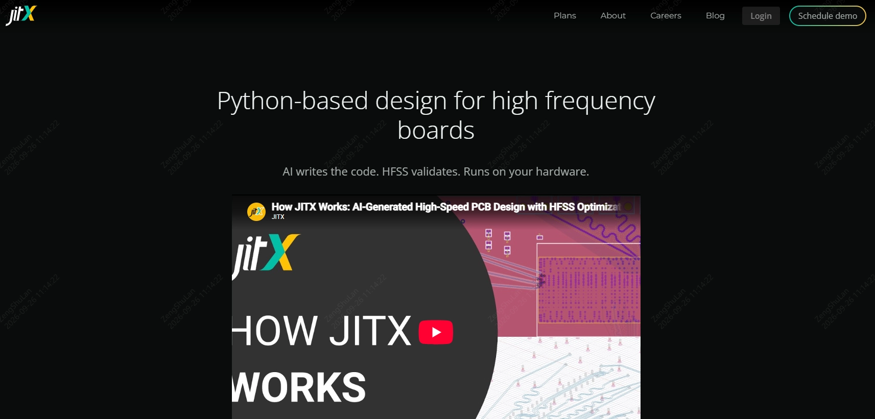
JITX is a code-driven PCB design tool in which requirements and design rules are written in Python. It is ideal for teams with software skills working on high-frequency or reusable designs.
An AI model approved by your organization edits the design code, while JITX generates schematics, board structures, and routing, runs checks, and dispatches HFSS electromagnetic simulations.
- Input: Requirements, stackups, SI targets, and manufacturing rules written in Python.
- Output: Schematics and board layouts, with integrations for KiCad, Altium, and Siemens Xpedition.
- PCB workflow stage: Schematic through layout and SI validation.
Key limitation: It requires Python coding, and the free plan covers only open-source designs.
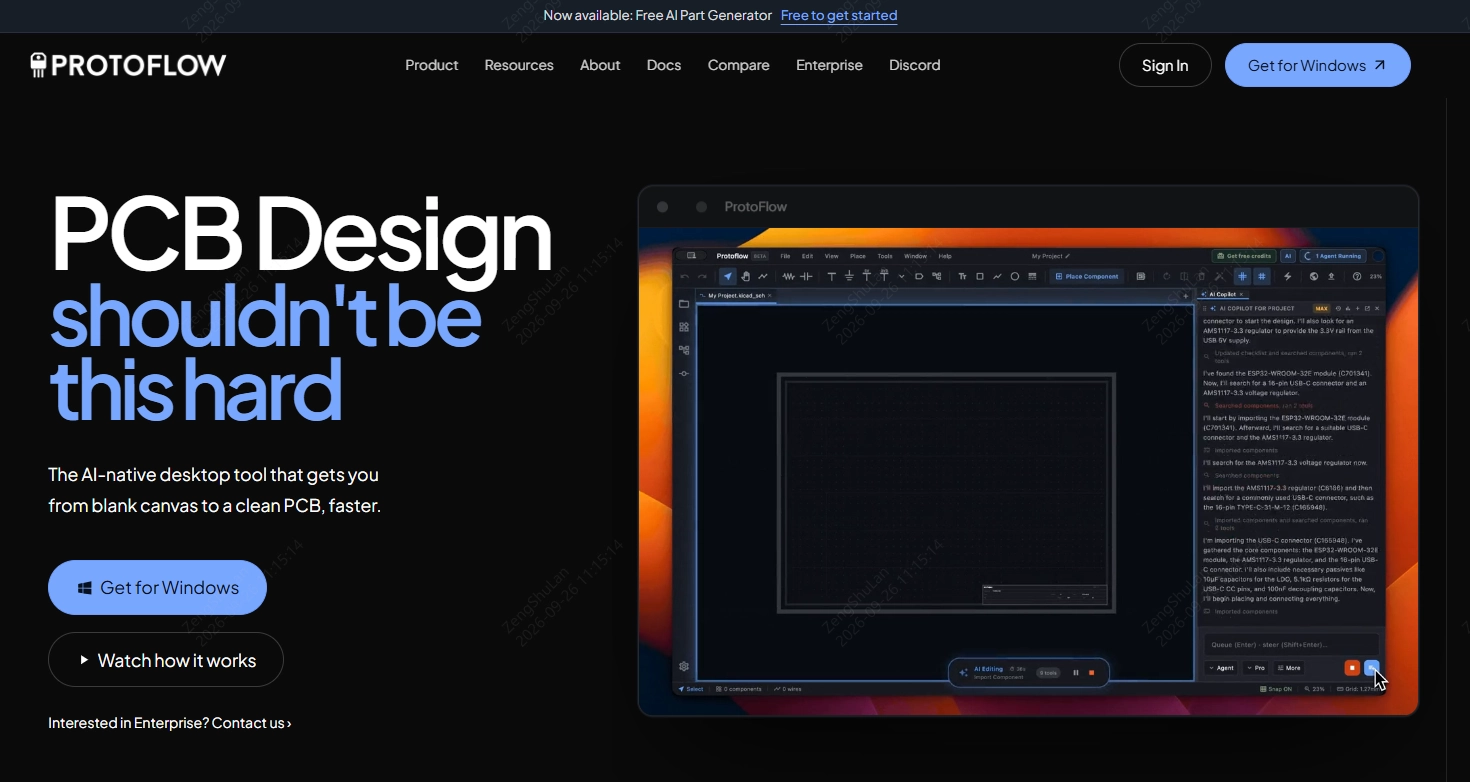
10. ProtoFlow
ProtoFlow is a desktop AI-native EDA tool that turns a plain-language description into a schematic. It is best suited for beginners and makers who want a fast schematic draft to finish in another EDA tool.
It helps to draft the schematic, import real parts from LCSC, DigiKey, and Mouser, and run ERC and DRC on the result.
- Input: A plain-language circuit description.
- Output: An editable project that exports to KiCad, Altium, EAGLE, PADS, or EDIF, plus Gerber and drill files, and BOM and placement files formatted for JLCPCB assembly.
- PCB workflow stage: Schematic and component selection.
Key limitation: ProtoFlow positions itself as a schematic capture tool, so AI placement and routing require another tool. Free AI use has a daily message allowance.
AI PCB Design Tools Compared
In short, requirements tools end at the schematic and BOM, layout engines start from an existing design, and all-in-one tools span every stage.
- A ✓ means the vendor documents AI performing or assisting that stage.
- A — means the stage stays with the engineer or another tool.
| Tool | Schematic | Component Selection | Placement | Routing | Verification | Platform | Best For |
|---|---|---|---|---|---|---|---|
| Flux | ✓ | ✓ | ✓ | ✓ | ✓ | Browser | All-in-one AI workflow |
| Quilter | — | — | ✓ | ✓ | ✓ | Browser | Autonomous layout |
| Cadence Allegro X AI | — | — | ✓ | ✓ | ✓ | Desktop + cloud | Enterprise constraint-driven layout |
| Altium Designer | — | — | — | — | — | Desktop + cloud | Altium teams; AI for requirements |
| EasyEDA Pro + AI agent | ✓ | ✓ | ✓ | ✓ | ✓ | Browser + desktop | Agent-driven design through the API |
| CELUS | ✓ | ✓ | — | — | ✓ | Browser | Requirements to schematic |
| Circuit Mind | ✓ | ✓ | — | — | ✓ | Browser | Architecture to schematic and BOM |
| DeepPCB | — | — | — | ✓ | ✓ | Browser | AI routing of a placed board |
| JITX | ✓ | ✓ | ✓ | ✓ | ✓ | Desktop | Code-driven, high-frequency design |
| ProtoFlow | ✓ | ✓ | — | — | ✓ | Desktop | Prompt to schematic, KiCad handoff |
How to Choose an AI Tool for PCB Design
Choose based on your starting point and EDA software, not on feature count. Identify what you already have, then pick a tool type that accepts that input.
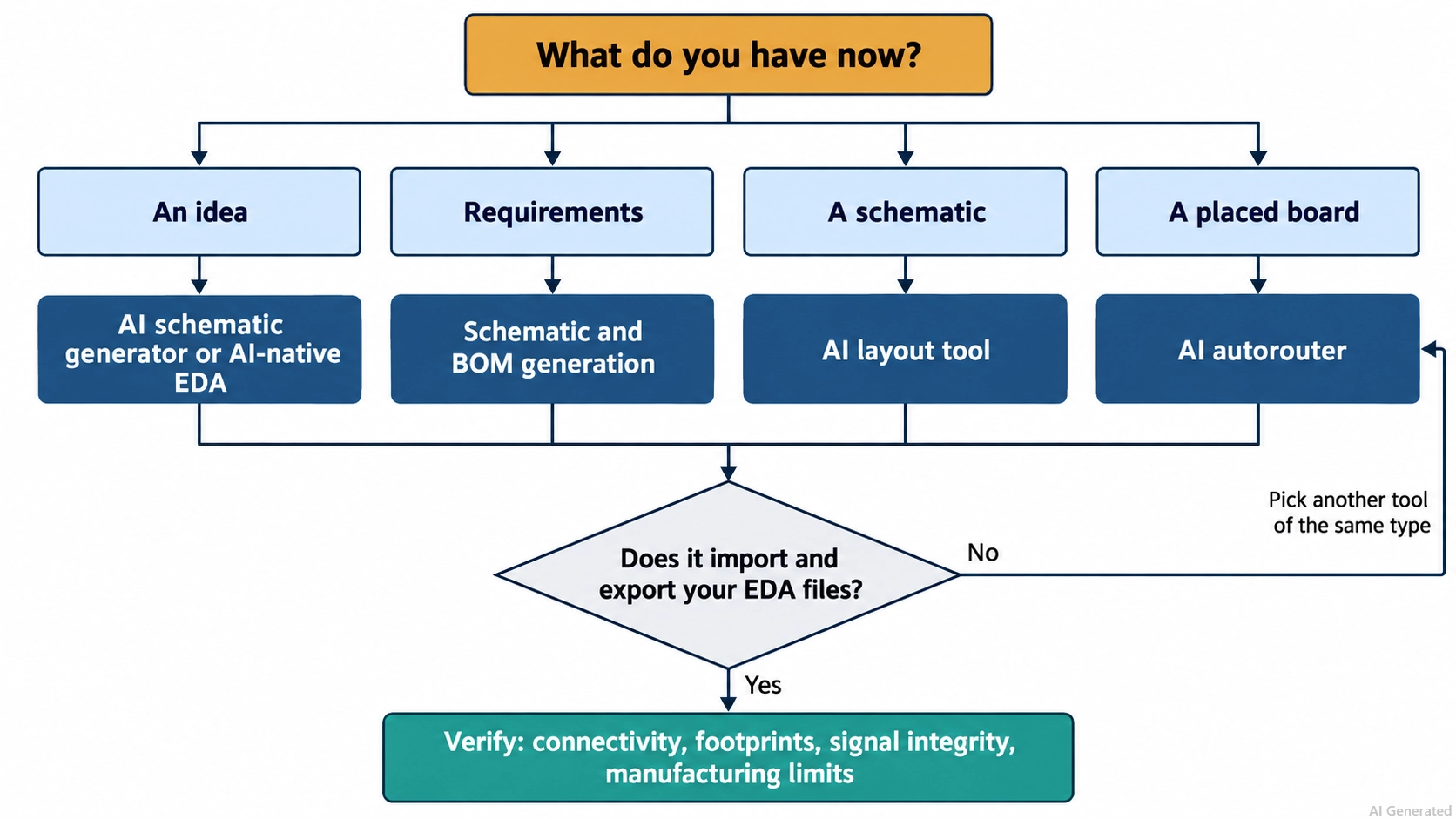
Figure: Decision flow for choosing AI tools for PCB design by starting with the input.
1. If You Are Starting From a Product Idea
Start with a tool that turns design intent into a schematic. The decision comes down to one question: do you need a sourced reference design, or a fast first draft?
- Requirements to schematic and BOM: CELUS and Circuit Mind capture functional blocks and constraints, then return a schematic and BOM for your EDA tool.
- Prompt to schematic: Flux and ProtoFlow draft a schematic from a plain-language description for early exploration.
Once an AI-generated BOM is ready, verify component availability and package information before finalizing the design.
2. If You Already Have a Schematic
Use an AI layout tool that accepts your native design files. Quilter generates placement and routing candidates from Altium, Cadence, OrCAD, Siemens Xpedition, or KiCad files, while Allegro X AI works inside an existing Allegro X project.
Prepare the inputs first: board outline, fixed connector and mounting-hole positions, stackup, net classes, and design rules. Missing rules can produce a layout that looks complete but misses the design intent.
3. If You Need AI Routing
Choose an AI autorouter when placement is already fixed. DeepPCB routes a placed board from Altium, KiCad, or EasyEDA files, and Flux AI Auto-Layout routes a board once placement is finalized in Flux.
Selection rule: route critical nets, such as clocks, high-speed pairs, and RF paths, by hand first, then let the AI route the rest. DeepPCB and Quilter both describe this pre-routing approach.
4. If You Use KiCad
KiCad 10 does not include a built-in AI assistant, so AI enters through tools that read and write KiCad files. Quilter, DeepPCB (through a plugin), CELUS, ProtoFlow, and JITX support KiCad import or export.
General-purpose AI agents can also operate the KiCad interface directly as computer-use agents. The GPT-6 Astra PCB design project in KiCad demonstrates this approach, including the verification still required.
5. If You Use EasyEDA Pro
Choose the stage you want to automate. For schematic and PCB edits, connect an AI coding agent through EasyEDA's official API skill. For AI routing, send the placed board to DeepPCB, which accepts EasyEDA Pro files.
Keep the native project as the source of truth, and run DRC in EasyEDA Pro after each agent change.
6. If You Need Professional High-Speed PCB Design
Use constraint-driven EDA with AI, and keep your design constraints as the source of truth. Allegro X AI routes critical nets within the Allegro X constraint system, with SI and PI analysis through Sigrity X. JITX encodes SI targets and stackups in code, with HFSS simulation in the loop.
Before trusting an AI layout on a high-speed board, confirm how the tool handles:
- Impedance: Controlled-impedance traces calculated from the actual stackup.
- Differential pairs and length matching: Pair routing with length and skew tuning.
- SI and PI: Crosstalk, return paths, and power delivery.
- HDI and thermal: Microvia structures, copper balance, and heat paths.
- Manufacturing constraints: Your fabricator's trace, space, drill, and stackup limits.
| Your Situation | Relevant Tool Type | Examples |
|---|---|---|
| I only have an idea | AI schematic or architecture tool | Flux, ProtoFlow |
| I have requirements | Schematic and BOM generation | CELUS, Circuit Mind |
| I already have a schematic | AI placement and routing | Quilter, Cadence Allegro X AI |
| I need an autonomous layout | AI layout engine or autorouter | Quilter, DeepPCB |
| I use KiCad | KiCad-compatible AI tools | Quilter, DeepPCB, CELUS, ProtoFlow, JITX |
| I use Altium | Altium-compatible AI tools | Quilter, DeepPCB, CELUS, JITX |
| I want a browser-based design | Cloud AI EDA | Flux, EasyEDA Pro |
| I want free tools | Free and open-source options | ProtoFlow, Quilter for eligible users, JITX for open-source designs |
Once the AI tool completes placement and routing, proceed to PCB assembly to build a prototype and verify the board's performance before moving to volume production.
What Are the Limitations of AI PCB Design Tools?
AI tools speed up drafting, placement, and routing, but their output can still contain errors in connectivity, footprint, signal integrity, and manufacturability. An engineer must check and sign off on each one manually before placing a PCB/PCBA order.
1. AI Can Make Connectivity or Component Errors
AI tools can connect the wrong pins, leave nets unconnected, or select parts with the wrong rating or package. Altium's AI notice states that "AI-generated content may be incomplete or incorrect" and that qualified engineers must review every output.
Check the netlist against each datasheet pin by pin, and confirm each part's voltage, current, and package against the design requirements.
2. Generated Footprints Still Need Verification
A footprint can look correct in the PCB editor and still cause problems during assembly. In the GPT-6 Astra EasyEDA Pro project, the first native check reported 50 association mismatches due to distinct footprints sharing the same library name.
Check each generated or imported footprint against the manufacturer's recommended land pattern:
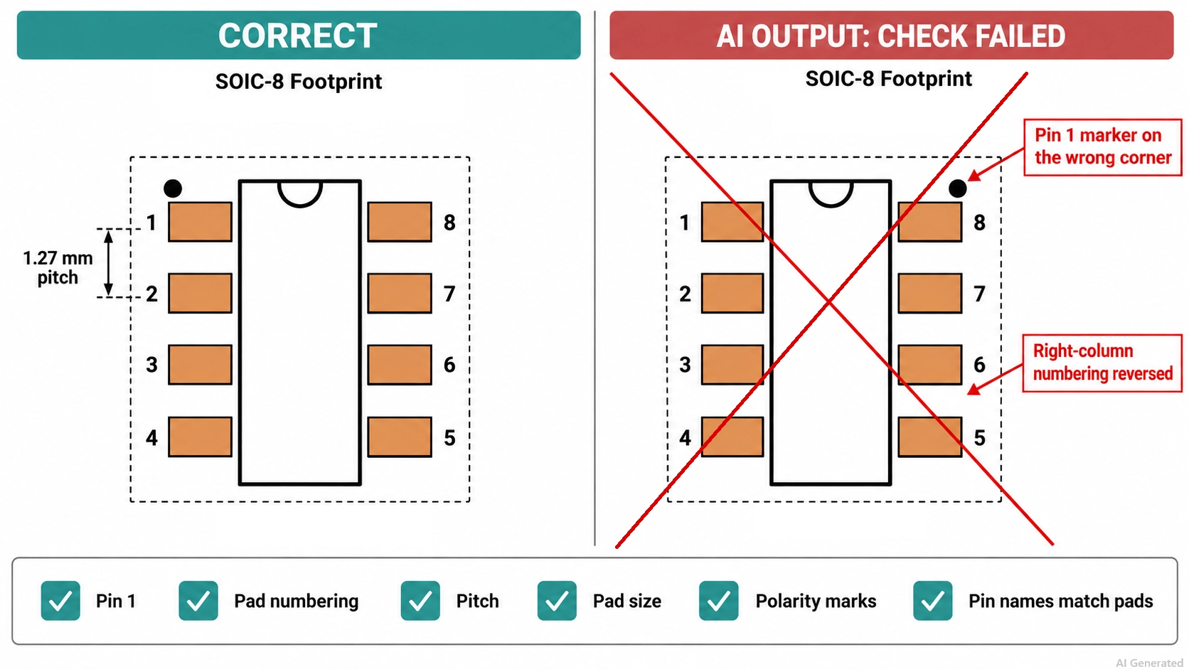
Figure: Checking an AI-generated footprint for pin 1, pad numbering, and pitch.
- Pin 1 location and pad numbering
- Pad size, pitch, and courtyard
- Polarity and orientation marks
- Schematic PINs mapped to the correct footprint pads
3. AI Routing Does Not Replace Signal Integrity Analysis
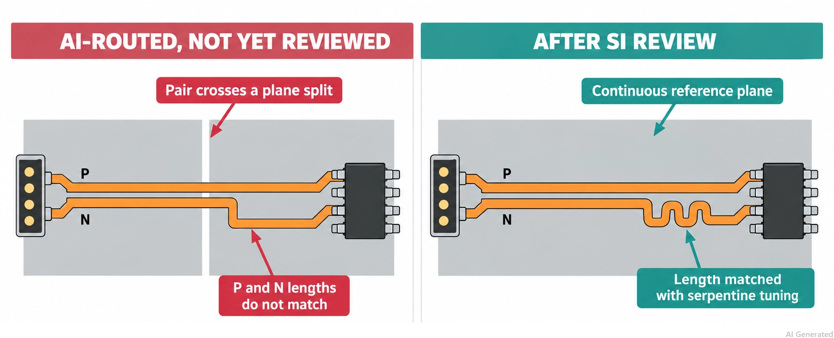
Figure: AI-routed differential pair checked for reference-plane continuity and length matching.
A fully routed, DRC-clean board confirms geometry, not electrical performance. DeepPCB, for example, leaves DDR nets, length matching, advanced impedance control, and RF constraints to engineers.
For high-speed nets, check impedance against the real stackup, reference-plane continuity under each pair, length matching, skew, and crosstalk. Run SI and PI simulations where the design requires it.
4. Manufacturing Constraints Still Matter
A clean DRC confirms that the design meets the rules you entered, but those rules may not fully reflect your fabricator’s capabilities. A board can therefore pass DRC and still present manufacturing challenges.
Before ordering, check minimum trace and space, drill sizes, annular ring, solder mask openings, and the stackup against the manufacturer's published limits. Also, confirm assembly needs, such as component spacing and fiducials.
5. Human Engineering Review Is Still Required
An engineer still owns the decisions that need accountable sign-off: the architecture, the trade-offs, compliance, and the final release. Review the AI output using the same schematic review, layout review, and prototype testing as for any new design.
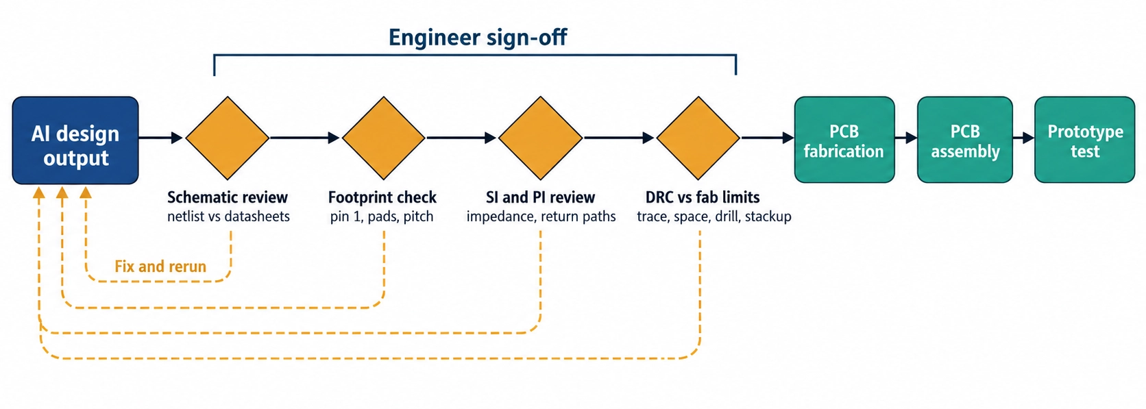
Figure: Engineering review checkpoints between AI design output and PCB fabrication.
AI can accelerate the design process, but engineering verification remains an essential part of the workflow.
And once your design passes review, upload your Gerber, BOM, and CPL (pick-and-place) files to get an instant quote for PCB fabrication and assembly in one order.
Conclusion
AI tools for PCB design now cover different parts of the workflow: some help turn requirements into schematics and BOMs, others focus on placement and routing, and some combine several stages within a single environment.
The right choice depends largely on where you are starting. Whether you have an idea, a set of requirements, a schematic, or a partially placed board, look for a tool that fits that stage and works with your existing EDA workflow. AI can reduce repetitive work and speed up iteration, but the final design still needs engineering review.
The most useful AI tool is not necessarily the one that does the most. It is the one that fits your workflow and provides the right level of automation without taking control away from the engineer.
FAQs About AI Tools for PCB Design
Q: Can ChatGPT Design a PCB?
Not on its own. A general-purpose model can draft a circuit or operate EDA software through an agent, but the board still needs EDA tools, datasheet checks, and engineering review.
Q: Is There a Free AI Tool for PCB Design?
Yes, with limits. ProtoFlow has a free plan with a daily AI allowance, JITX is free for open-source designs, and Quilter is free for eligible academic, personal, and small-team use.
Q: Which AI PCB Design Tool Is Best for Beginners?
Usually, a tool with a guided, prompt-based workflow, such as Flux or ProtoFlow. The AI drafts the schematic and runs error checks while you learn to verify the result.
Q: Does KiCad Have Built-In AI?
No. KiCad 10 does not include a built-in AI assistant. AI interacts with KiCad via tools that import or export KiCad files, such as Quilter and DeepPCB, or through external agents.
Q: Will AI Replace PCB Designers?
Not at present. Current tools automate drafting, placement, and routing, but engineers still define constraints, review footprints and signal integrity, and sign off on the design for manufacturing.
Popular Articles
• AI Tools for PCB Design: Which Tool Fits Your Workflow Stage?
• AI PCB Design: From Prompt to PCB with EasyEDA Pro
• GPT-6 Astra PCB Design in KiCad: From Brief to Verified Native Project
• GPT-6 Astra PCB Design in EasyEDA Pro: What Worked, What Failed, and What We Learned
• How to Design Your Own Keyboard PCB: From Layout to Firmware
Keep Learning
Mastering PCB Design Rules: A Comprehensive Guide for Optimal Results
Key Takeaways Follow core PCB design rules for reliable electrical and mechanical performance. Optimize trace width, spacing, impedance, and vias for signal integrity and manufacturability. Apply DFM and DRC early to identify potential manufacturing and layout issues. Consider thermal management, grounding, and testing during the PCB design stage. Align design rules with your PCB manufacturer’s capabilities to improve production reliability and reduce redesigns. PCB design rules are essential guidelin......
KiCad MCP: How to Design a PCB with Claude Code [Step-by-Step]
Key Takeaways Claude can design PCBs in KiCad: By connecting Claude to KiCad through an MCP server, you can use AI to create and modify PCB designs. In this project, Claude helped turn a 5 A XL4015 buck converter netlist into a two-layer, 63 × 33 mm PCB layout with zero ERC violations and zero DRC errors after minor initial fixes. Set up Claude securely: Use a KiCad MCP server that starts in read-only mode. Review the server code before installing it, connect through stdio, and allow editing only in a......
Claude Code PCB Design: Can It Build a Real Board in EasyEDA Pro?
Key Takeaways Claude Code PCB design: Using Claude Opus 5.5 and EasyEDA Pro 3.2.149, I converted a 47-component, three-page schematic from a PDF into a fully routed, two-layer PCB with zero DRC errors. EasyEDA Pro integration: The EasyEDA API skill connects Claude Code to EasyEDA Pro through a local bridge server and the Run API Gateway extension. This allows Claude to control the editor via JavaScript, with a 30-second timeout per API call. Design verification: A successful API response doesn't alway......
How to Design a PCB with Flux.ai (Step-by-Step Guide)
Key Takeaways This step-by-step Flux PCB design tutorial demonstrates the complete workflow by creating a compact 15 × 15 mm USB 2.0 hub, refining the layout, routing high-speed differential traces, and preparing manufacturing files for JLCPCB PCB fabrication and assembly. We are all hearing news; new AI models are being released every month. And it has finally reached the schematic editor. Flux.ai is a browser-based AI PCB design tool with a built-in AI agent that behaves like a junior hardware engin......
AI Tools for PCB Design: Which Tool Fits Your Workflow Stage?
AI tools can now assist with PCB architecture, schematic generation, component selection, placement, routing, and design verification. However, different tools target different stages of the PCB workflow. This guide compares AI tools for PCB design based on what they actually do, what inputs they require, and where they fit within a real engineering workflow. In this guide, you will learn: The 6 types of AI PCB tools and the input each one needs What AI PCB design tools do, compared stage by stage How......
AI PCB Design: From Prompt to PCB with EasyEDA Pro
Key Takeaways AI PCB design uses AI agents to automate schematic creation, component selection, layout, and verification inside a real EDA editor — not just generate images. The workflow connects EasyEDA Pro to an AI coding agent (Claude Code or Codex) through the EasyEDA API Gateway, the open-source API Skill, and a local bridge server. Setup takes about ten minutes and is fully local-first: designs, API calls, and intermediate code never leave your machine. Because the agent places real library part......