
How To Export BOM and Pick & Place Files From KiCad 10 [2026 Updated]
Last updated on Jul 15, 2026
When you place an SMT Assembly order on JLCPCB, two files do the heavy lifting: the BOM (Bill of Materials), which tells JLCPCB which parts to place, and the CPL / Centroid file, which tells the machine where and how to place them.
Note: Applicable Versions
This guide was written and verified on KiCad 10.0.3 (current stable release). The same workflow applies to KiCad 9 and KiCad 8, only some toolbar icons and menu labels differ slightly in the UI.
What you'll need
- KiCad 10 installed (download from the official KiCad website).
- A completed schematic and a routed PCB for your design.
- A JLCPCB account, to upload the files when you place the SMT order.
The two files JLCPCB needs for assembly order
1. The BOM (Bill of Materials)
The BOM file is required to be a .csv, .xls or .xlsx file that has, at least, these fields: Comment (e.g. 10k, 470uF), Designator (e.g. R1, C2), Footprint (e.g. 0805, 1206) and the JLCPCB / LCSC Part #.
JLCPCB has released the sample BOM that you can use as a template:
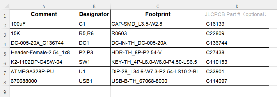
JLCPCB's official sample BOM
2. The CPL / Centroid file (Pick & Place)
Centroid, CPL and Pick & Place are three names for the same file. It gives the X/Y location, rotation and board side of every component so the assembly machine knows where to drop each part.
JLCPCB expects these columns: Designator, Mid X, Mid Y, Rotation and Layer. Coordinates should be in millimetres.
Two Methods to Generate the Files
KiCad 10 can generate both files with its own integrated tools (Method 1), the output format is based on KiCad's own column names, and some slight formatting is required to make it compatible with JLCPCB.
The second one is the free JLCPCB Fabrication Toolkit plugin (Method 2) that makes it possible to export Gerbers, BOM and CPL directly in JLCPCB's format with a single click.
Note
Just if you are short on time? Jump to Method 2 (Fabrication Toolkit) as it is the recommended path for JLCPCB orders because the BOM and CPL come out JLCPCB-ready with no manual editing.
Our example project
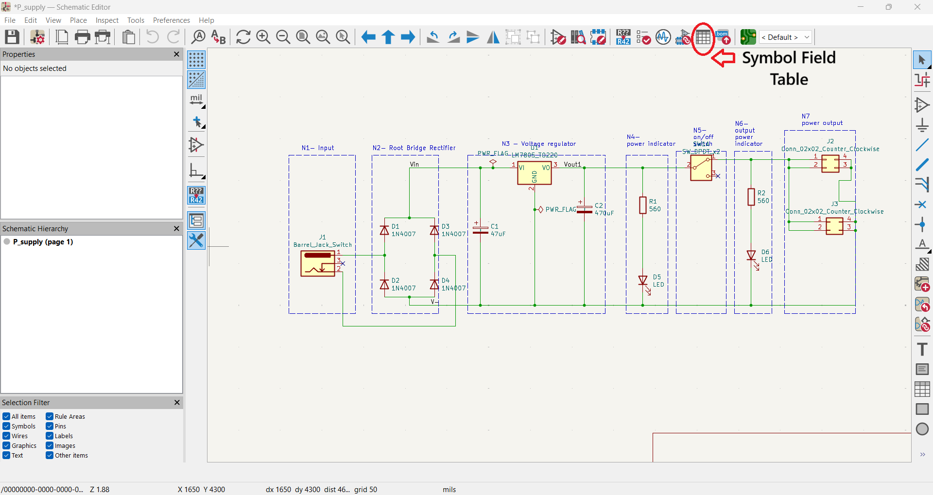
To keep things concrete, the screenshots below use a simple breadboard power supply (bridge rectifier + LM7805 regulator with power-indicator LEDs). Here is its schematic and routed PCB.
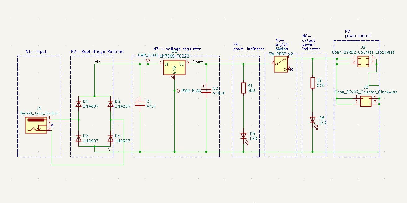
Example schematic - breadboard power supply.
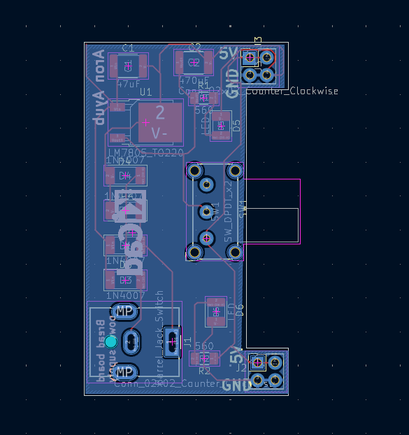
Example PCB layout for the same design.
Method 1: KiCad's built-in export
Step 1: Open the Symbol Fields Table
In the Schematic Editor, open Tools → Edit Symbol Fields Table, or click the Symbol Fields Table button on the top toolbar. This is where KiCad 10 generates the BOM.
KiCad 10 also keeps a quick .bom export button on the toolbar (shown below). Both routes open the same Symbol Fields Table dialog used for the BOM.
The quick “.bom” export button in the Schematic Editor toolbar.
Step 2: Add an LCSC Part # field
Schematic Editor - the Symbol Fields Table button on the top toolbar.
By default the table has no column for the JLCPCB/LCSC part number. Click the (Add Field) button on the left and create a field named LCSC Part #. JLCPCB uses this to match each component to its parts library.
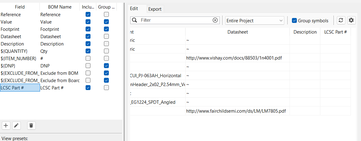
Adding a new field in the Symbol Fields Table (name it “LCSC Part #”).
You can type values straight into the table, or set them per component. Either though symbol field table or by Double-click a symbol in the schematic to open Symbol Properties and enter its LCSC Part # (and check the value/footprint).
Step 3: Export the BOM as CSV
Switch to the Export tab of the Symbol Fields Table. Set Format presets to CSV, confirm the field delimiter is a comma, set the output file name, then click Export.
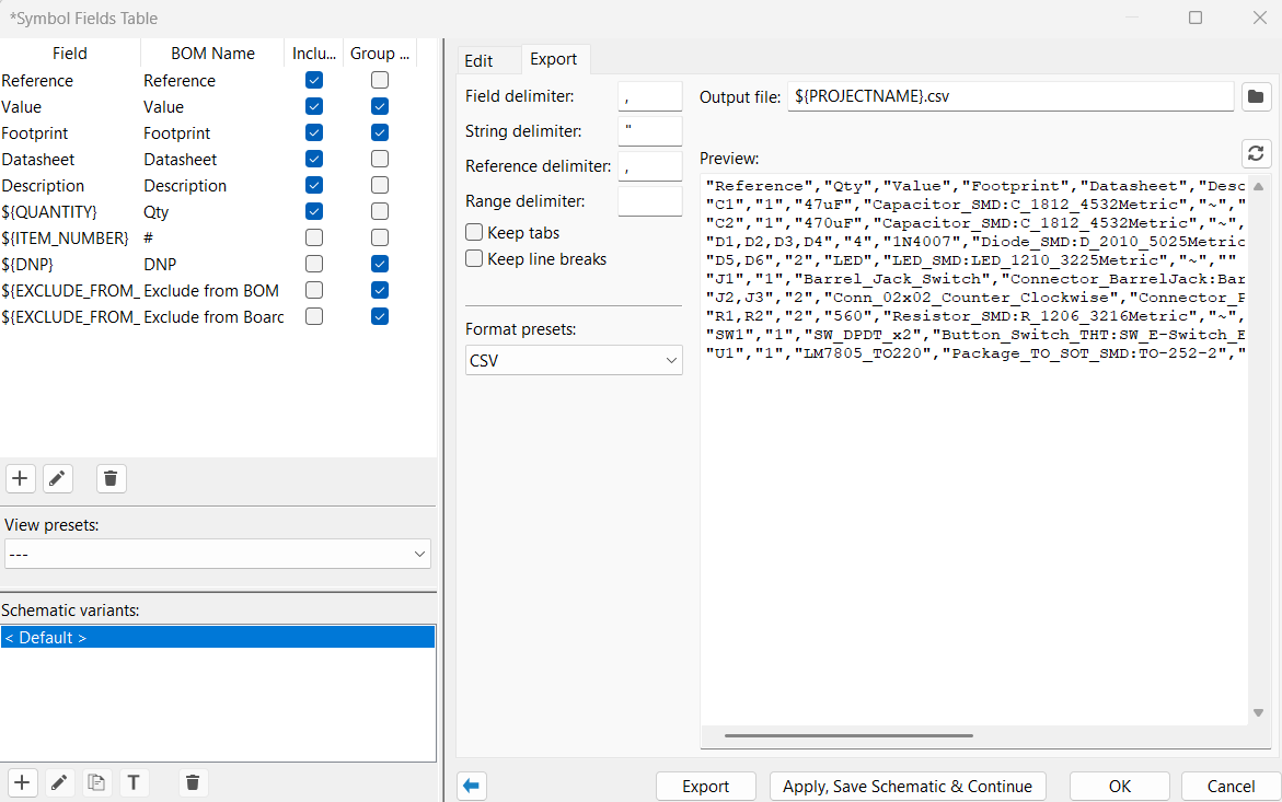
Symbol Fields Table → Export tab: choose the CSV preset and export.
Step 4: Review the exported BOM
The exported CSV looks like the file below - with KiCad's default headers: Reference, Qty, Value, Footprint, Datasheet, Description.
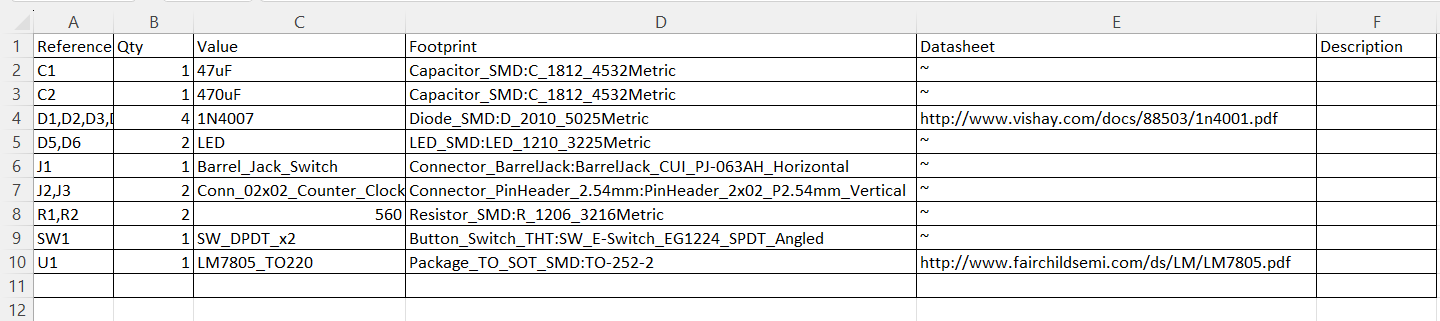
The BOM is exported by KiCad's built-in tool (default KiCad headers).
These headers do not match JLCPCB's sample BOM. Before uploading you must rename/rearrange the columns to Comment, Designator, Footprint, JLCPCB Part # (e.g. Reference → Designator, Value → Comment) in Excel or skip the editing entirely by using Method 2.
Step 5: Generating the Centroid (CPL) file with built-in tools
For the placement file, open the PCB Editor and go to File → Fabrication Outputs → Component Placement (.pos). Export as CSV, with units set to millimetres and a single file for both sides.
KiCad writes headers Ref, PosX, PosY, Rot, Side, which you then rename to Designator, Mid X, Mid Y, Rotation, Layer for JLCPCB.
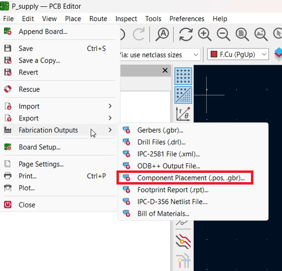
The CPL is exported by KiCad's built-in tool.
Method 2: JLCPCB Fabrication Toolkit (recommended)
The Fabrication Toolkit by bennymeg is a free KiCad plugin that exports the Gerbers, the BOM and the CPL all in JLCPCB's required format just in one click.
Step 1: Open the Plugin and Content Manager
From the KiCad Project Manager home screen, open the Plugin and Content Manager.
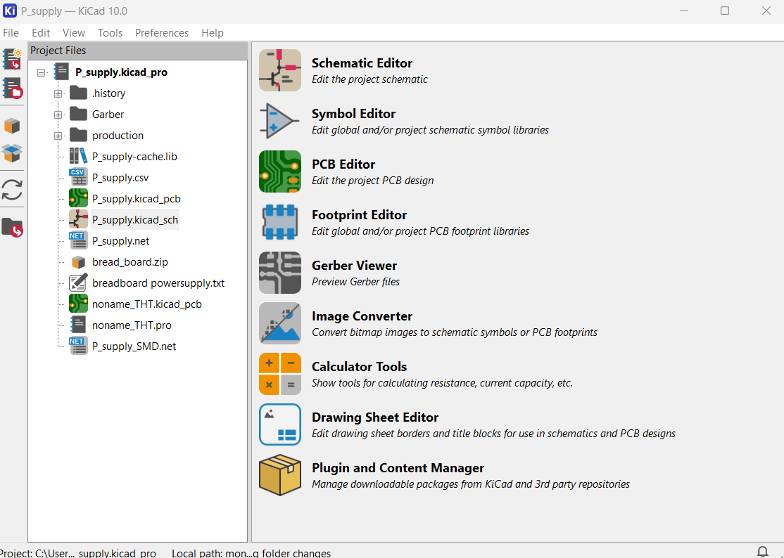
KiCad 10 Project Manager
Step 2: Install the Fabrication Toolkit
In the manager, search for Fabrication Toolkit, click Install, then click Apply Pending Changes at the bottom.
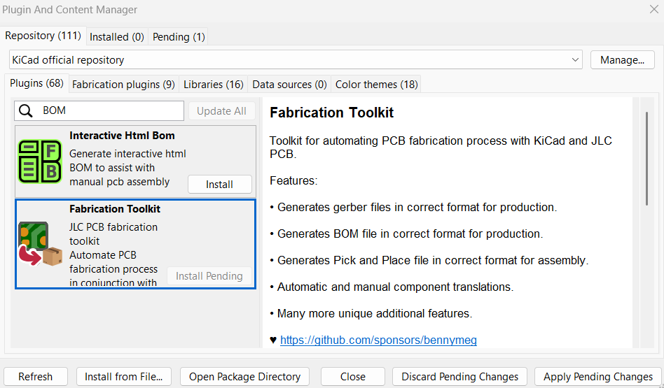
Find “Fabrication Toolkit”, click Install, then Apply Pending Changes.
Step 3: Run the toolkit from the PCB Editor
Open your board in the PCB Editor. A new Fabrication Toolkit button appears on the top toolbar just click it.
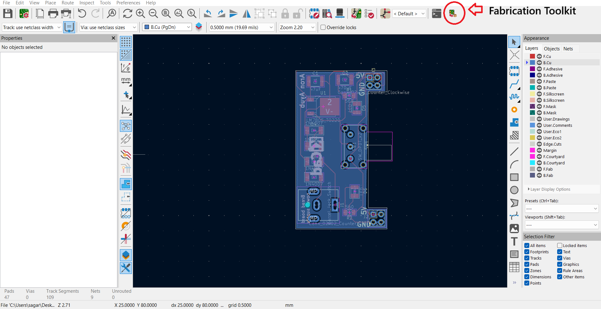
The Fabrication Toolkit button in the PCB Editor toolbar.
Step 4: Fill in the part data
You can type values straight into the table, or set them per component. Double-click a symbol in the schematic to open Symbol Properties and enter its LCSC Part # (and check the value/footprint).
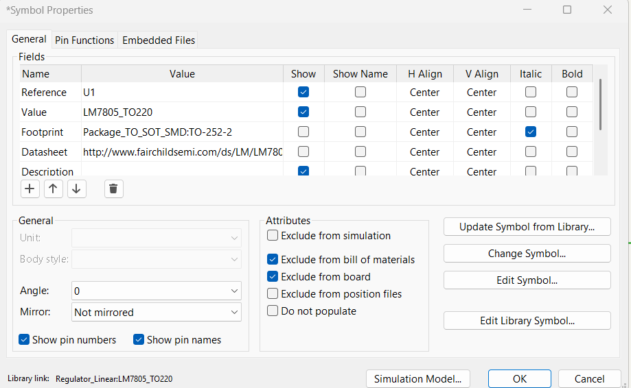
Symbol Properties (double-click a symbol) — add the LCSC Part # field value here.
The same idea applies on the board: double-click a footprint in the PCB Editor to open Footprint Properties, where you can confirm the footprint and fabrication attributes.
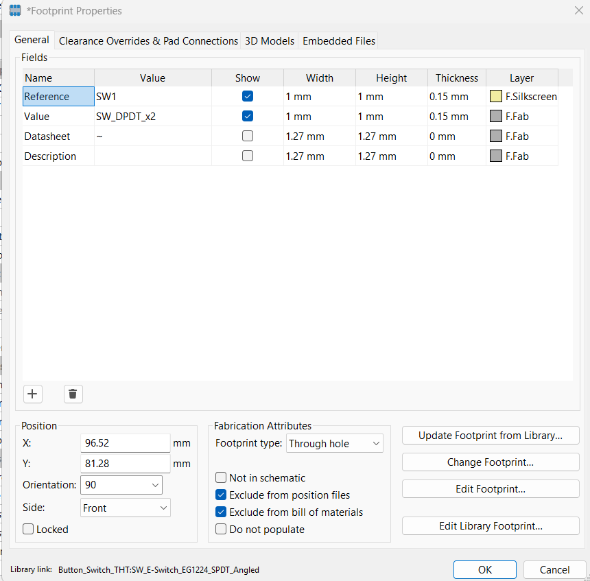
Footprint Properties (double-click a footprint in the PCB Editor).
Step 5: Configure the options and Generate
Keep Apply automatic component translations ticked (this fixes part rotations/positions for JLCPCB) and Apply automatic fill for all zones if you use copper pours. Leave the archive name blank to use the defaults, then click Generate.
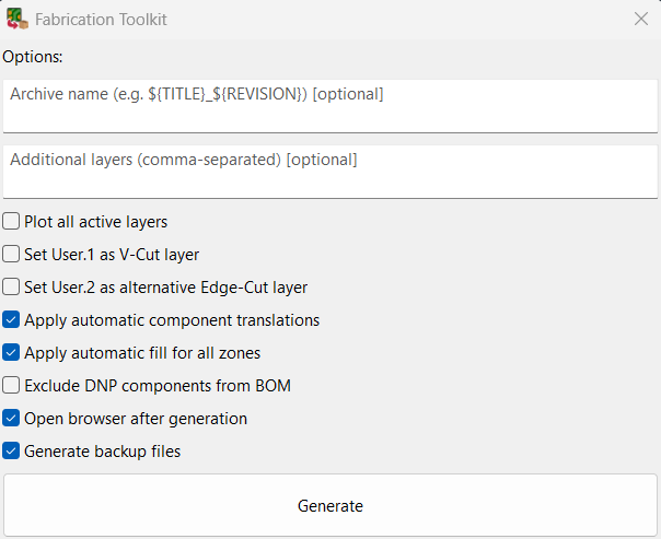
Fabrication Toolkit options — click Generate.
Step 6: Find your production files
The plugin creates a production folder next to your project containing everything you need: the Gerber .zip, bom.csv, positions.csv (the CPL), the designators list and an IPC netlist.
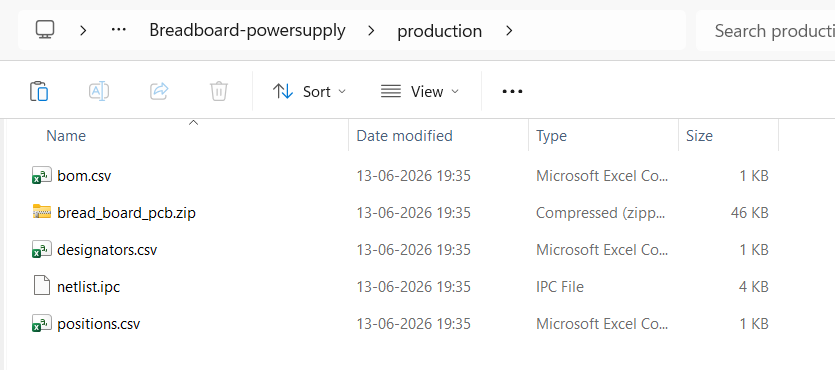
The production folder generated by the toolkit (Gerbers, BOM and CPL together).
The generated BOM
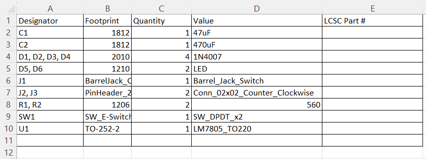
Open bom.csv. Its columns are Designator, Footprint, Quantity, Value, LCSC Part # already aligned with JLCPCB's sample BOM, so no reformatting is needed.
bom.csv from the Fabrication Toolkit
The generated CPL (Centroid / Pick & Place)
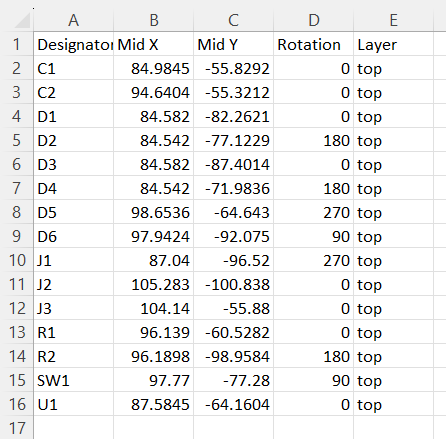
Open positions.csv this is your centroid / CPL / Pick & Place file. Its columns are Designator, Mid X, Mid Y, Rotation, Layer in millimetres and exactly the format JLCPCB expects, with no header editing.
positions.csv : the CPL / centroid / Pick & Place file from the Fabrication Toolkit
Uploading your BOM and CPL to JLCPCB
Step 1: Upload the two files
On the JLCPCB SMT Assembly quote page, upload bom.csv to the BOM slot and positions.csv to the CPL slot, then click Process BOM & CPL.
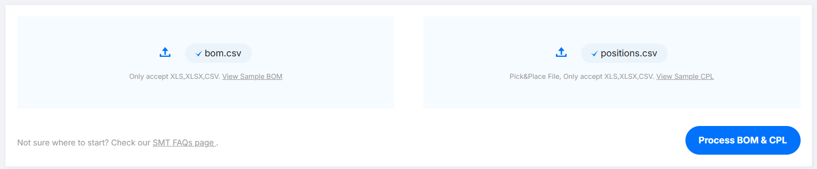
Uploading bom.csv and positions.csv on JLCPCB, then Process BOM & CPL.
Step 2: Review the matched parts
JLCPCB automatically matches your components to its parts library and shows how many parts are detected, confirmed and not yet selected.
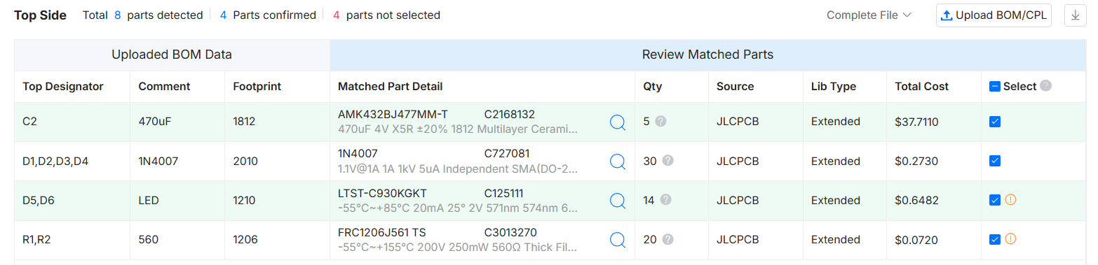
JLCPCB's BOM review
Step 3: Select any unmatched parts
For any component JLCPCB could not match (often because the LCSC Part # was blank), click into the row and use Search Parts to choose a suitable part from stock.
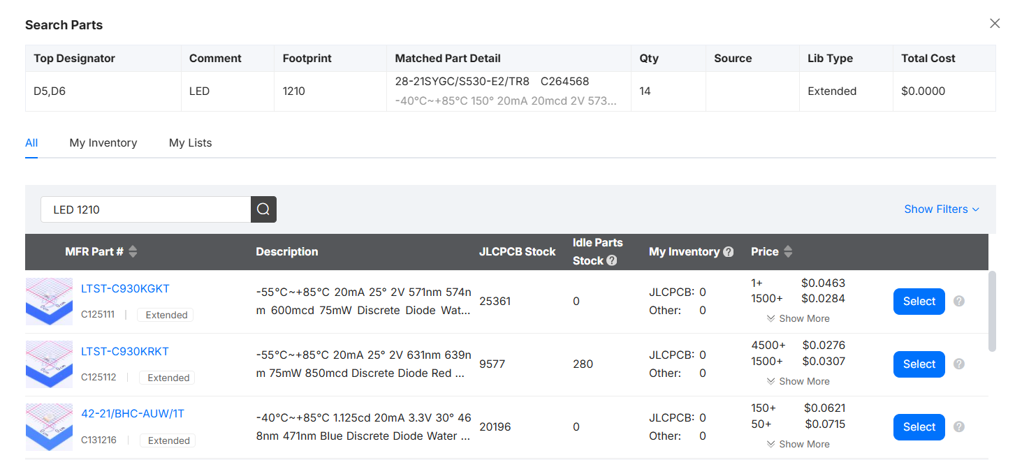
JLCPCB's Search Parts dialog for selecting an unmatched component.
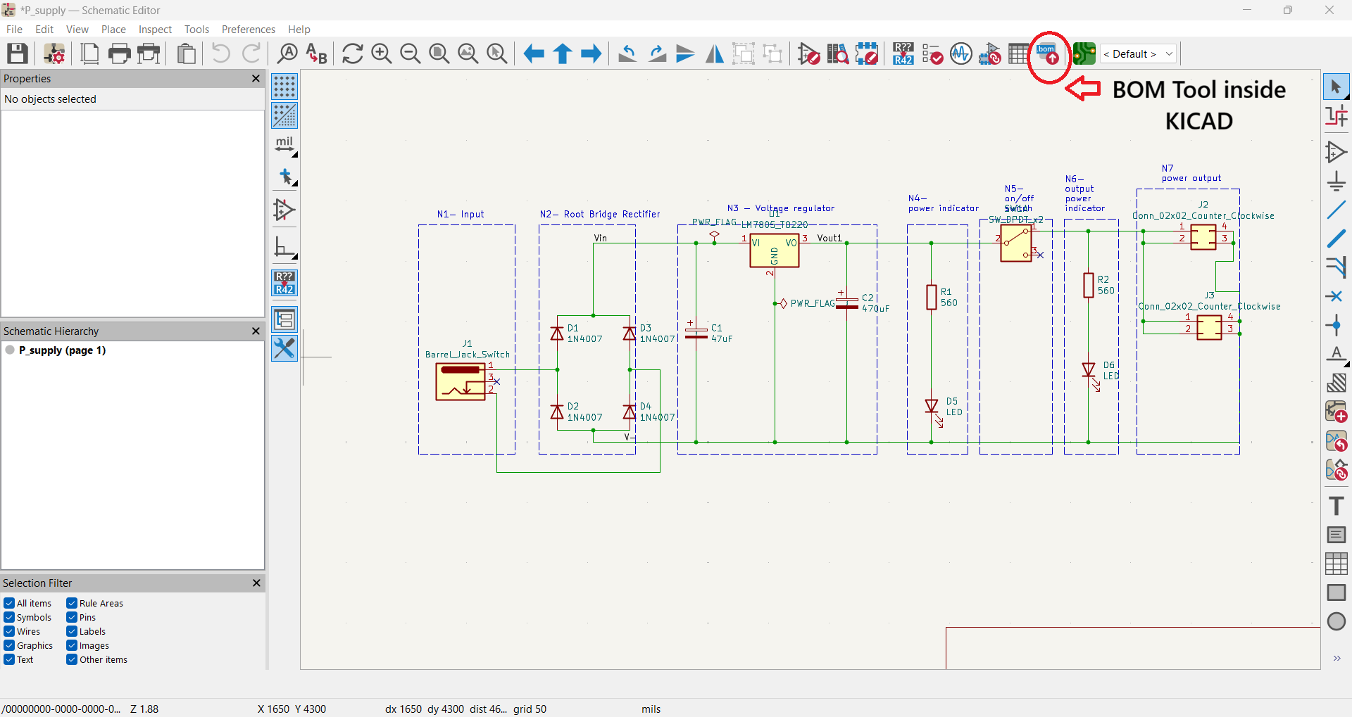
To fill LCSC part numbers while designing, browse the JLCPCB Parts Library / BOM Tool and copy the component number (e.g. C125111) into the LCSC Part # field of each symbol.
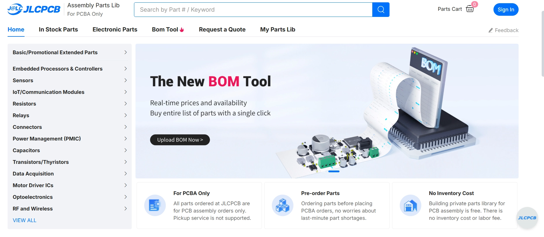
JLCPCB BOM Tool for easy BOM preparation