
From Concept to Production : How PCB DFM Guidelines and Analysis Ensure Smooth Manufacturing Transitions
10 min
- The Bridge Between PCB Design and Manufacturing: DFM Fundamentals
- Essential PCB DFM Guidelines Every Designer Should Know
- Performing Effective PCB DFM Analysis
- Transforming Designs with DFM-Driven Improvements
- Best Strategies for Incorporating DFM Early
- Frequently Asked Questions (FAQ)
When designing a product for a mass audience, it is better to test it thoroughly before deploying it to the market. Because the research and development of the product is quite expensive and time-consuming. Designing a PCB that works on your desk is one thing. Once the design is finalised, the PCB is manufactured and assembled repeatedly without any drama. This is where PCB Design for Manufacturing (DFM) quietly saves projects and engineering reputations.
Many PCB issues don't come from bad schematics or poor routing. But from the designs that are technically correct on paper but practically unbuildable. DFM acts as the translator between design intent and manufacturing reality. We can test different approaches to design a hardware in the prototype phase, but when making for a mass audience, companies are strict on only one final design. PCB DFM guidelines and analysis ensure that the transition from concept to production is smooth and cost-effective. In this article, we will see DFM in depth through some practical examples. Sometimes it is just a game of humour.
The Bridge Between PCB Design and Manufacturing: DFM Fundamentals
Defining DFM and Its Place in the Development Cycle
Design for Manufacturing (DFM) refers to a structured set of rules and checks that are used to ensure that a PCB is fabricated and assembled with high yield. In simpler terms, DFM answers the question: “Can this board actually be built without causing pain to the manufacturer?” DFM is not about creativity; it is about predictability. In the DFM rules, there are considerations for fabrication tolerances, drill accuracy, copper etching limits, soldering behaviour, and assembly constraints. A design that ignores DFM may still function electrically, but it often results in:
- Low manufacturing yield
- Unexpected production delays
- Higher per-board cost
- Assembly failures and rework
DFM belongs early in the development cycle. Ideally, we do the DFM checks right after the layout is finalised. Treating DFM as a final checklist is like checking seatbelts after the crash.
Evolution from Basic Rules to Comprehensive Analysis Tools
In the early days of PCB design, Design for Manufacturing was largely a rule-of-thumb exercise. It is often summarised as a short list of don’ts. Designers were warned not to make traces too thin, not to place vias too close together, and not to shrink pads beyond safe limits. These guidelines were typically based on past failures and the manufacturing experience of the designer and fabricator. This approach worked to some extent because it was well tested but relied heavily on individual expertise. Modern PCB DFM analysis has evolved far beyond these basic constraints. Nowadays, the process falls into a data-driven and highly automated region. Today’s DFM tools can automatically analyse Gerber and drill files, flag out the potential fabrication and assembly risks. It can simulate soldering defects and compare designs against manufacturer-specific rulesets.
Essential PCB DFM Guidelines Every Designer Should Know
Trace Width, Spacing, and Annular Ring Standards
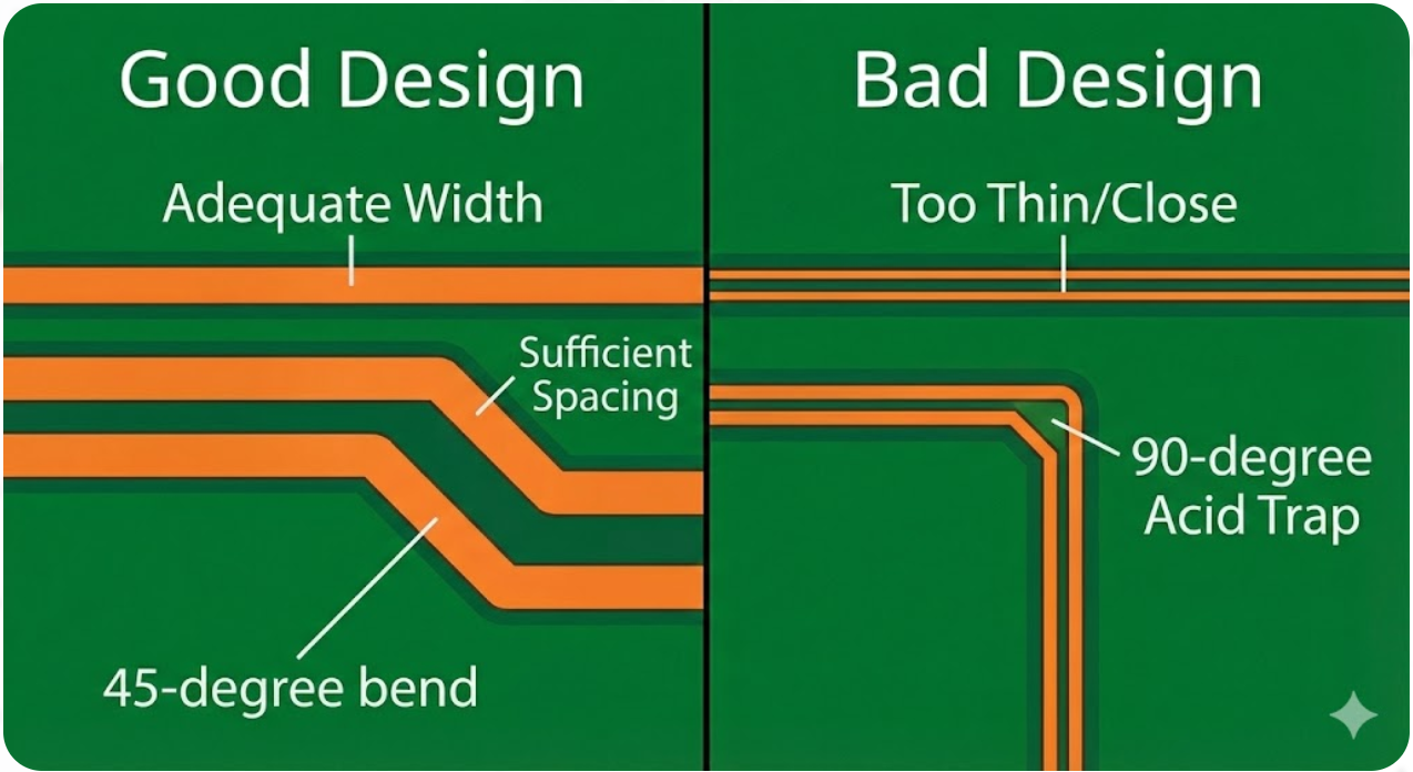
Trace geometry is at the heart of PCB manufacturability. It is at the interface of the capability of ECAD tools to draw and the reliability of fabrication processes. In modern design, software can produce very thin traces with very small clearances. But when it comes to real-world manufacturing processes, these finer details are physically impossible to achieve. It happens due to the weight of copper and the variability of etching processes. Best practice PCB DFM guidelines are thus aimed at establishing safe and repeatable geometries.
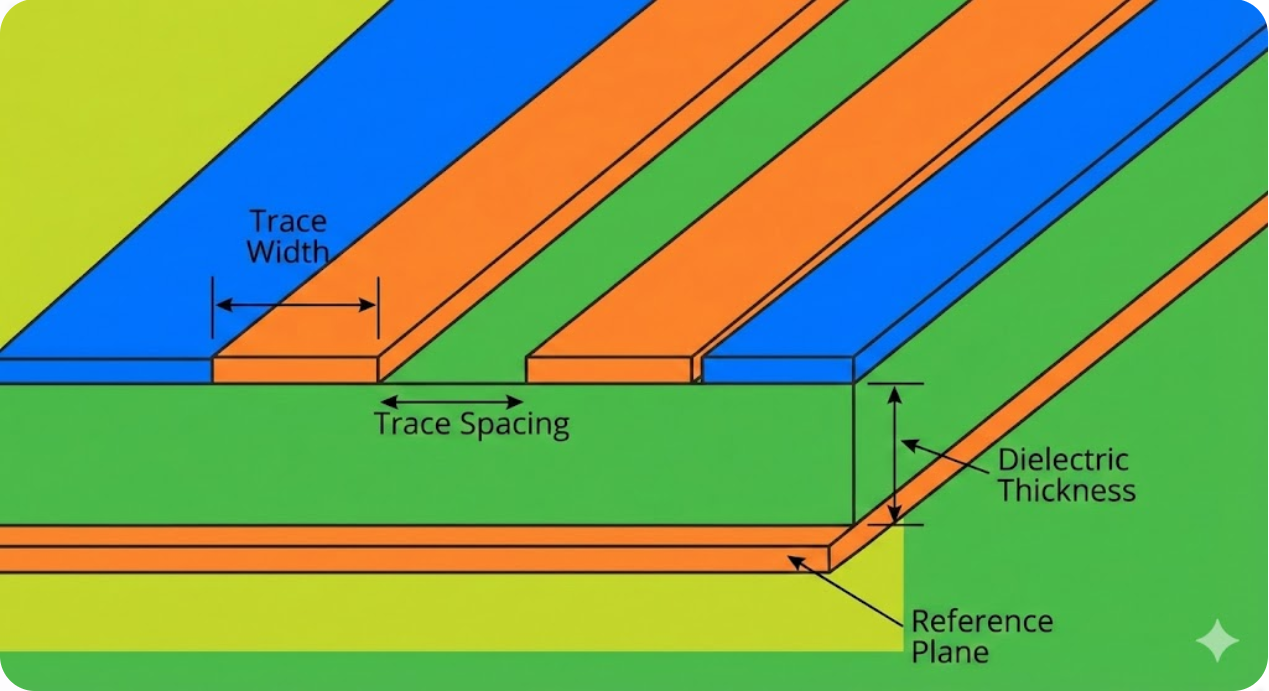
DFM considerations are used to ensure adequate trace width depending on the copper thickness. The tool finds out etching tolerance, shorts and over-etching regions. A trace width or an annular ring that is only slightly acceptable on a CAD board would be intolerable when fabrication variations are added. Overall, a designer should add a margin in the design instead of pushing towards theoretical limits.
Via Placement, Hole Size, and Panelization Rules
Vias are essential, but they are also frequently causing errors in DFM. Some common via-related DFM issues are:
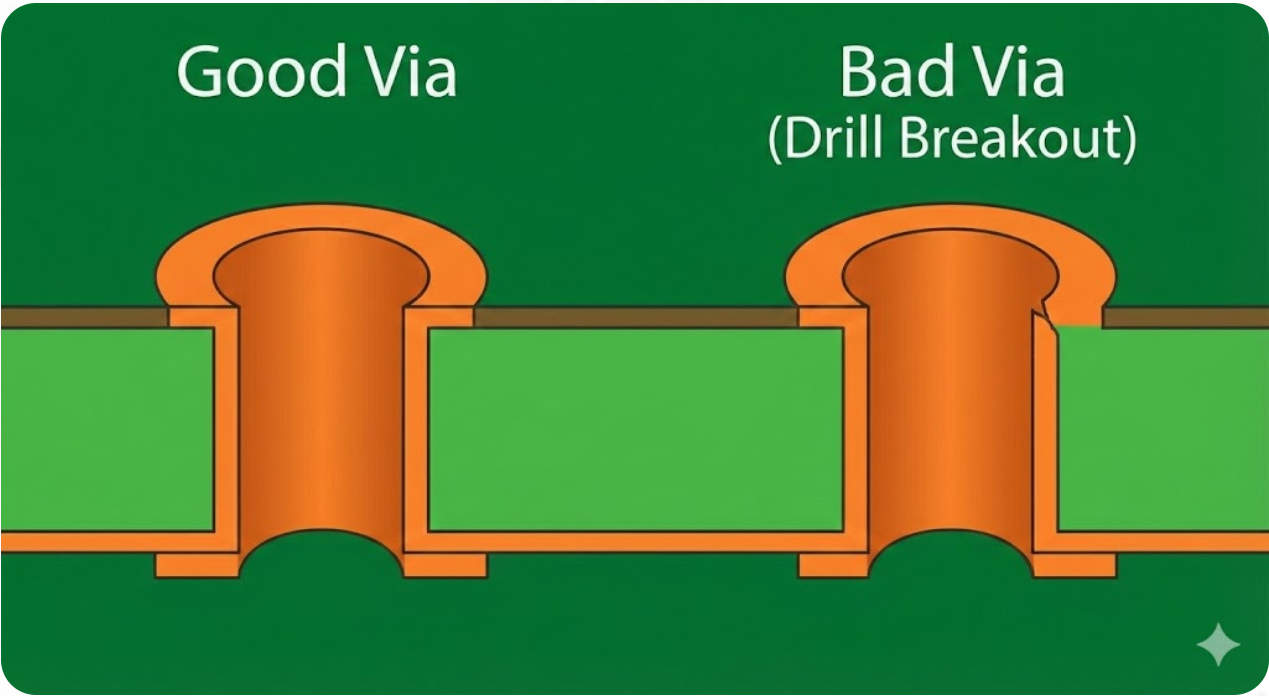
- Drill sizes too close to fabrication limits
- Insufficient pad size around vias
- Vias are placed too close to the board edges
- Vias inside component pads without proper planning
Hole size selection in PCB design may go beyond nominal values. Designers must take into account the drill tolerance, which may change the position or diameter of holes slightly, plating thickness, which decreases the finished hole size at the end of copper deposition, and aspect ratio constraints, which apply to the reliability of hole plating in thick boards. Ignorance of these aspects may result in improperly plated vias, unreliable interconnection or even failure to fabricate.
Panelization is another overlooked area. Boards must fit efficiently into manufacturing panels while respecting tooling holes, fiducials, and breakaway tabs. Ignoring panelization early can result in costly redesigns or manual assembly steps.
Soldermask, Silkscreen, and Surface Finish Considerations
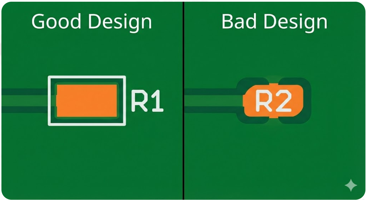
Soldermask errors are among the most common causes of assembly defects:
- Maintaining minimum soldermask dam widths
- Avoiding soldermask slivers between pads
- Preventing mask overlap on exposed copper pads
Silkscreen can still cause manufacturing issues if:
- Text overlaps pads
- Reference designators are unreadable
- Ink bleeds into solderable areas
Surface finish selection also impacts DFM:
- HASL may affect fine-pitch components
- ENIG improves flatness but increases cost
- OSP requires careful handling
Performing Effective PCB DFM Analysis
Leveraging Free DFM Tools and Software Integrations
One of the biggest misconceptions is that DFM requires expensive software. In reality, many manufacturers now offer PCB-free DFM tools. In this way, now even individual designers can analyse their layouts automatically. These tools typically:
- Check against fabrication limits
- Identify spacing and mask violations
- Highlight assembly risks
Many ECAD tools also integrate DFM checks directly into the design environment, allowing engineers to fix issues before exporting files.
Step-by-Step Review Process for Common Issues
A good PCB DFM analysis is based on a systematic progression that is similar to the real manufacturing process. Placing the correct sequence of steps first is a sure way of solving the underlying fabrication problems before proceeding to assembly and mechanical concerns. It helps to minimise re-work, which is expensive at later stages of the process.
1. Fabrication checks focus on whether the board can be reliably manufactured:
- Trace width and spacing to account for copper weight and etching tolerances
- Drill sizes and aspect ratios to ensure proper plating and mechanical strength
- Copper balance and plane continuity to avoid warpage and uneven etching
2. Assembly checks verify that components can be placed and soldered without defects:
- Component spacing for automated pick-and-place accuracy
- Soldermask openings to prevent solder bridging or insufficient wetting
- Fiducial placement for reliable alignment during assembly and inspection
3. Panel and mechanical checks ensure compatibility with production tooling:
- Board outline accuracy to avoid routing or depanelization issues
- Edge clearances for connectors, components, and tooling
- Panelization compatibility with standard manufacturing fixtures and processes
The iterative nature of PCB DFM analysis at every significant design milestone, instead of conducting it as a final analysis, significantly minimises manufacturing risk, final-stage modifications and serves to minimise overall development risk.
Interpreting Feedback and Prioritising Fixes
Not all DFM warnings are equally important. Some point to critical issues that can lead to fabrication or assembly failures, while others are just suggestions for optimisation. Treating all warnings with the same sense of urgency can result in design changes.
A better way is to immediately address violations that impact basic manufacturability by carefully considering assembly-related warnings that can impact yield or solder quality. It is risky to blindly ignore DFM feedback, but it is inefficient to blindly fix everything. The real value of DFM is the application of engineering judgment to determine what issues are really important for reliable and cost-effective production.
Transforming Designs with DFM-Driven Improvements
Reducing Fabrication Errors and Assembly Complications
DFM-based designs are also very beneficial in enhancing the manufacturing results by matching the design intention with practical fabrication and assembly resources. Boards that are always subjected to DFM guidelines have higher fabrication yield, fewer assembly defects and less rework. Most of the typical production surprises include, but are not limited to, broken annular rings, tombstoned passive components, solder bridges and open joints; they are not design errors in the electrical sense, but manufacturability oversights that DFM is explicitly designed to avoid. By solving these problems at the outset, the engineers develop designs that flow through fabrication and assembly without problems, and the optimal outcome would be a quiet production floor with no calls to the factory in an emergency.
Achieving Cost Savings and Faster Production Cycles
They are not only costly in regard to scrap boards, but also waste time, poor schedules, and the repetition of prototypes. Effective PCB design of manufacturing processes is used to minimise the amount of manual assembly or touch-ups required, and the use of panels during the manufacturing process. The result of these is direct improvements in the lead time and more predictable production schedules. DFM optimisations in small increments will save high costs when applied to hundreds or thousands of boards. Practically, the PCB that is cheapest may not necessarily be the one of the cheapest materials, but the one that was designed properly and produced successfully the first time.
Enhancing Overall Board Performance and Durability
DFM also helps in enhancing electrical and mechanical performance in addition to manufacturability and cost. DFM-based designs will have more stable copper geometries, stronger and more robust solder joints, and fewer mechanical stress concentrations. These enhancements enhance thermal cycling resistance, vibration, and stress in long-term operation. Consequently, boards that have been designed using DFM in mind tend to be more reliable and have a longer service life than those that only pass the schematic checks and electrical rule checks without respect to how the board is actually going to be constructed.
Best Strategies for Incorporating DFM Early
Collaboration Tips with Manufacturers During Design
Indeed, manufacturers are not to be considered as an external constraint, but they are an extension of the design team. The initial cooperation enables designers to know what can be fabricated, set tolerances, and desired design principles prior to making a layout decision. Early review of manufacturing capabilities, sharing of early stackups, and solicitation of desirable rule sets can be used to remove assumptions that frequently result in redesigns in later design phases. This initial communication averts the expensive last-minute alterations and creates a working relationship in which both designers and manufacturers are labouring on a single task of producing a product that is reliable and that can be manufactured.
Building DFM Checklists into Your Workflow

One of the most successful tools that can be used to avoid manufacturing problems is a properly designed DFM checklist. The designers can detect issues by checking trace and spacing limits, drill and via constraints, soldermask and silkscreen rules, as well as assembly and panelization needs, prior to the release of files. Incorporating DFM checks into the regular design process would turn manufacturability into a design habit. Such a strategy, in the long run, enhances the results of production besides giving a designer an intuition of what will and will not work on the factory floor.

Frequently Asked Questions (FAQ)
What are PCB DFM guidelines?
They are rules and best practices that ensure PCB designs can be manufactured and assembled reliably.
What is PCB DFM analysis?
An automated or manual process that checks a PCB design against manufacturing constraints.
Are the free PCB DFM tools reliable?
Yes. While not exhaustive, they catch the majority of fabrication and assembly issues.
Is DFM necessary for hobby projects?
Absolutely. Even small batches benefit from fewer errors and lower costs.
Popular Articles
Keep Learning
Creating Clear and Professional Reference Designators for Better PCB Assembly
Key Takeaways Reference designators are essential for accurate PCB assembly, debugging, and maintenance. Use minimum 0.8 mm text height and 0.15 mm line width for clear silkscreen printing. Keep designators on solder mask with proper clearance from pads and vias. Maintain consistent font, size, and orientation across the board. For high-density designs, use an assembly drawing instead of crowded silkscreen. Always run DFM checks to avoid overlapping or missing labels. Ever wonder about the little labe......
How to Design a PCB with Flux.ai (Step-by-Step Guide)
Key Takeaways This step-by-step Flux PCB design tutorial demonstrates the complete workflow by creating a compact 15 × 15 mm USB 2.0 hub, refining the layout, routing high-speed differential traces, and preparing manufacturing files for JLCPCB PCB fabrication and assembly. We are all hearing news; new AI models are being released every month. And it has finally reached the schematic editor. Flux.ai is a browser-based AI PCB design tool with a built-in AI agent that behaves like a junior hardware engin......
How to Design Your Own Keyboard PCB: From Layout to Firmware
Designing a custom keyboard PCB is one of the most rewarding entry points into practical electronics. You not only get a really useful product on your desk, but also you learn schematic capture, matrix scanning, footprint selection, USB, and firmware. Most of the hardware engineers use the same skills that show up on professional boards. This guide walks the entire build from choosing switches, wiring the diode matrix, adding the microcontroller and USB-C, laying out the board, and flashing QMK or VIA......
Don't Let Design Errors Ruin Your Hardware: The Complete Guide to PCB Design Verification
Key Takeaways PCB design verification is the systematic process of validating layouts against electrical, signal integrity, and manufacturing rules before production, preventing costly board respins and launch delays. Schematic verification through Electrical Rules Check (ERC) catches floating inputs, power shorts, and footprint mismatches before layout begins. Design Rule Checking (DRC) ensures trace widths, clearances, and via sizes comply with your fabricator's manufacturing tolerances, especially ......
How to Determine the Right PCB Voltage Clearance for Safe and Reliable Designs
Key Takeaways Clearance is the air gap; Creepage is the surface path — both essential for high-voltage safety. Base spacing on peak voltage and follow IPC-2221 / IEC 60664-1 standards. Major factors: voltage, pollution degree, CTI, altitude, and conductor location. Use isolation slots, guard rings, and conformal coating to optimize spacing. Always run clearance calculations, DFM checks, and Hipot testing before production. Why do two copper traces that work fine at 5V suddenly arc over and burn at 400......
Mastering PCB Footprints: Design Best Practices for Reliable Manufacturing
Key Takeaways A PCB footprint (land pattern) translates component datasheet dimensions into copper pads, solder mask openings, paste apertures, silkscreen, and clearance areas that enable reliable soldering and assembly. Follow IPC-7351 standards and manufacturer DFM rules for pad dimensions, spacing, and layer design to minimize defects like solder bridging, tombstoning, and cracked joints. Choose between through-hole (THT) and surface mount (SMT) footprints based on electrical needs, thermal perform......