AI PCB Design: From Prompt to PCB with EasyEDA Pro
12 min
- What Is AI PCB Design and How It Works
- AI PCB Design Workflow: How the Pieces Fit Together
- How to Set Up the AI PCB Design Workflow
- Getting Better Results from AI PCB Design: Prompting for Hardware
- Advanced AI PCB Design Patterns
- Troubleshooting Quick Reference for AI Design
- FAQ about AI PCB Design
- Conclusion: Why AI PCB Design Matters
Key Takeaways
- AI PCB design uses AI agents to automate schematic creation, component selection, layout, and verification inside a real EDA editor — not just generate images.
- The workflow connects EasyEDA Pro to an AI coding agent (Claude Code or Codex) through the EasyEDA API Gateway, the open-source API Skill, and a local bridge server.
- Setup takes about ten minutes and is fully local-first: designs, API calls, and intermediate code never leave your machine.
- Because the agent places real library parts, the exported BOM maps to real part numbers that JLCPCB can source and assemble.
Hardware design has always had a bottleneck that has nothing to do with physics: the hours spent dragging symbols, renaming nets, and nudging traces into place. What if that mechanical work could be delegated to an AI agent — one that doesn't just draw a picture of a circuit, but operates the actual EDA editor, placing real symbols, real wires, and real footprints you can send straight to fabrication?
AI PCB design uses AI agents to automate parts of schematic creation, component selection, PCB layout, and design verification within an EDA environment. That workflow is no longer hypothetical. With the EasyEDA API Gateway and the open-source EasyEDA API Skill, you can connect EasyEDA Pro to an AI coding agent such as Claude Code or OpenAI Codex, and drive your design with plain language:
Example Prompt
"Design an ESP32-S3 sensor expansion board with an I²C temperature sensor, USB-C power, and a 2-layer layout — circuit design and PCB included."
One sentence in; a real, editable EasyEDA project out. This article walks through how the system works, how to set it up, and how to get the most out of it.
What Is AI PCB Design and How It Works
AI PCB design uses AI agents to automate structured tasks within an electronic design automation (EDA) environment. AI coding agents have become remarkably good at following structured tool interfaces. Give an agent a well-documented API and a goal, and it will plan multi-step operations, check its own work, and recover from errors.
EDA software is, at its core, a structured environment: every component has a UUID, every pin has coordinates, every net has a name. That makes it an almost ideal target for agent-driven automation.
EasyEDA Pro already exposes a rich JavaScript API for extensions. The API Gateway turns that API into a remote-callable interface, and the API Skill packages the documentation, conventions, and helper scripts that an AI agent needs to use it correctly.
With this setup, an AI agent can translate a natural-language design request into operations inside the actual EDA editor. The result is not "AI draws a schematic image" — it is AI operating the editor itself, producing native design files you own and can refine.
AI PCB Design Workflow: How the Pieces Fit Together
The pipeline has three components, all running locally on your machine:
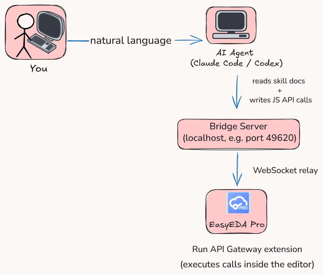
- The AI agent is the planner. It reads your request, consults the skill's API reference, and emits JavaScript that calls EasyEDA's extension API — create a component here, createNetFlag there, autoRouting, run ERC, and so on.
- The EasyEDA API Skill is the agent's instruction manual. It ships with structured documentation of the API surface (schematic primitives, PCB primitives, libraries, documents, editor control) plus the bridge tooling. Without this context, the agent would have to guess at method names; with it, the agent can call the API fluently.
- The Bridge Server is a lightweight local HTTP/WebSocket relay. The agent POSTs JavaScript snippets to it; the bridge forwards them to whichever EasyEDA window is connected and returns the results.
- The Run API Gateway extension lives inside EasyEDA Pro. It listens for the bridge, executes the incoming JavaScript in the editor's extension runtime, and streams results back.

Two properties of this design are worth highlighting:
- Local-first. Nothing leaves your machine. Your designs, your API calls, and the AI's intermediate code all stay on localhost.
- Inspectability. Every operation is explicit JavaScript. You can read exactly what the agent did, replay it, or lift it into your own automation scripts.
How to Set Up the AI PCB Design Workflow
What You'll Need
Total setup time is about ten minutes.
| Tool | Role | Where to get it |
|---|---|---|
| EasyEDA Pro (Professional Edition) | The design editor that executes everything | easyeda.com/page/download |
| Run API Gateway extension | Receives and executes external API calls inside EasyEDA | https://ext.lceda.cn/item/oshwhub/run-api-gateway |
| EasyEDA API Skill | API documentation + bridge server for the AI agent | github.com/easyeda/easyeda-api-skill |
| Claude Code or Codex | The AI agent that writes the API calls | Your existing agent CLI |
1Enable the Gateway in EasyEDA Pro
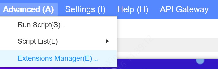
- Launch EasyEDA Pro and open Advanced → Extensions Manager.
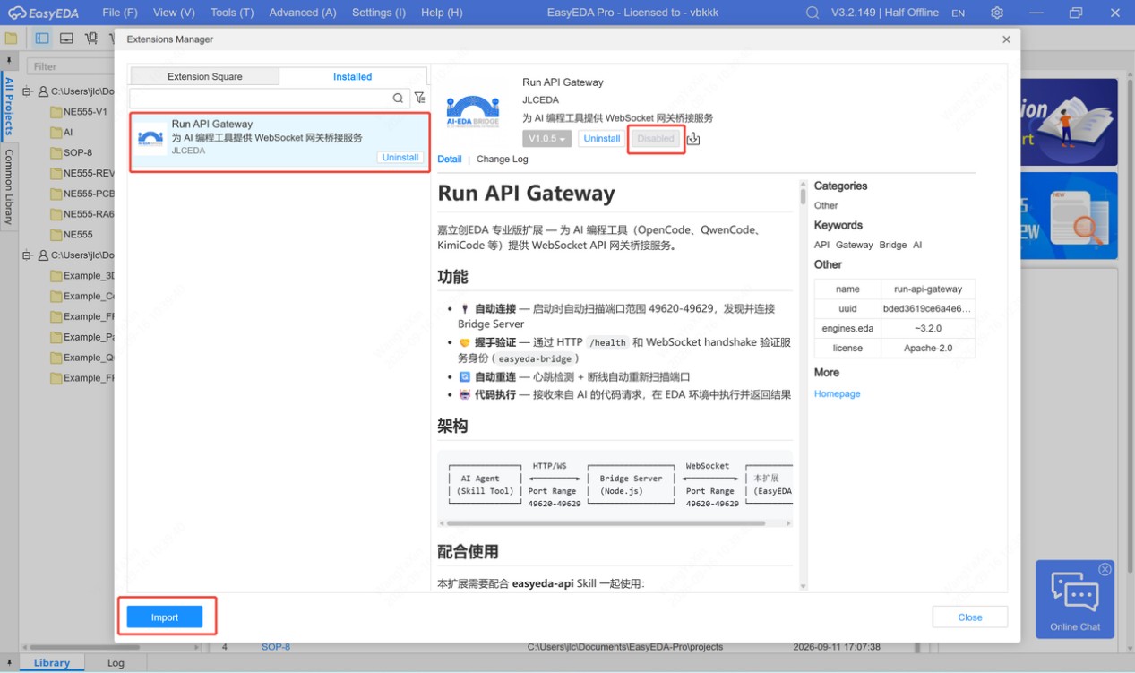
- Download
run-api-gateway_v1.0.5.eextfrom jlc-ext.com and import it into the Extensions Manager. - Switch to the Installed tab, select Run API Gateway, and click Disabled so it toggles to Enabled.
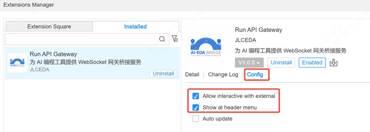
Open the extension's Config and turn on both options:
- Allow interact with external — permits communication with programs outside EasyEDA.
- Show at header menu — adds the API Gateway entry to the top menu bar for quick access.
EasyEDA Pro is now listening for a bridge connection.
2Start the Bridge Server
In a terminal:
git clone https://github.com/easyeda/easyeda-api-skill
cd easyeda-api-skill
npm install
npm run build:docs   # builds the API reference the AI will read
npm run server       # starts the local bridge (default port 49620)
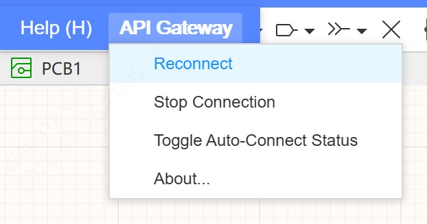
Leave this terminal running. Then, back in EasyEDA Pro, open the API Gateway menu and click Reconnect.
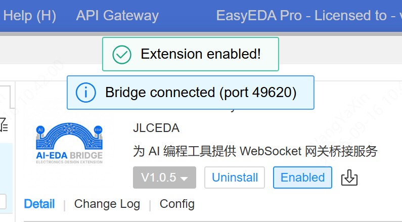
A successful handshake shows:
Bridge connected (port 49620)
If you ever restart the bridge server, reconnect from this menu — the WebSocket session does not survive a server restart.
3Install the Skill for Your Agent
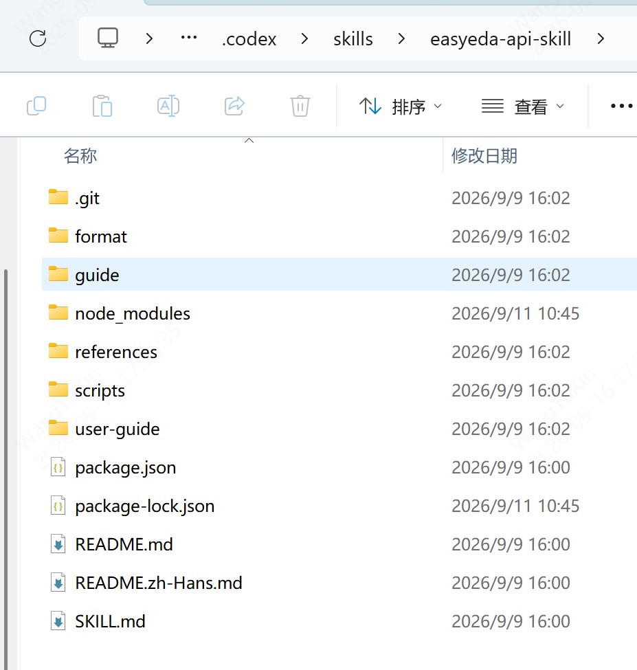
Copy the skill package into your agent's skills directory so it loads on startup:
- Claude Code:
~/.claude/skills/easyeda-api-skill/ - Codex:
~/.codex/skills/easyeda-api-skill/
On Windows, ~ maps to your user profile (e.g. C:\Users\jlc\.codex\skills\easyeda-api-skill). Restart the agent and it will discover the skill automatically.
4Design with a Sentence
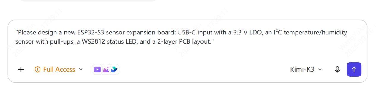
With the bridge connected and the skill loaded, invoke the skill and describe your board:
"Please design a new ESP32-S3 sensor expansion board: USB-C input with a 3.3 V LDO, an I²C temperature/humidity sensor with pull-ups, a WS2812 status LED, and a 2-layer PCB layout."
Watch what the agent does — this is where it gets interesting:
Planning
The agent decomposes your sentence into subsystems: power input, regulation, MCU, sensor, LED, decoupling.
Library lookups
It searches the component library for each part, resolving real footprints and symbol UUIDs rather than hallucinating them.
Placement
It creates each symbol at deliberate coordinates, keeping the schematic readable — power on one side, signal chain flowing left to right.
Connectivity
It adds net labels and power flags (VCC, GND, 3V3, SDA, SCL...) so the design is electrically meaningful, then wires up what needs wires.
Verification
It can run ERC-style checks, enumerate nets, and fix what it finds — the same loop a careful engineer runs, compressed into seconds.
Layout
Switching to the PCB domain, it places footprints, respects the board outline, and routes.
Every step lands in your open EasyEDA project as native, editable objects. Nothing is locked in.
Getting Better Results from AI PCB Design: Prompting for Hardware
A few habits dramatically improve what the agent produces:
- Name the nets and pins you care about. "I²C on SDA=GPIO8, SCL=GPIO9, with 4.7 kΩ pull-ups" gives the agent exact constraints instead of letting it choose.
- State the power architecture explicitly. "USB-C 5 V in → LDO → 3V3 rail; everything on 3V3 except the LED's 5 V" prevents the classic mistake of mixed rails.
- Reference real parts when it matters. If you already know the part number or the exact module (e.g. a specific dev board as the MCU), say so — the agent will place that symbol instead of a generic one.
- Iterate in conversation. The bridge session is stateful. "Move the sensor block to the top-right" or "rename that net to VBUS" are perfectly valid follow-ups. Treat the agent like a junior engineer sitting at your second monitor.
- Ask for checks. "Run ERC and list any unconnected pins" turns the agent from a draftsman into a reviewer.
Advanced AI PCB Design Patterns
Once the basics work, the same pipeline scales to serious work:
- Repeatable design blocks. Capture a proven subsystem (e.g. your standard USB-C + LDO front end) as a snippet of API calls, and have the agent instantiate it across projects — poor-man's hierarchical reuse, fully scripted.
- Design generation from data. Feed the agent a table of connectors, sensors, or pin mappings from a spreadsheet and let it synthesize the schematic page-by-page.
- BOM discipline. Because the agent places real library parts, the exported BOM maps to real part numbers — the same parts JLCPCB can source and assemble, closing the loop from prompt to production.
- Batch edits. "Rename every net matching SPI_* to QSPI_*" or "swap all 0603 capacitors to 0402" are one-prompt operations instead of an afternoon of clicking.
Troubleshooting Quick Reference for AI Design
| Symptom | Likely cause | Fix |
|---|---|---|
| Agent calls fail with connection errors | Bridge restarted, WebSocket dropped | API Gateway → Reconnect in EasyEDA |
| Nothing appears on the canvas | Wrong document/page active | Open the target schematic in EasyEDA first; ask the agent to enumerate and activate it |
| Net labels placed but no wires after auto-route | Labels not exactly on pin endpoints | Nudge labels onto pin connection points, or ask the agent to align them |
| Project creation API returns empty | Some APIs target cloud/team projects | Create the project manually, then let the agent work inside it |
| Port already in use | Stale bridge process | Stop the old node process, restart npm run server |
FAQ about AI PCB Design
Q: What is AI PCB design?
AI PCB design uses AI agents to automate structured tasks within an electronic design automation (EDA) environment. Instead of only generating images or suggestions, an AI agent can interact with the actual EDA editor through APIs to create and modify schematic and PCB design elements. In this workflow, the resulting files remain native, editable, and available for further review and refinement by the designer.
Q: Can AI agents actually design a PCB in EasyEDA Pro?
Yes. With the EasyEDA API Skill and API Gateway, AI coding agents can interact with EasyEDA Pro through its Extension API. The agent can perform operations such as creating components, managing nets, working with PCB objects, running routing operations, and checking the design. EasyEDA's Extension API provides JavaScript interfaces for developing custom functions within the editor.
Q: What is the EasyEDA API Skill used for in AI PCB design?
The EasyEDA API Skill provides AI agents with structured API documentation, instructions, examples, and bridge tooling for working with EasyEDA Pro. It helps the agent identify and call the appropriate API functions instead of guessing method names. The current open-source skill also supports a WebSocket Bridge for connecting AI tools with a running EasyEDA Pro client.
Q: Can AI PCB design replace a PCB designer?
AI PCB design is better understood as an automation and assistance workflow rather than a replacement for engineering review. AI agents can handle repetitive operations and execute structured design tasks, but the designer still needs to inspect the schematic and PCB, review the results, make engineering decisions, and refine the design before manufacturing. This human-in-the-loop approach is also consistent with the industry's current movement toward tool-integrated and continuously validated AI workflows.
Q: Can an AI-designed PCB be manufactured with JLCPCB?
Yes. When the AI agent creates a native EasyEDA Pro project using real components, footprints, nets, and other design data, the project can continue through the normal PCB manufacturing workflow after review and refinement. The exported BOM can map to real part numbers that JLCPCB can source and assemble, providing a path from AI PCB design to PCB fabrication and assembly.
Conclusion: Why AI PCB Design Matters
The interesting shift here isn't that AI can draw — it's that AI can now operate professional tools through their real interfaces. The schematic the agent produces is the same schematic you'd draw by hand: same parts, same nets, same ERC, and a direct path from AI PCB design to JLCPCB fabrication and assembly. The difference is that the hours of mechanical work collapse into minutes of conversation, and every design decision remains yours to inspect, override, and refine.
Because the agent works with real library parts, the exported BOM can also map to real part numbers that JLCPCB can source and assemble. This helps connect the AI PCB design workflow with the next stage of the process: turning an editable design into a physical PCB.
The toolchain is open, local, and free to try. Clone the skill, connect the gateway, and describe the board you've been meaning to build.
Popular Articles
• AI Tools for PCB Design: Which Tool Fits Your Workflow Stage?
• GPT-6 Astra PCB Design in KiCad: From Brief to Verified Native Project
• GPT-6 Astra PCB Design in EasyEDA Pro: What Worked, What Failed, and What We Learned
• AI PCB Design: From Prompt to PCB with EasyEDA Pro
• How to Design Your Own Keyboard PCB: From Layout to Firmware
Keep Learning
GPT-6 Astra PCB Design in KiCad: From Brief to Verified Native Project
Key Takeaways What OpenAI published: The launch page features a 15-second condensed clip of GPT-6 Astra performing PCB layout in KiCad. What the model did: It turned a four-line brief into a 44 × 34 mm, two-layer PCB, covering the circuit, footprints, component placement, routing, and a native two-sheet schematic. Where the work went: Placement and routing were only part of the work. Two linked schematic sheets, project-local libraries, and UUID-based links between 45 components and their footprints w......
GPT-6 Astra PCB Design in EasyEDA Pro: What Worked, What Failed, and What We Learned
Key Takeaways What was tested: GPT-6 Astra was given access to a native EasyEDA Pro 3.2.149 installation and asked to design a stereo TPA3116D2 amplifier from a four-line written brief. What it produced: The run resulted in a 44 × 34 mm, two-layer PCB with 40 SMD components and an editable native EasyEDA Pro project with embedded libraries. Where it failed: The first complete import opened cleanly and looked plausible, yet the initial native verification reported 50 association mismatches involving 12......
AI Tools for PCB Design: Which Tool Fits Your Workflow Stage?
AI tools can now assist with PCB architecture, schematic generation, component selection, placement, routing, and design verification. However, different tools target different stages of the PCB workflow. This guide compares AI tools for PCB design based on what they actually do, what inputs they require, and where they fit within a real engineering workflow. In this guide, you will learn: The 6 types of AI PCB tools and the input each one needs What AI PCB design tools do, compared stage by stage How......
EasyEDA Pro vs KiCad: GPT-6 Astra PCB Design Compared
Key Takeaways What is being compared: Two versions of the same TPA3116D2 stereo amplifier project, each created by GPT-6 Astra in a different EDA tool. The comparison focuses on what you can actually do with the delivered project afterward. Ground copper: In the EasyEDA Pro project, the ground copper is stored as 28 fixed filled regions. In KiCad, it remains as two native copper zones that can automatically refill after layout changes. Verification: KiCad initially reported 46 schematic-parity issues.......
A Practical Guide to ODB Files for PCB Manufacturing
Key Takeaways All-in-One Data: ODB++ combines artwork, netlist, stackup, and drill spans in a single package. Fewer Errors: Embedded netlists allow CAM software to catch errors before production. Pre-Export Checks: Clear DRCs, close the board outline, and verify drill spans in a viewer. Best Practice: Use Gerber for quick quotes and keep ODB++ ready for engineering queries. A Gerber layer might simply say, “draw a 0.5 mm (20 mil) circle here.” ODB++ can describe that same feature as a pad on the VCC n......
AI PCB Design: From Prompt to PCB with EasyEDA Pro
Key Takeaways AI PCB design uses AI agents to automate schematic creation, component selection, layout, and verification inside a real EDA editor — not just generate images. The workflow connects EasyEDA Pro to an AI coding agent (Claude Code or Codex) through the EasyEDA API Gateway, the open-source API Skill, and a local bridge server. Setup takes about ten minutes and is fully local-first: designs, API calls, and intermediate code never leave your machine. Because the agent places real library part......