IGBT Symbol Guide: Diagram, Pins, Types & How to Read It
14 min
- IGBT Symbol Quick Reference
- What Does an IGBT Symbol Mean?
- IGBT Symbol Anatomy: What Each Element Means
- N-Channel vs P-Channel IGBT Symbols
- IGBT Symbol With a Freewheeling Diode
- IGBT vs MOSFET vs BJT
- IEC and ANSI IGBT Symbol Conventions
- How to Read an IGBT Symbol in a Schematic Step by Step
- Common Mistakes When Reading IGBT Symbols
- Conclusion
- FAQs about IGBT symbols
Key Takeaways
- Identify the terminals first: Gate (G), collector (C), and emitter (E) are the three main IGBT terminals.
- Know the symbol variants: N-channel and P-channel IGBT symbols can be compared to understand their different conventions.
- Do not rely on one drawing style: IEC and ANSI/IEEE symbols can look different even when they represent the same device.
- Check the diode separately: The anti-parallel freewheeling diode may be included in the symbol or shown as a separate component, depending on the drawing convention and application.
- Verify before connecting the gate driver: Always confirm the pinout from the manufacturer's datasheet rather than assuming the symbol matches the physical package.
An IGBT symbol can look very similar to a power MOSFET symbol, making the two easy to confuse at first glance.
In a motor power converter, misidentifying an IGBT as a MOSFET can lead to incorrect gate-drive or device-terminal connections.
Symbol variations across IEC and ANSI conventions, datasheets, and EDA libraries can also make identification less straightforward.
In this guide, you will learn:
- IGBT symbol variants, N-channel and P-channel, drawn side by side
- How to identify the gate, collector, and emitter on an IGBT symbol
- Why the emitter arrow points opposite to the MOSFET arrow
- When an anti-parallel freewheeling diode is shown with the IGBT
- How IEC and ANSI conventions represent IGBT symbols
IGBT Symbol Quick Reference
These six common variants cover the IGBT symbol forms you are most likely to encounter.
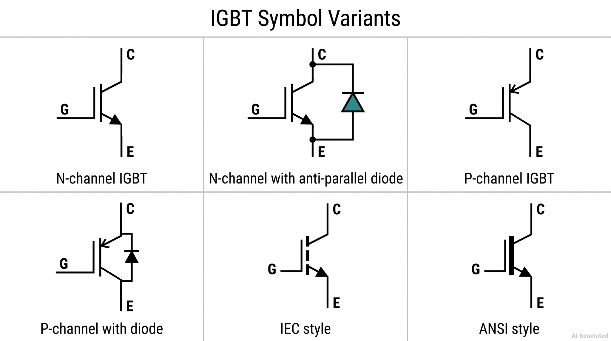
Figure: Common IGBT symbol representations
| Symbol Variant | What the Symbol Shows | Use It When | Do Not Read It As |
|---|---|---|---|
| N-channel IGBT | G, C, E, with the emitter arrow pointing away from the body | You mean the ordinary power switch | Evidence of a body diode. A standard IGBT has none |
| Three-segment body | The same terminals, channel drawn in three strokes | Your library draws the channel in segments | A different device. It is the same part |
| Circled outline | The IGBT symbol is enclosed by a circle or circular outline | Marking a packaged discrete rather than an on-die device | An electrical difference. The circle carries none |
| IGBT with anti-parallel diode | A diode is connected across C and E, with its cathode at the collector | The load is inductive, and the freewheel current needs a path | Proof that the diode is inside the part. It is often external |
| Reverse-conducting IGBT (RC-IGBT) | The same diode inside a dashed die boundary | The diode is monolithic on the same silicon | A plain IGBT beside a separate diode die |
| P-channel IGBT | The emitter arrow points toward the body | The schematic calls for the complementary device | An N-channel part. That arrow changes the device. |
The emitter arrow helps identify the IGBT type, while an anti-parallel diode indicates whether a reverse-current path is provided. For a broader overview of electronic schematic symbols, see our guide to circuit symbols.

- Turn your verified power-stage design into a professionally manufactured PCB with JLCPCB.
- Upload your Gerber files to get an instant quote for PCB fabrication and assembly.
What Does an IGBT Symbol Mean?
An IGBT symbol is a three-terminal schematic symbol representing the gate, collector, and emitter of an insulated-gate bipolar transistor.
It resembles a MOSFET but uses collector/emitter terminals and an emitter arrow.
- Gate (G) is the control terminal: The vertical plate set apart from the body, in the position a MOSFET gate occupies. It draws no meaningful steady current, so the drive power is set by how fast you charge the gate capacitance.
- Collector (C) is the high-side current terminal: The upper terminal corresponds functionally to the drain connection of a MOSFET. On a TO-247 or TO-220 package, the metal mounting tab is electrically the collector, which is why that tab is live at rail voltage.
- Emitter (E) is the low-side power terminal and gate-drive reference: The lower terminal, carrying the arrow. Gate drive is specified as VGE (gate-to-emitter), so wherever the emitter sits, your gate drive has to sit with it.
To compare the IGBT with other three-terminal transistor devices, see our complete guide to transistor symbols.
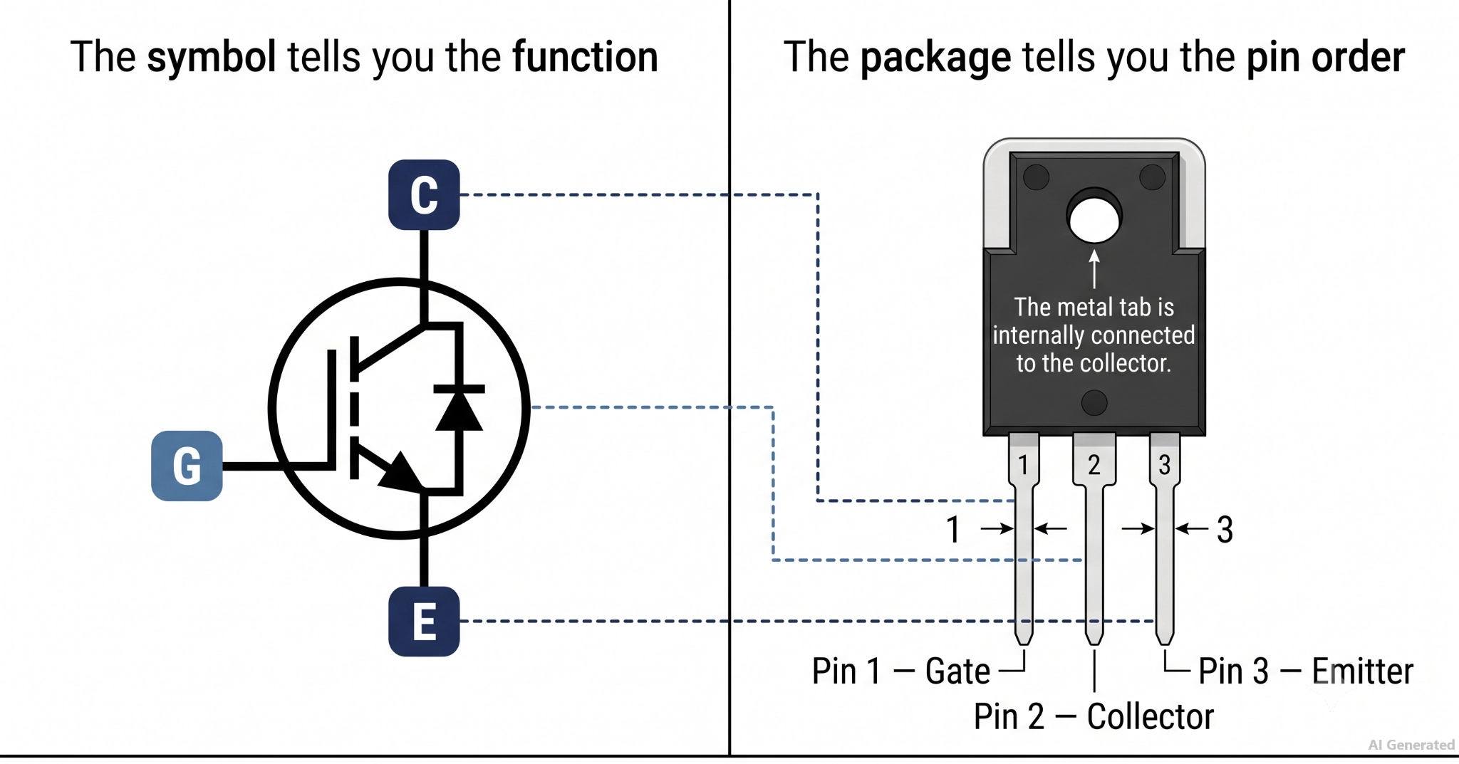
Figure: The N-channel IGBT symbol with G, C, and E labeled
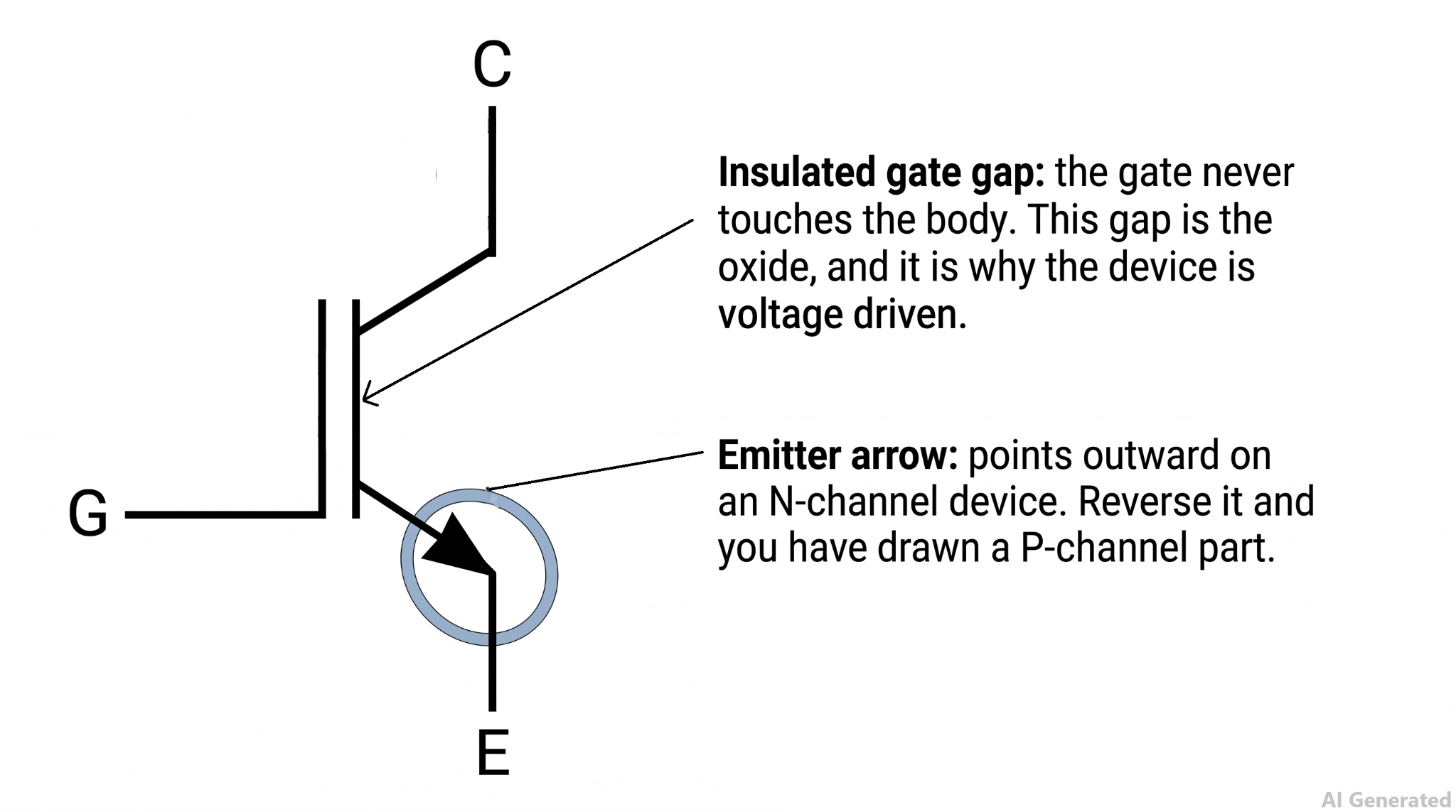
Figure: N-channel IGBT symbol
Note
The obvious question one can think of: Why does an IGBT use collector and emitter terminals instead of drain and source?
Because the output stage is bipolar. ROHM's device note puts it plainly: the PNP transistor's emitter serves as the IGBT collector, and the IGBT emitter is the N+ layer that corresponds to the source of the N-channel MOSFET.
IGBT Symbol Anatomy: What Each Element Means
An IGBT symbol uses several visual elements to identify the device and its terminals. The gate gap, device body, emitter arrow, and collector lead each provide clues for interpreting the symbol and distinguishing it from similar transistor symbols.
- The gap beside the gate: The gate is drawn as a line separated from the device body, with no direct connection between them. This gap represents the electrical insulation between the gate and the main conduction path.
- The vertical conduction bar: The body of the device, drawn either as one solid bar or as three short segments borrowed from the enhancement MOSFET outline. Both forms mean the same thing, and neither says anything about the current rating.
- The arrow on the emitter lead: A filled arrowhead pointing in the direction of conventional current at the emitter. On an N-channel device, it points away from the body.
- The plain collector lead: If both output leads carry arrows, you are looking at something that is not an IGBT.
- The gate lead position: Drawn on the left in most libraries, entering horizontally. Some house styles rotate the symbol so the gate enters from below, and the gap, the arrow, and the letters still decide what you are reading.
Note
The arrow declares device polarity, not the direction current happens to take in your circuit. During freewheeling, current flows through the diode from emitter to collector while that arrow still points the other way.
N-Channel vs P-Channel IGBT Symbols
Exactly one line differs between the two. On an N-channel IGBT symbol, the emitter arrow points away from the body; on a P-channel symbol, it points into the body. Everything else, terminal names included, is identical.
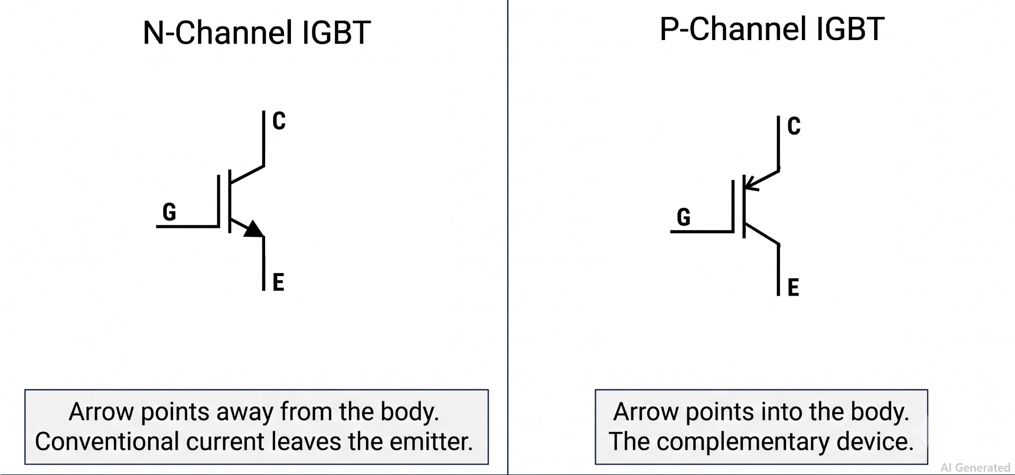
Figure: N-channel and P-channel IGBT symbols
- N-channel, arrow pointing outward: Turns on with the gate positive with respect to the emitter, typically around +15 V. Current enters the collector and leaves the emitter. This is the device inside essentially every motor drive, inverter leg, and induction hob you will open.
- P-channel, arrow pointing inward: Turns on with the gate negative with respect to the emitter. Current enters the emitter and leaves the collector.
- What does not change: The terminal letters, the gate gap, the conduction bar, and the plain collector lead are drawn identically for both polarities.
Note
P-channel IGBTs are rare in production power designs, and the EDA libraries record that. KiCad's Device library ships eight generic IGBT symbols, and every one of them is N-channel. No generic P-channel IGBT symbol ships at all. On an N-channel MOSFET symbol, the body arrow points inward, the opposite sense, as our MOSFET symbol guide sets out.
IGBT Symbol With a Freewheeling Diode
A freewheeling diode is shown anti-parallel to the IGBT, with its cathode connected to the collector and its anode connected to the emitter. The diode is not an intrinsic part of a conventional IGBT; it may be provided as a separate external component, co-packaged with the IGBT, or integrated into the same semiconductor die in a reverse-conducting IGBT (RC-IGBT).
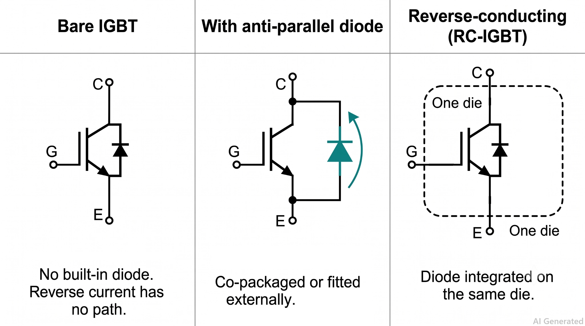
Figure: Three IGBT symbol variants: a bare IGBT, an IGBT with a co-packaged anti-parallel diode, and a reverse-conducting IGBT with an integrated diode.
- Bare IGBT, no diode: The part offers no reverse path. For example, the IRG4PF50W, a 900 V, 51 A device in TO-247AC, is drawn this way, and an inductive load switched by it needs an external diode.
- IGBT with a co-packaged diode: The diode is a separate die inside the same package. For example, the STGP7NC60HD from STMicroelectronics (600 V, TO-220) and the FGH75T65SQD from onsemi (650 V, 75 A, TO-247-3) both ship this way, and their datasheets quote a separate junction-to-case thermal resistance for the diode.
- Reverse-conducting IGBT (RC-IGBT): The diode is monolithically integrated on the same die.
Without an appropriate freewheeling path, switching an inductive load can generate excessive voltage overshoot and damage the IGBT.
The collapsing magnetic field drives the collector well past the rated VCES, and a 600 V part fails in microseconds. Cathode orientation is the detail that people reverse. The cathode bar goes to the collector, so the diode blocks while the IGBT conducts and only carries current when the load forces it the other way.
See our diode symbol guide for a detailed explanation of diode polarity.
IGBT vs MOSFET vs BJT
Look at two places and all three devices separate cleanly.
The control terminal tells you whether the device is voltage or current-controlled, and the arrow position tells you which family it belongs to.
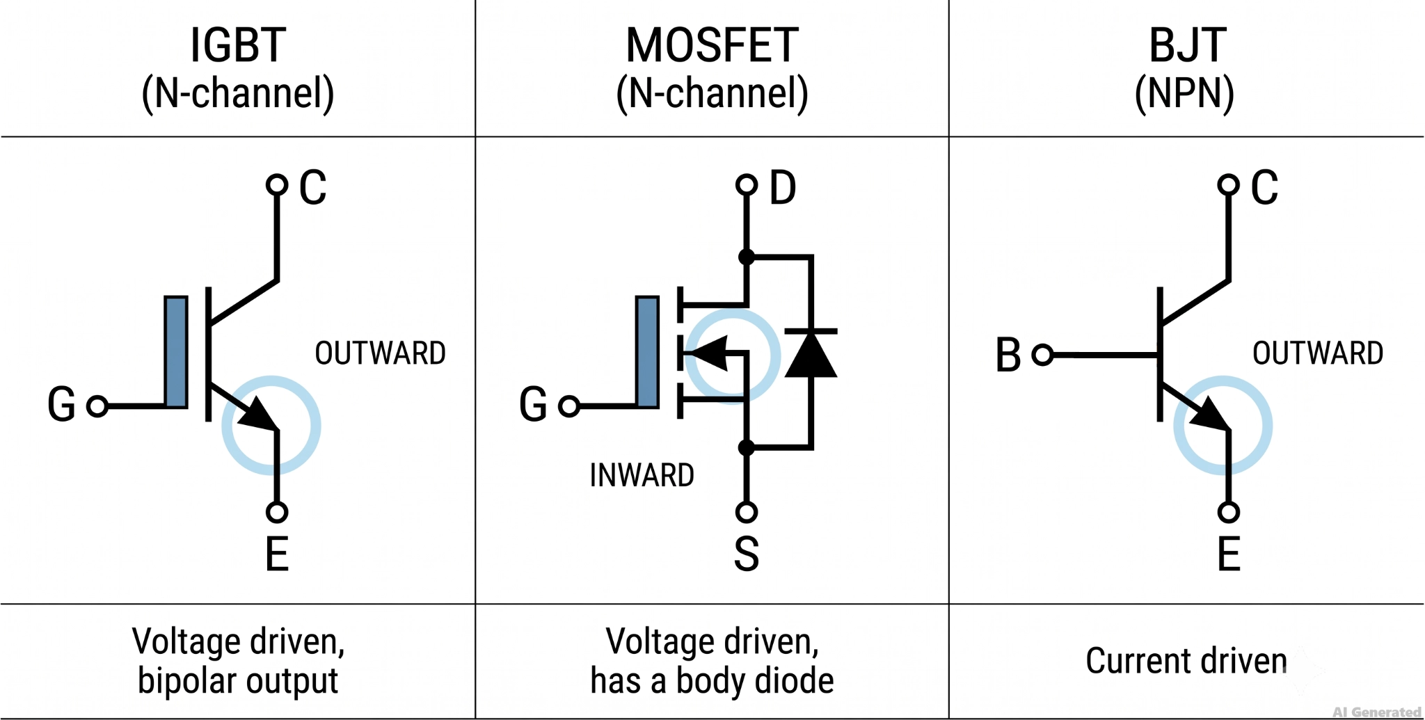
Figure: Symbols for IGBT, MOSFET, and BJT
| Detail on the Symbol | IGBT | MOSFET | BJT | What It Tells You |
|---|---|---|---|---|
| Control terminal | Gate plate, separated by a gap | Gate plate, separated by a gap | Baseline touching the body | A gap means voltage-controlled; a contact means current-controlled |
| Terminal names | Collector, Emitter | Drain, Source | Collector, Emitter | Names follow the output stage, not the input |
| Arrow location | On the emitter lead | On the body lead, mid-channel | On the emitter lead | An arrow entering mid-channel means MOSFET |
| Arrow direction, N-type | Away from the body | Into the channel | Away from the body | The N-channel IGBT and the NPN share a sense; the N-MOSFET does not |
| Intrinsic reverse diode | None | Body diode, inherent to the structure | None | Only the MOSFET hands you a free reverse path |
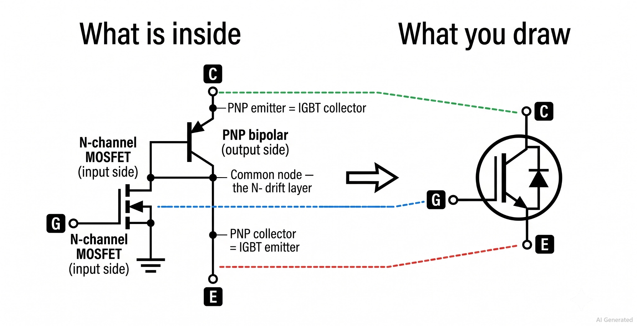
Figure: The IGBT equivalent circuit, an N-channel MOSFET driving a PNP transistor
The figure above explains why the symbol is a genuine hybrid rather than a compromise.
ROHM's structure note describes the N-channel MOSFET drain and the PNP base as one common region, the N- drift layer, with the PNP emitter serving as the IGBT collector. The input really is a MOSFET, and the output really is a bipolar transistor, so the symbol reports both halves truthfully.
IEC and ANSI IGBT Symbol Conventions
Neither IEC 60617 nor ANSI/IEEE 315 fixes one single IGBT outline. Both govern how symbols are drawn on diagrams, both accept the three-terminal insulated-gate form, and the visible differences between them are matters of style rather than meaning.
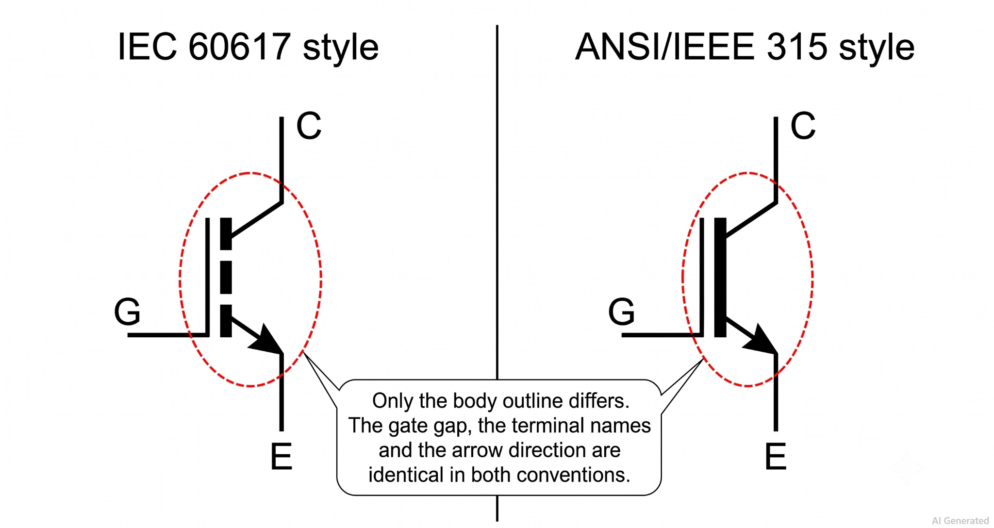
| What Differs | IEC 60617 Practice | ANSI/IEEE 315 Practice | What It Means for Your Schematic |
|---|---|---|---|
| Enclosing circle | Usually omitted | Commonly retained for a packaged discrete | No electrical change with circle and non-circle |
| Conduction bar | A single solid bar is common | The three-segment channel is common | The same device. Pick one form per sheet rather than mixing them |
| Terminal lettering | G, C, E placed outside the body | G, C, E, identically | The letters are the one part of the drawing you can always trust |
| Emitter arrow | Filled head, pointing with conventional emitter current | The identical convention | Arrow sense is where both standards agree, so it is safe to read |
It turns out that ANSI/IEEE Std 315-1975, reaffirmed in 1993, predates the commercial IGBT altogether. The standard has no dedicated IGBT entry, so vendors extended the existing transistor symbols in slightly different directions. All of those extensions are defensible, which is why a datasheet, a textbook, and an EDA library can draw one part three ways, and none of them would be wrong.
How to Read an IGBT Symbol in a Schematic Step by Step
Work through the symbol in the same order every time, and you can identify it in about ten seconds.
Use the half-bridge shown below as the example: two IGBTs stacked between the DC+ and DC− rails, with a gate driver connected to each device.
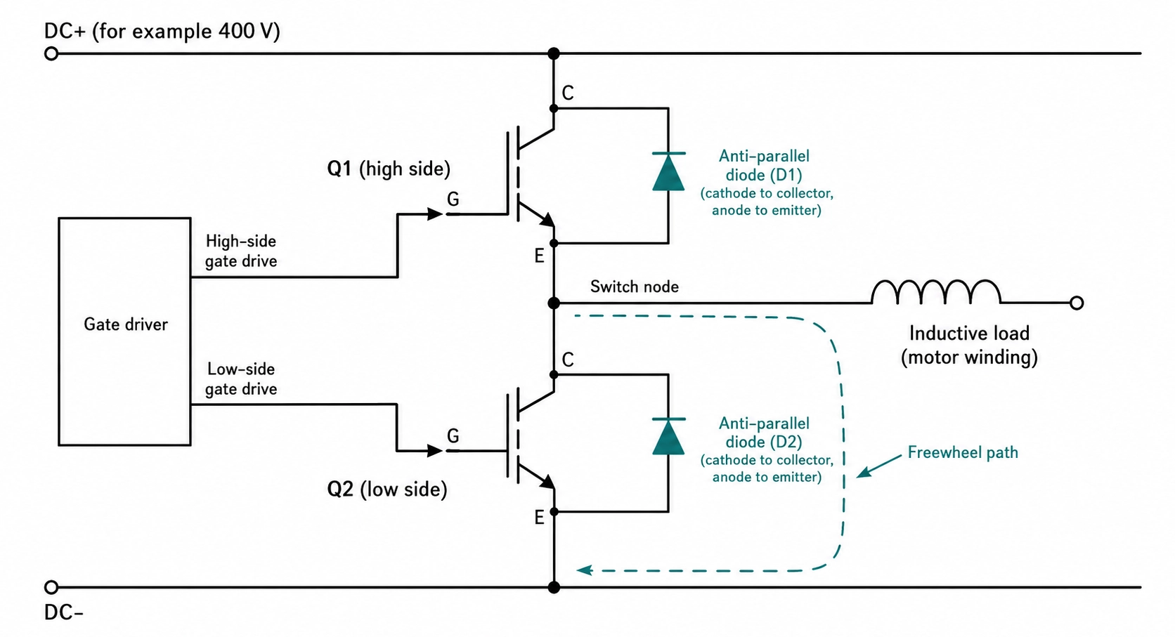
Figure: A two-IGBT half-bridge across a DC rail, with both gate drives
- Find the gap: Confirm the gate lead stops short of the conduction bar. A gap means you are applying a voltage, not sourcing base current.
- Follow the arrow: Pointing away from the body is N-channel. Both devices in Figure 9 are N-channel, which is normal for a half-bridge.
- Name the rails: The upper collector goes to the positive rail. Its emitter meets the lower collector, and that junction is the switch node.
- Check for a diode across C and E: Each device in Figure 9 has one, cathode to collector, so freewheel current from the load has a path in both switch states.
- Locate the gate reference: The low-side emitter sits at ground, so its VGE is straightforward. The high-side emitter rides on the switch node, which is why that driver needs a bootstrap or isolated supply.
- Confirm PINs against the datasheet: The symbol never states which physical pin is which.
The symbol tells you the emitter is the reference, and once that emitter swings between 0 V and the rail, a ground-referenced driver can no longer hold the device on.
Common Mistakes When Reading IGBT Symbols
- Reversing the emitter arrow: The drawing is not wrong; it is a different device, so no design rule check will flag it.
To fix this: on an N-channel part, the arrow points away from the body.
- Closing the gate gap: The symbol now reads as a bipolar base, and a reviewer may specify a base resistor for a device that needs a gate driver.
To fix this: leave the gate line clear of the conduction bar.
- Assuming an intrinsic body diode: A power MOSFET has one, and a standard IGBT does not, so an inductive load is left with no freewheel path.
To fix this: fit an external diode unless the datasheet shows a copack or an RC-IGBT.
- Calling the pins drain and source: The parts search then returns MOSFETs, and the gate drive gets specified against the wrong figures.
To fix this: the output stage is bipolar, so the terminals are collector and emitter.
- Trusting the symbol for pin order: KiCad alone ships eight N-channel IGBT symbols that differ in nothing but pin sequence.
To fix this: verify pin 1-2-3 against the package drawing before layout.
Conclusion
Rather than memorizing every IGBT symbol variant, use a consistent identification process: check the gap, then the arrow, then the diode, then the pin order. Those four checks separate an N-channel switch from a P-channel one, a copack part from a bare die, and a correct netlist from a swapped gate.
FAQs about IGBT symbols
Q: What do the three terminals on an IGBT symbol mean?
The gate (G) is the insulated control input and draws no meaningful steady current. The collector (C) is where the load current enters the device. The emitter (E) is where that current leaves, and it is also the reference point for the gate drive voltage.
Q: How do you tell an IGBT symbol from a MOSFET symbol?
An IGBT carries a single arrow on the emitter lead, while a MOSFET carries its arrow on the body lead entering the middle of the channel. The terminal letters confirm it: C and E for an IGBT, D and S for a MOSFET.
Q: Why does the IGBT symbol use collector and emitter instead of drain and source?
Because the output stage is a bipolar transistor, the PNP emitter inside the device serves as the IGBT collector, and the IGBT emitter corresponds to the source of the internal N-channel MOSFET. Terminal names follow the output half of the structure.
Q: Does every IGBT have a built-in freewheeling diode?
No. A standard IGBT has no intrinsic body diode, unlike a power MOSFET. Any anti-parallel diode is either a separate die co-packaged with the IGBT or an external component you fit yourself. Only the reverse-conducting IGBT integrates the diode on the same silicon.
Popular Articles
• Logic Gate Symbols: The Complete Chart, Truth Tables [2026]
• How to Design and Assemble a Reliable ESP32 Module PCB on a 2-Layer Board
• How to Identify SMD LED Polarity: Markings, Testing, and PCB Tips
• The Ultimate Guide to Relay Symbol: Coil, Contacts, Diagrams, and Circuit Applications
• Power Supply Symbols Chart: A Complete Guide to AC, DC, Ground, Battery, and Source Symbols
Keep Learning
How to Read Resistor Color Code: Complete Guide with Chart and Examples
4-Band Resistor Color Code Explained A 4-band resistor color code is one of the most common methods used to indicate resistance values in electronic components. It is widely used to help engineers and hobbyists quickly determine resistance values without using a resistor color code calculator. In a standard 4-band resistor: First Band (Digit 1): Represents the first significant digit Second Band (Digit 2): Represents the second significant digit Third Band (Multiplier): Indicates the factor by which t......
Solder Paste vs Flux: What's the Difference and When Should You Use Each?
Solder paste and flux are not interchangeable. Solder paste contains solder alloy powder and flux, while flux contains no solder alloy. This difference matters when choosing materials for SMT, reflow soldering, or manual soldering. Flux removes metal oxides and prevents re-oxidation, allowing molten solder to wet copper pads and component leads properly. Solder paste combines flux with fine solder alloy powder. During reflow, the flux activates to improve wetting while the solder alloy melts to form t......
Fiducial Marks in PCB and SMT Assembly: A Complete Guide to Accuracy and Design Rules
Modern Printed Circuit Boards (PCBs) are complex, integrating high-density components like 0.4mm pitch Ball Grid Arrays (BGAs), 0201 passives, and fine-pitch Quad Flat No-Lead (QFN) packages. In this advanced manufacturing environment, achieving placement accuracy measured in micrometers is crucial. A significant challenge in automated manufacturing is how pick-and-place machines, which handle thousands of components per hour, precisely locate the PCB. A board on a conveyor system is never in the perf......
Ground Symbols Explained: Earth, Chassis, Signal, Analog, Digital Ground & More
Key Takeaways ⬇ Download the Ground Symbol Cheat Sheet (PDF) Keep all six ground symbols and their standard numbers on one page for quick reference. Four IEC 60417 symbols: IEC 60417 defines symbol 5017 for earth, 5018 for functional earth, 5019 for protective earth, and 5020 for frame/chassis. Protective earth is safety-related: IEC 60417-5019 identifies the protective earth connection and is used for safety-related protective bonding. Signal ground uses a different convention: IEEE Std 315 defines t......
How to Choose an ESP32 Development Board: A Beginner-Friendly Guide
The leap from blinking a simple LED to building a cloud-connected smart home device is a thrilling milestone for any electronics beginner. At the heart of this transition is often one undisputed champion: the ESP32. However, when you first search for an ESP32 development board, you are instantly met with a dizzying array of models, shapes, and specifications. How do you know which one is right for your first IoT (Internet of Things) project? In this beginner's guide, we will break down what makes thes......
How to Design an ESP32-S3 Development Board from Scratch: A 4-Layer PCB Design Tutorial
Designing your own ESP32-S3 development board gives you complete control over your hardware architecture while preparing your IoT projects for commercial production. Instead of relying on bulkier, off-the-shelf boards, building a custom design allows you to optimize the board space, expose only the required GPIO pins, and integrate peripherals directly onto a single substrate. In this tutorial, we will design a 4-layer ESP32-S3 development board from scratch. We will walk through the entire hardware d......