
The Comprehensive Guide to Circuit Symbols: Key to Understanding Electrical and Electronic Diagrams
13 min
- Circuit Symbols Chart (Quick Reference)
- What Are Circuit Symbols?
- Common Circuit Symbols
- ANSI vs IEC Electrical Symbols
- How to Read a Circuit Diagram (Step by Step)
- Schematic Symbol vs PCB Footprint
- Common Mistakes When Reading Circuit Symbols
- FAQs about Circuit Symbols
Note
Need a quick reference while reading schematics?
Download our free, printable Circuit Symbols Cheat Sheet (PDF), featuring the most common IEC and ANSI symbols organized by category.
Keep it on your desktop or print it for easy reference at your workbench.
⬇ Download the Free Circuit Symbols Cheat Sheet (PDF)
Every electronic diagram is written in a visual language, and circuit symbols are its alphabet. From your first electrical schematic to a multi-layer board, knowing circuit symbols can make the difference between a drawing you can't read and one that you can easily understand.
This guide provides you with a full circuit symbols chart and a breakdown of each component commonly found in schematics.
Here we provide a breakdown of the differences among IEC, ANSI, and JIS standards, a step-by-step guide to reading a schematic, and a free, downloadable circuit symbols cheat sheet for your bench.
Circuit Symbols Chart (Quick Reference)
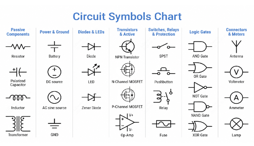
Figure: A quick-reference chart showing common circuit symbols
The table above is your one-screen circuit-symbol chart for the most common components in any schematic. You can jump straight to the different categories in this article, or grab the full cheat sheet from here.
The Ultimate Circuit Symbols Cheat Sheet [Free PDF Download] ⬇
| Component | Symbol (how it looks) | What it represents |
|---|---|---|
| Resistor | Zig-zag line (ANSI) or plain rectangle (IEC) | Limits current / drops voltage |
| Capacitor | Two parallel lines (one curved if polarized) | Stores charge, blocks DC, passes AC |
| Inductor | A row of loops/coils | Stores energy in a magnetic field |
| Battery | Alternating long and short parallel lines | DC voltage source |
| Ground | Three shrinking horizontal lines | 0 V reference/return path |
| Diode | Triangle pointing into a bar | Let's current flow one way only |
| LED | Diode with two arrows pointing outward | Emits light when forward-biased |
| NPN transistor | Circle with base bar and an arrow on the emitter (outward) | Current-controlled switch/amplifier |
| MOSFET | Gate, source, and drain with a channel line | Voltage-controlled switch/amplifier |
| Switch (SPST) | A break in the wire with a hinged lever | Opens or closes a connection |
| Fuse | Line through a small rectangle | Overcurrent protection |
| AND gate | Flat back, rounded (D-shaped) front | Output high only if all inputs are high |
| Voltmeter | Circle with a "V" inside | Measures voltage across two nodes |
| Wire junction | A solid dot where wires meet | Connected nodes (no dot = crossing only) |
What Are Circuit Symbols?
Circuit symbols are graphic shapes that represent electronic or electrical components in a schematic diagram in a standard way. Each symbol represents a part's function and the parts in which it connects, not necessarily what it actually looks like. Why is it so? Because in this way, engineers around the world can read the same circuit. In short, they turn a physical circuit into a clear, universal drawing.
Standards are important because a component may be depicted differently in different countries. A resistor is a zig-zag in the United States and a clean rectangle in Europe. Having one standard ensures your schematic is easy to read for manufacturers, collaborators, and reviewers. It prevents costly misreadings when your design moves from drawing to a finished PCB.
Common Circuit Symbols
Below are the symbols you will actually encounter, grouped into the categories that match how people read schematics. Under each group, you will find a short note on what the parts do.
Passive Components
Passive components are electronic components that cannot provide power gain. Instead, they store, dissipate, or transfer electrical energy without requiring an external power source for their basic operation.
Common passive components include resistors, capacitors, and inductors. These components form the foundation of many electronic circuits, including filters, timing networks, impedance matching networks, and biasing networks.
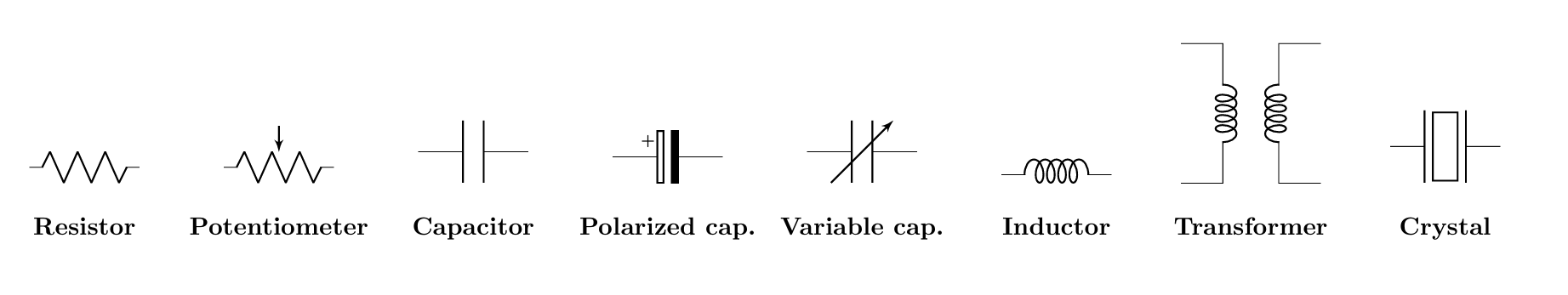
Figure: Circuit Symbols for Passive Components
| Component | Symbol (how it looks) | Function |
|---|---|---|
| Resistor | Zig-zag (ANSI) / rectangle (IEC) | Limits current, sets voltage levels |
| Potentiometer | Resistor with an arrow (wiper) across it | Adjustable resistance/voltage divider |
| Rheostat | Resistor with a diagonal arrow on one end | Variable resistance, two-terminal |
| Capacitor (non-polarized) | Two straight parallel plates | Stores charge, blocks DC, passes AC |
| Capacitor (polarized/electrolytic) | One straight plate, one curved plate, with a "+." | Polarity-sensitive bulk storage |
| Variable capacitor | Capacitor with an arrow through it | Tunable capacitance (RF tuning) |
| Inductor / Coil | A series of loops (ANSI) or a rectangle (IEC) | Stores energy magnetically, opposes current change |
| Transformer | Two coils facing each other with core lines between | Step the voltage up or down via magnetic coupling |
| Crystal / Resonator | A small rectangle between two capacitor-like plates | Sets a precise oscillation frequency |
Power & Ground
Power and ground symbols tell you where energy enters the circuit and where it returns. Getting these right is essential, as a misread ground reference is one of the most common beginner mistakes.
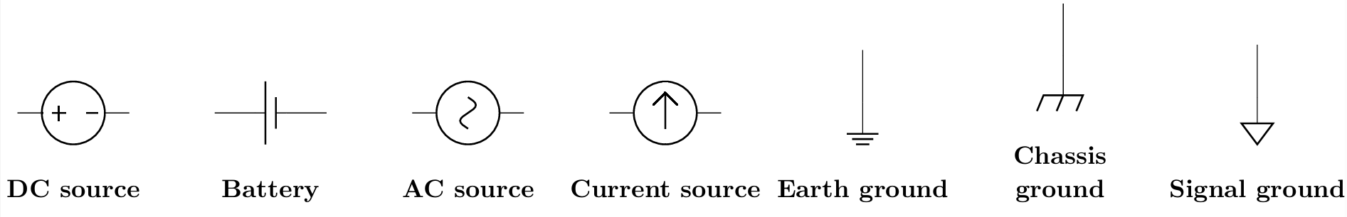
Figure: Circuit Symbols for power and ground
| Component | Symbol (how it looks) | Function |
|---|---|---|
| DC voltage source | Positive terminal (+) and negative (−) in a circle. | Constant DC supply (e.g., a cell) |
| Battery | Several alternating long/short lines stacked | Multi-cell DC source |
| AC source | A circle with a sine wave inside | Alternating current supply |
| Earth ground | Three horizontal lines shrinking downward | 0 V reference, earth connection |
| Chassis ground | A "rake" of angled hatching | Connection to the metal enclosure |
| Signal / common ground | A downward triangle | Common 0 V return for signals |
| VCC / V+ rail | An arrow or labeled node (VCC, +5V, +3V3) | Positive supply rail |
Diodes & LEDs
Diodes conduct current primarily in one direction while blocking reverse current. In schematic symbols, conventional current flows from the anode to the cathode when the diode is forward-biased. The vertical bar identifies the cathode, while an LED uses the same symbol with two outward arrows to indicate light emission.
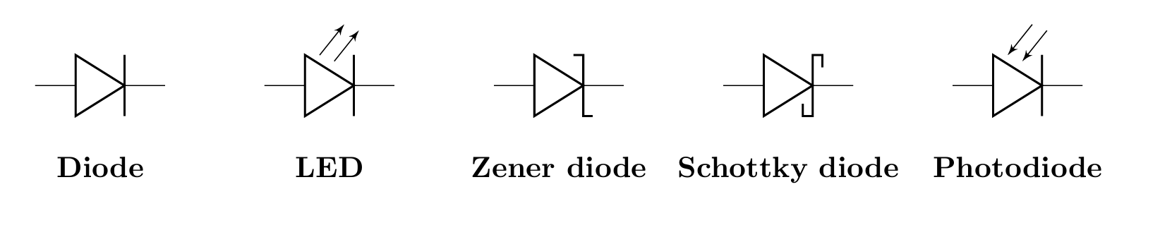
Figure: Diode symbol
| Component | Symbol (how it looks) | Function |
|---|---|---|
| Diode | Triangle pointing into a flat bar | Allows the current one-way (rectification) |
| LED | Diode with two arrows pointing away | Emits light when forward-biased |
| Zener diode | Diode with a bent, Z-shaped bar | Regulates voltage in reverse breakdown |
| Schottky diode | Diode with an S-shaped bar | Fast switching, low forward drop |
| Photodiode | A diode with two arrows pointing toward it | Converts light into current |
| Tunnel / Varactor diode | Diode with a curved or capacitor-like bar | Specialty RF/tuning use |
Transistors & Active Components
Active components use external energy to amplify or switch signals. Some of the best examples are transistors and op-amps. The key with transistors is the arrow, which marks the emitter (BJT) and shows current direction.
Figure: Circuit Symbols for Active Components
| Component | Symbol (how it looks) | Function |
|---|---|---|
| NPN transistor (BJT) | Base bar; emitter arrow points outward | Switch/amplifier, current flows in on the collector |
| PNP transistor (BJT) | Base bar; emitter arrow points inward | Switch/amplifier, complementary to NPN |
| N-channel MOSFET | Gate, source, drain; arrow points inward | Voltage-controlled switch (logic, power) |
| P-channel MOSFET | Gate, source, drain; arrow points outward | Complementary MOSFET switch |
| JFET | Gate joins a channel line with an arrow | Voltage-controlled, high input impedance |
| Operational amplifier | A triangle with + and − inputs | Amplifies the difference between two inputs |
| Integrated circuit (IC) | A rectangle with numbered pins | A packaged sub-circuit (MCU, regulator, etc.) |
Switches, Relays & Protection
These parts are normally acting switches that can open and close in order to protect or turn on/off a circuit. Switches and relays make and break connections, and fuses, on the other hand, burn against an overcurrent.
Figure: Switch symbols
Figure: Relay and Protection Symbols
| Component | Symbol (how it looks) | Function |
|---|---|---|
| Switch (SPST) | A hinged lever breaks the wire | Single on/off contact |
| Switch (SPDT) | A lever that swings between two contacts | Selects one of two paths |
| Pushbutton (NO) | A button bridging two contacts | Momentarily make contact |
| Relay | A coil next to a switch contact | The coil energizes to move the contact |
| Fuse | A line through a small rectangle (or "S" shape) | Breaks the circuit on overcurrent |
| Circuit breaker | A switch with an "x" or a break box | Resettable overcurrent protection |
Logic Gates
Logic gates are the building blocks of digital circuits; they are internally based on a number of transistors coming together in a certain order. Their ANSI/IEEE shapes are the most recognizable symbols in electronics. You should learn at least these five, and you can read most digital schematics.
Figure: Logic gate symbols
| Gate | Symbol (how it looks) | Logic function |
|---|---|---|
| Buffer | A plain triangle | Output equals input |
| NOT (Inverter) | Triangle with a small bubble on the tip | Output is the inverse of input |
| AND | Flat back, rounded (D-shaped) front | High only if all inputs are high |
| OR | Curved back, pointed front | High if any input is high |
| NAND | AND shape with an output bubble | Inverted AND |
| NOR | OR shape with an output bubble | Inverted OR |
| XOR | OR shape with an extra curved back line | High if inputs differ |
Connectors & Meters
Finally, connectors bring signals on and off the board, and meters let you measure what is happening at a node.
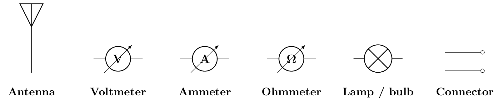
Figure: Connector and meter symbols
| Component | Symbol (how it looks) | Function |
|---|---|---|
| Connector / Header | Pins or a labeled box | Off-board input/output point |
| Antenna | A small "T" or triangle on a stem | Transmits/receives RF |
| Voltmeter | A circle with "V" | Measures voltage across two points |
| Ammeter | A circle with "A" | Measures current through a wire |
| Ohmmeter | A circle with "Ω." | Measures resistance |
| Lamp / Bulb | A circle with an "x" or a loop inside | Indicator or load |
| Speaker / Buzzer | A trapezoid or coil-and-arc shape | Converts a signal to sound |
ANSI vs IEC Electrical Symbols
Three main rules dictate the way in which circuit symbols are drawn, and the symbol you use will depend upon where your audience is.
- The ANSI / IEEE (Y32.2 / Std 315) standard is adopted in the United States and some parts of Asia. It is more pictorial and descriptive in shape.
- IEC 60617 is the international standard, however, which is predominant in Europe and is now gaining dominance globally. It uses simple, language-independent shapes and labels the references (e.g., "R1").
The gap is most obvious between the resistor and the inductor. Let's do a comparison side by side:
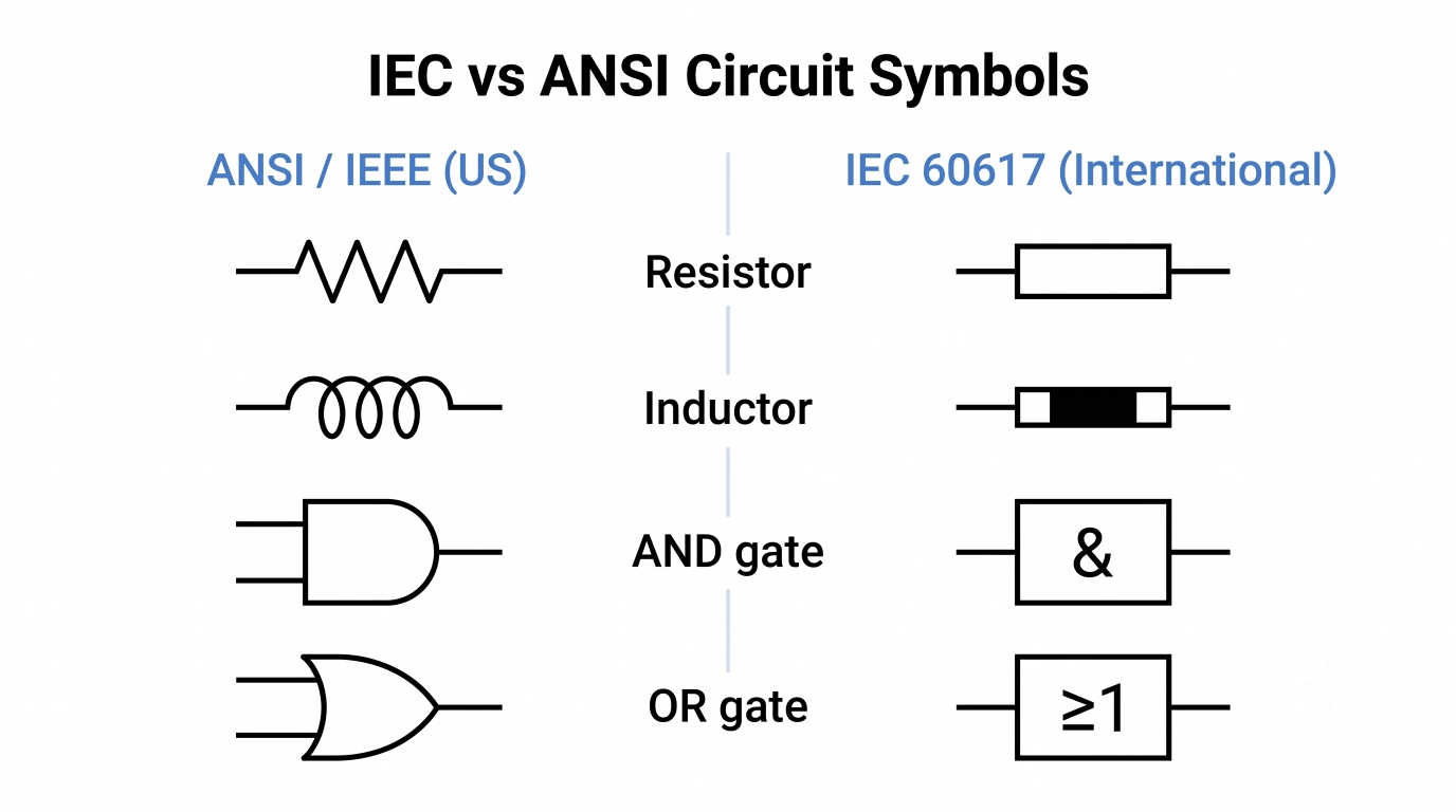
Figure: IEC vs ANSI circuit symbols for the resistor and the logic gates.
| Component | ANSI / IEEE | IEC 60617 (and JIS) |
|---|---|---|
| Resistor | Zig-zag line | Plain rectangle |
| Inductor | A row of looped coils | A narrow rectangle (or filled bar) |
| Fuse | Line through an oval/rectangle | A rectangle with a line through the center |
| Logic gates | Distinctive shapes (D-shape AND, etc.) | Rectangular boxes with "&", "≥1", as labels |
How to Read a Circuit Diagram (Step by Step)
Once you know the symbols, reading a schematic is a repeatable process.
Note
For a more detailed, step-by-step walkthrough, read our complete guide to understanding electrical schematics.
- Find power and ground first. Locate the supply rail (VCC, +5V) at the top and ground at the bottom. Current conceptually flows from the higher potential down to ground.
- Identify the main building blocks. Scan for ICs, transistors, and connectors; these are the "verbs" of the circuit that do the work.
- Trace the signal path left to right. Most schematics are drawn with inputs on the left and outputs on the right. Follow the wires from source to load.
- Read the wire junctions carefully. A solid dot means the wires are connected; a plain crossing (or a little hop) means they are not.
- Note the reference designators and values. R1 = 10 kΩ, C3 = 100 nF. These labels tell you exactly which part each symbol is.
- Group the functional stages. Recognize sub-circuits, a power supply section, an amplifier stage, and a microcontroller block, and read each as a unit.
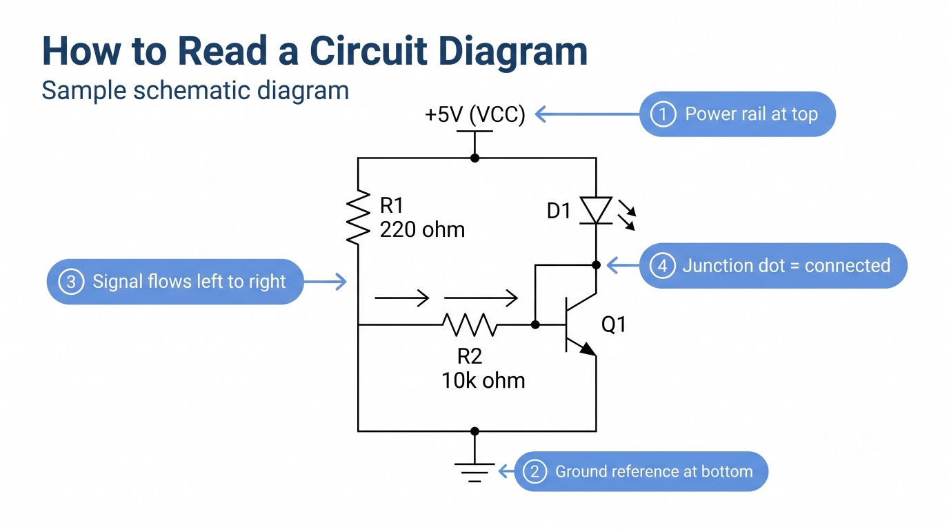
Figure: One sample schematic showing power rail, ground, signal path, and labeled reference
Schematic Symbol vs PCB Footprint
A circuit symbol and a PCB footprint represent the same component in two different worlds. Let’s see how:
- The schematic symbol is the logical view. It shows the component's function and its electrical connections. For example, a resistor is a simple zig-zag or rectangle with two terminals. It says nothing about the part's real size.
- The PCB footprint (or land pattern) is the physical view. It is the exact arrangement of copper pads, drill holes, and silkscreen that the real part is soldered onto. For example, a 0402 or 0805 surface-mount resistor land pattern with precise pad dimensions.
In your EDA tool, every schematic symbol is mapped to a footprint before layout. Getting that mapping wrong means the board will not assemble correctly, even though the schematic looks perfect. That is why the symbol-to-footprint link is one of the most important steps in PCB design.
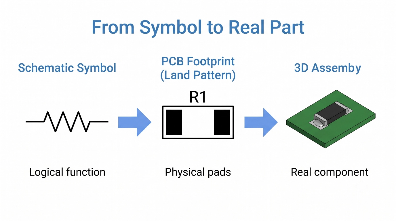
Figure: Schematic symbol → PCB footprint → 3D assembly workflow.

- After verifying your symbols and footprints, it's time to bring your design to life.
- Simply upload your Gerber files to JLCPCB for an instant PCB fabrication quote.
Need PCB assembly too? Import your BOM and Pick & Place files, source components from the JLCPCB Parts Library, and receive professionally assembled PCBs delivered to your door.
Common Mistakes When Reading Circuit Symbols
Even experienced builders trip on these. Watch out for:
- Ignoring polarity: Electrolytic capacitors, diodes, and LEDs only work one way.
- Misreading wire crossings: A junction dot is mandatory for a real connection.
- Confusing NPN and PNP (or N- and P-channel): The arrow direction is the only clue, and it changes the whole circuit's behavior.
- Overlooking the ground reference: Earth, chassis, and signal grounds are different symbols and sometimes different nets.
FAQs about Circuit Symbols
Q: What are the most common circuit symbols?
The ones that you will be seeing in almost every schematic are: resistor, capacitor, inductor, diode, LED, transistor, battery, ground, switch, and the basic logic gates (AND, OR, NOT). Know these and read most beginner and intermediate circuits.
Q: What are the differences between IEC and ANSI circuit symbols?
ANSI (US) symbols are more pictorial; a resistor is a zig-zag, and logic gates have distinctive shapes. The IEC (international) symbols are easier and do not carry any language: a resistor is a simple rectangle, logic gates are boxes with "&" or "≥1. The Japanese standard JIS is harmonized with IEC, thus they are similar in nature.
Q: How to determine if two wires are connected in a schematic?
Find a solid dot at the crossing point. A dot represents an electrical connection (a node), and a crossing with no dot, or a small "hop" arc, represents a crossing with no electrical connection.
Q: Are circuit symbols and PCB footprints the same?
No. The circuit symbol is the symbolic representation of the part that is used in your schematic, and the footprint (land pattern) is the actual copper pattern that the actual part will be soldered onto. Before laying out the board, each symbol is mapped to a footprint.
Popular Articles
• Understanding Electrical Schematics: A Comprehensive Guide
• The Comprehensive Guide to Circuit Symbols: Key to Understanding Electrical and Electronic Diagrams
• PCB Board Design: A Step-by-Step Guide for Beginners
• Choosing the Best PCB Color-Enhancing Aesthetics and Functionality
• PCB Silkscreen: All You Need to Know
Keep Learning
Understanding Electrical Schematics: A Comprehensive Guide
Key Takeaways Schematics vs. Block Diagrams: Schematics detail exact components and connections; block diagrams only show high-level functions. Mark Polarity: Essential to prevent circuit failure and automated SMT placement errors at JLCPCB. Clean Layout: Use modular blocks and net labels (VIN, GND) to eliminate visual clutter. Manufacturing Ready: Follow DFM trace rules and export standard Gerber, BOM (LCSC C-IDs), and CPL files. Fast Troubleshooting: Isolate schematic blocks to test expected voltage......
A Beginner's Guide to Basic Electronic Components: Functions, Symbols & Uses
Every circuit, from a simple LED flashlight to a microcontroller board, is built from the same handful of common electronic components. This guide breaks down the ten basic electronic components you will encounter most often: What each component does How it works Key specifications Where engineers use it By the end, you will be able to recognize these electronic circuit components on a schematic, a PCB, or a parts bin, and know exactly why each one is there. These electronic components are the buildin......
Via Stubs in High-Speed PCB Design: Causes, Effects, and Solutions
Key Takeaways Via stubs are unused via sections that cause reflections, resonance, and jitter in high-speed PCBs. They become critical above 5–10 Gbps; stubs longer than 15 mils (0.381 mm) need mitigation. JLCPCB precision back-drilling reduces residual stubs to under 0.15 mm, greatly improving signal integrity. Optimized stack-up and back-drilling offer the best balance of performance and cost versus blind/buried vias. Choose experienced manufacturers like JLCPCB for reliable high-speed PCB fabricati......
The Comprehensive Guide to Circuit Symbols: Key to Understanding Electrical and Electronic Diagrams
Note Need a quick reference while reading schematics? Download our free, printable Circuit Symbols Cheat Sheet (PDF), featuring the most common IEC and ANSI symbols organized by category. Keep it on your desktop or print it for easy reference at your workbench. ⬇ Download the Free Circuit Symbols Cheat Sheet (PDF) Every electronic diagram is written in a visual language, and circuit symbols are its alphabet. From your first electrical schematic to a multi-layer board, knowing circuit symbols can make ......
Hierarchical Design : Making Complex PCB Projects More Manageable
Key Takeaway Hierarchical design transforms complex PCB projects from overwhelming single-sheet nightmares into well-organized, modular, and manageable systems. By breaking down large schematics into functional blocks with clear interfaces, engineers can significantly improve organization, reduce errors, enhance reusability, and enable smoother collaboration. This approach not only simplifies debugging and layout but also leads to better DFM outcomes and faster time-to-market, making it the preferred ......
Why a Clean PCB Netlist Is the Foundation of Successful Manufacturing
Key Takeaways A clean PCB netlist is the foundation of successful manufacturing, serving as the single source of truth that bridges schematic and physical PCB layout. By ensuring accurate component data, net connections, and version control, it prevents costly errors, improves yield, and enables reliable production. Mastering IPC-D-356 netlist best practices helps engineers reduce risks and achieve high-quality results with JLCPCB. Ever wonder what exactly the link is between your wonderfully drawn sc......