How Hierarchical Schematic Design Simplifies Complex PCB Layouts and Streamlines Manufacturing
13 min
- Introduction to Hierarchical Schematic Design
- Key Benefits of Using Hierarchical Schematics in PCB Design
- Step-by-Step Guide: How to Structure a Hierarchical Schematic
- Common Pitfalls in Hierarchical Design and How to Avoid Them
- From Hierarchical Schematic to Flawless Fabrication with JLCPCB
- FAQ about Hierarchical Schematic Design
Key Takeaways
- A hierarchical schematic organizes complex circuits into top-level block symbols linked to nested sub-sheets, replacing flat, hard-to-navigate drawings.
- Hierarchical design cuts human error, enables parallel team development, and makes validated sub-circuits reusable across projects.
- Follow a four-step workflow: map top-level blocks, define port directions, manage net scope, then translate sheets into PCB layout.
- Watch for net-scope conflicts and duplicate BOM designators when sub-sheets are duplicated across a design.
- JLCPCB supports hierarchical projects end to end, from EasyEDA capture to 2–32 layer fabrication and SMT assembly.
Introduction to Hierarchical Schematic Design
A hierarchical schematic structures complex electronic designs by organizing circuits into top-level functional blocks and nested sub-sheets rather than spreading them across flat, disconnected drawings. This architectural approach is essential for managing dense modern hardware, preventing signal routing mistakes, and ensuring error-free multi-layer PCB fabrication.
What is a Hierarchical Schematic?
A hierarchical schematic is a structural circuit design methodology where the top level of a project acts as an interactive functional block diagram. Instead of placing hundreds of individual component symbols across multiple unorganized pages—known as a flat schematic—a hierarchical workflow relies on strict parent-child relationships. Top-level sheet symbols represent major subsystem blocks (such as Power Management, MCU, or Audio DSP), and each block links directly to an underlying sub-sheet containing the specific components and internal wiring.
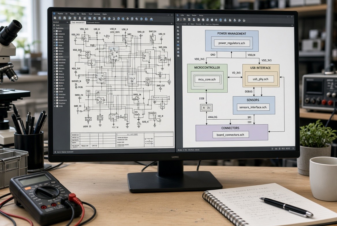
Signals traverse between parent and child sheets using explicitly defined hierarchical ports and pins. By treating complex sub-circuits as self-contained functional units, engineers can navigate, review, and maintain high-density board projects without losing visual context. To understand how flat and hierarchical architectures differ during daily engineering tasks, consider the structural comparisons below:
-
Sheet Relationship
All schematic sheets exist on a single horizontal plane without structural nesting.
-
Inter-Sheet Routing
Relies heavily on global net labels (e.g., VCC_5V, UART_TX) distributed across dozens of pages.
-
Visual Traversal
Engineers must manually scan multiple pages to trace signal pathways across sub-systems.
-
Scalability
Best suited for simple, low-component-count designs (under 100 components).
-
Sheet Relationship
Organized in a top-down tree hierarchy with parent sheet blocks linked to child sub-sheets.
-
Inter-Sheet Routing
Uses explicit hierarchical ports and sheet pins to control net visibility and scope strictly.
-
Visual Traversal
Navigated instantly by double-clicking block symbols to enter sub-circuit schematics.
-
Scalability
Designed specifically for high-density, enterprise-level PCB projects (hundreds or thousands of components).
Why Modern Complex Hardware Requires Hierarchical Structuring
Modern electronic design demands high-speed digital architectures and multi-layer stackups that make flat schematic capture rapidly unmanageable. When designs exceed hundreds of components, flat multi-sheet schematics rely heavily on global net labels, which significantly increase the risk of accidental signal shorts, make cross-sheet tracking tedious, and obscure main signal paths.
Adopting a hierarchical schematic methodology directly solves these scalability issues through four core design pillars:
- Signal Scope Isolation: Net connections remain localized inside individual sub-sheets by default, preventing unwanted inter-sheet signal collisions.
- Early Constraint Management: High-speed interfaces (such as PCIe, DDR memory, or USB 3.0) are grouped into isolated modules upfront, making it easier to apply differential pair matching and controlled impedance rules early in the design cycle.
- Streamlined Code and Hardware Co-Design: Embedded software engineers can read top-level hardware blocks like code libraries, correlating MCU GPIO allocation directly to specific functional block sheets.
- Enhanced Design Review Workflows: Peer reviewers can evaluate high-level system logic at the parent sheet level before diving into component-level sub-sheets, dramatically reducing engineering audit times.
Key Benefits of Using Hierarchical Schematics in PCB Design
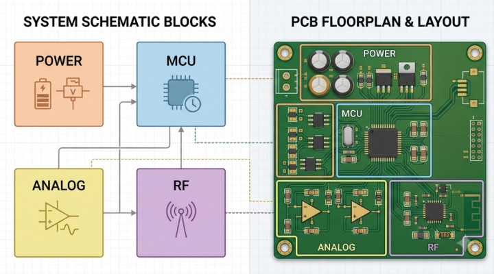
Implementing hierarchical schematic structures provides engineering teams with modular reusability, seamless parallel development, and fewer netlist errors. These benefits directly reduce engineering cycle times and translate to higher manufacturing yields during prototype and volume production runs.
Design Reusability and Modular Engineering
Building hardware with a hierarchical schematic approach converts individual circuit functions into standardized engineering modules. Once a multi-phase buck converter, USB-C interface, or micro-controller pinout is fully validated in lab testing, its underlying sub-sheet can be saved and reused across multiple projects without redesigning the circuit from scratch.
Modular design reduces engineering hours while improving hardware reliability. Pre-tested hierarchical sub-sheets carry proven layout rules and component footprints directly into new designs, eliminating recurring design-for-manufacturability (DFM) errors during production.
Faster Team Collaboration and Parallel Development
In multi-engineer hardware teams, flat schematics create severe version-control bottlenecks because engineers cannot work inside the same project file simultaneously without file corruption or merge conflicts. A hierarchical schematic solves this by breaking the system into discrete sub-sheet files that can be version-controlled independently.
Hardware team leads can divide tasks across specialized engineers seamlessly:
- RF & Wireless Specialist: Optimizes the Bluetooth/Wi-Fi front-end circuitry on sub-sheet RF_FrontEnd.sch.
- Power Electronics Engineer: Refines high-efficiency switched-mode power supplies on sub-sheet Power_Supply.sch.
- Analog & Sensor Engineer: Calibrates high-precision analog signal conditioning on sub-sheet Sensor_Array.sch.
- Lead System Architect: Links all completed sub-sheets on the master top-sheet using standardized hierarchical ports and runs project-level ERC checks.
Reduced Human Error and Easier Debugging
Electrical errors—such as duplicate net labels, floating input pins, and accidental short circuits—are common causes of costly board revisions. A hierarchical schematic confines signal nets to local scopes unless they are explicitly routed out through hierarchical ports.
This strict scope containment isolates signal paths, preventing accidental inter-sheet net collisions. If a signal anomaly occurs during physical board bringing-up, engineers can trace the fault directly back to a specific functional block symbol rather than searching through dozens of unstructured schematic pages.
Step-by-Step Guide: How to Structure a Hierarchical Schematic
Structuring an effective hierarchical schematic requires mapping top-level block symbols, defining pin directions accurately, and managing net scopes before forward-annotating to PCB layout. Following standard engineering rules ensures a smooth transition from logical capture to physical layout and netlist extraction.
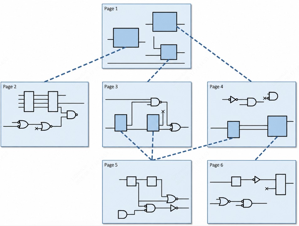
Step 1: Mapping Top-Level Block Diagrams and Sheet Symbols
Begin by creating the master sheet in your EDA environment (such as EasyEDA, Altium, or KiCad). Instead of drawing component symbols immediately, place high-level Sheet Symbols to represent core hardware sub-systems.
Arrange these block symbols logically to reflect physical signal and power flow: power inputs on the left, core processing in the middle, and peripheral interfaces or analog outputs on the right. Each sheet symbol links directly to a target child sub-sheet file.
Step 2: Defining Port Connections and Hierarchical Pins
After instantiating sheet symbols on the parent page, place Hierarchical Ports inside each child sub-sheet to define signals entering or exiting the module. Synchronize these sub-sheet ports with the parent sheet symbol to create corresponding Hierarchical Pins.
Always explicitly specify pin electrical types during creation to maximize EDA validation engine efficiency:
- Input Ports: Reserved for incoming control lines, clock sources, and sensor feedback signals.
- Output Ports: Assigned to driven output drivers, status indicators, and analog signals.
- Bidirectional Ports: Essential for multi-drop communication buses like I2C_SDA, CAN_H/CAN_L, and memory data lines.
- Power Ports: Designated for system power rails (+3V3, +5V, VBUS) and reference grounds (GND, AGND).
Correct pin definitions allow your EDA software's Electrical Rules Check (ERC) tool to catch floating nets, mismatched pin types, and undriven logic lines before generating the physical board netlist.
Step 3: Managing Net Names, Buses, and Power Planes Across Sheets
Managing net scope is critical in multi-sheet schematic design. Local nets stay contained inside their respective sub-sheet, whereas bus signals (such as SPI_MOSI, UART_TX, or I2C_SDA) connect across blocks through defined hierarchical ports.
For power distribution, engineers must choose the appropriate scope strategy based on circuit sensitivity:
- Global Power Nets: Standard power names (like GND or +3V3) automatically pass through all schematic sheets. This reduces visual clutter but requires strict discipline to prevent noisy digital power from entering sensitive analog domains.
- Hierarchical Power Ports: Power rails are explicitly routed through sheet ports (e.g., AVCC_3V3 or AGND). This provides complete isolation, allowing engineers to implement ferrite bead filtering and single-point ground ties at specific top-level locations.
Step 4: Translating Sheet Blocks to PCB Layout Packaging
Once the schematic passes the Electrical Rules Check (ERC), extract the hierarchical netlist to initialize physical PCB layout. Modern EDA software allows you to map schematic sheet structures directly into physical layout Rooms or Component Clusters.
Grouping physical components on the board according to their schematic sub-sheets simplifies placement. High-speed traces, power decoupling caps, and ESD protection arrays remain located immediately next to their associated IC pins, preserving signal integrity before main bus routing begins.
Common Pitfalls in Hierarchical Design and How to Avoid Them
Errors in a hierarchical schematic usually stem from misconfigured net scopes, component re-annotation conflicts, and unverified netlists. Identifying these issues early prevents manufacturing delays, assembly rework, and bare-board scrap.
Mismatched Net Scope and Global/Local Signal Confusion
A frequent error in hierarchical schematic capture is mixing global and local net scopes without intention. If an engineer places a local net label on a child sheet and reuses that same label name on another sheet—assuming it stays local—some EDA tools may merge those nets globally, causing unintentional short circuits.
To prevent net scope conflicts, adopt a standardized three-tier naming convention across all engineering files.
Duplicate Designators During BOM Generation
When hierarchical sub-sheets are duplicated across a design (for instance, four identical channels of an audio driver), component designators (e.g., R1, C1, U1) inside those sub-sheets can conflict during Bill of Materials (BOM) export.
Prevent duplicate designators by configuring your EDA tool's automatic multi-sheet annotation rules. Use naming formats such as R_Sheet1_1 or assign distinct designator offset ranges (such as R100 series for Sheet 1, R200 series for Sheet 2, and R300 series for Sheet 3). This guarantees accurate component placement during automated SMT assembly.
DFM and Netlist Verification Before PCB Order
Generating Gerber or ODB++ fabrication files without validating the netlist is a major cause of manufacturing failures. A schematic visual drawing can look correct while containing broken electrical connections inside the background netlist.
Before submitting design files for manufacturing, follow this essential pre-flight checklist:
- Run Electrical Rules Check (ERC): Ensure 0 errors and 0 unacknowledged warnings for floating pins or undriven nets.
- Export IPC-D-356 Netlist: Generate a standardized electrical netlist directly from your compiled schematic.
- Cross-Verify Gerber Netlist: Use a DFM viewer to compare your Gerber copper layout against the exported IPC-D-356 netlist.
- Audit Multi-Sheet BOM: Verify that all channels in duplicated sub-sheets have unique designators and assigned manufacturer part numbers (MPNs).
From Hierarchical Schematic to Flawless Fabrication with JLCPCB
JLCPCB turns complex hierarchical schematic designs into physical hardware through native EasyEDA integration, automated netlist validation, and advanced multi-layer manufacturing capabilities. This end-to-end integration bridges logical schematic design directly to precision board fabrication and assembly.

Seamless EDA Integration with EasyEDA and Major CAD Tools
Engineers using EasyEDA can capture hierarchical multi-sheet schematics and transfer them directly into the JLCPCB ordering system with a single click. EasyEDA natively formats component reference designators, BOM data, and netlist files to match JLCPCB's fabrication parameters seamlessly.
For engineers working in external EDA environments such as Altium Designer, KiCad, or OrCAD, JLCPCB supports standard manufacturing exports. Submitting a clean IPC-D-356 netlist generated from your hierarchical project enables automated parsing and faster production turnaround.
Automated Netlist and DFM Rule Checking at Ordering Stage
When you upload your project files to JLCPCB, an automated Design for Manufacturability (DFM) engine evaluates your board geometry against physical fabrication limits. The system checks trace widths, clearances, hole aspect ratios, and copper layer symmetry to identify potential production defects prior to etching.
Rapid Prototyping for High-Density and Multi-Layer Designs
Translating a multi-sheet hierarchical schematic into a dense multi-layer PCB requires high-precision manufacturing processes. JLCPCB supports production runs from 2 to 32 layers using High-Tg FR-4 materials, tight trace impedance tolerances (±10%), and advanced surface finishes such as Electroless Nickel Immersion Gold (ENIG).
Combining JLCPCB's bare-board fabrication with their turnkey SMT Assembly Service allows engineers to submit hierarchical BOM and CPL (Component Placement Location) files for automated assembly. By cross-checking netlists against physical assembly files, JLCPCB eliminates manual soldering errors, delivering fully assembled, production-ready boards in as fast as 24 to 48 hours.
| Process Parameter | Standard Capabilities (4 - 6 Layers) | High-Layer Line (8 - 32 Layers) | Engineering Significance |
|---|---|---|---|
| Max Layer Count | Up to 6 Layers | Up to 32 Layers | Accommodates ultra-dense hierarchical signal routing. |
| Min Trace / Clearance | 3.5 / 3.5 mil (0.09mm) | 3.0 / 3.0 mil (0.076mm) | Enables tight BGA fanouts and controlled impedance routing. |
| Min Mechanical Drill | 0.20 mm | 0.15 mm | Reduces via pad footprints and maximizes routing channels. |
| Via Surface Treatment | Tented / Exposed | Resin Plugged & Capped (POFV) | Essential for Via-in-Pad fine-pitch component placement. |
| Surface Finish Options | HASL, Lead-Free HASL, ENIG | ENIG Standard | Ensures flat pad surfaces for reliable SMT component soldering. |
FAQ about Hierarchical Schematic Design
Q: What is the difference between a flat schematic and a hierarchical schematic?
A flat schematic places all components on a single horizontal plane and relies on global net labels for inter-sheet connections. A hierarchical schematic organizes circuits into parent block symbols linked to nested child sub-sheets, using hierarchical ports and sheet pins to control net scope.
Q: When should I use a hierarchical schematic instead of a flat schematic?
Use a hierarchical schematic when your design exceeds roughly 100 components or involves high-speed interfaces, multiple functional blocks, or multi-engineer collaboration. Flat schematics remain sufficient for simple, low-component-count boards.
Q: How do hierarchical ports and sheet pins work?
Hierarchical ports placed inside a child sub-sheet define the signals entering or exiting that module. Synchronizing these ports with the parent sheet symbol creates corresponding sheet pins, so signals can only cross sheet boundaries through explicitly defined connections.
Q: Can hierarchical sub-sheets be reused across different projects?
Yes. Once a sub-sheet (such as a power supply or USB-C interface) is validated in testing, it can be saved and reused across projects, carrying proven layout rules and component footprints into new designs.
Q: Does JLCPCB support hierarchical schematic designs?
Yes. JLCPCB integrates natively with EasyEDA for hierarchical multi-sheet capture and accepts standard IPC-D-356 netlists from Altium, KiCad, and OrCAD, with automated DFM checking and 2-32 layer fabrication.
Conclusion on Hierarchical Schematic Design
Hierarchical schematic design transforms complex, high-density PCB projects into organized, reusable, and easily reviewable subsystems. By structuring circuits into top-level block symbols linked to nested sub-sheets, engineering teams reduce netlist errors, accelerate parallel development, and streamline the path from logical capture to physical fabrication. Pairing this methodology with JLCPCB's EasyEDA integration and automated DFM checks delivers error-free boards from prototype through volume production.
Popular Articles
• The Comprehensive Guide to Circuit Symbols: Key to Understanding Electrical and Electronic Diagrams
• Design Guidelines for PCB Using FR4 Substrates
• Choosing the Best PCB Color-Enhancing Aesthetics and Functionality
• PCB Silkscreen: All You Need to Know
• PCB Board Design: A Step-by-Step Guide for Beginners
Keep Learning
How to Read and Create PCB Schematics
Key Takeaways Read Schematics: Understand symbols, net labels, and component values. Design in EasyEDA: Place components and create circuit connections. Run Design Checks: Use ERC and DRC to identify potential issues. Verify Components: Check pin assignments and PCB footprints. Prepare for Manufacturing: Validate PCB layouts and manufacturing files. Printed circuit board (PCB) design begins with a clear understanding of how the electronic circuit should function. A schematic diagram represents the cir......
Maximizing Circuit Reliability with PCB Test Points and Smart DFT
Key Takeaways Early Fault Catching: Test points drastically reduce diagnosis time and prevent costly field failures. Standard Pad Sizing: Use 1.0 mm flat copper pads with 2.54 mm spacing for optimal fixture contact. Protect High-Speed Signals: Keep branch traces short to prevent capacitive loading and resonance. Single-Sided Access: Place all test pads on the bottom layer to cut fixture costs. Right Test for Volume: Use flying probe for prototypes and bed-of-nails ICT for mass production. A PCB test p......
The Comprehensive Guide to Circuit Symbols: Key to Understanding Electrical and Electronic Diagrams
Note Need a quick reference while reading schematics? Download our free, printable Circuit Symbols Cheat Sheet (PDF), featuring the most common IEC and ANSI symbols organized by category. Keep it on your desktop or print it for easy reference at your workbench. ⬇ Download the Free Circuit Symbols Cheat Sheet (PDF) Every electronic diagram is written in a visual language, and circuit symbols are its alphabet. From your first electrical schematic to a multi-layer board, knowing circuit symbols can make ......
Design Guidelines for PCB Using FR4 Substrates
Material substrate concerns are necessary while designing electrical circuit boards. This is due to the fact that printed circuit boards cannot be manufactured without the appropriate PCB materials. When developing and producing circuit boards, the substrate material must be taken into account just as much as the copper layers, silkscreen, and surface polish. Generally speaking, non-conductive materials like porcelain, Marlon, FR4, and the like must be used for PCB substrates. Depending on its intende......
Choosing the Best PCB Color-Enhancing Aesthetics and Functionality
Key Takeaways Choosing the best PCB solder mask color involves balancing aesthetics, visibility, and functionality. Green remains the top choice for superior contrast and inspection, while black offers premium appeal, white excels in LED applications, and other colors like purple and red provide unique design options. The ideal color depends on your priorities in inspection ease, thermal performance, and brand image, with minimal impact on electrical performance when using proper silkscreen contrast. ......
4 Layer vs 6 Layer vs 8 Layer PCB: How to Choose the Right Stackup
Random selection of layers in electronics may lead to serious signal integrity issues. That's why we always design our stackup before designing the PCB. Stackup decides the type of PCB and how it gonna perform under high-frequency conditions. There are a lot of things that directly affect the stackup of the PCB, related to impedance matching, routing density, signal and power integrity, electromagnetic compatibility (EMC), and cost. Knowing the requirements before design and the most critical componen......