
PCB Silkscreen: All You Need to Know
11 min
- What is a PCB Silk Screen?
- Different Methods to Create PCB Silkscreens:
- The Traditional PCB Screen Printing Process:
- JLCPCB Manufacturing Notes & DFM Capabilities:
- FAQ about PCB Silkscreen
- Conclusion
Key Takeaways
The PCB Silkscreen Guide demonstrates that a properly designed legend layer is essential to prevent assembly failures and ensure long-term hardware reliability. By mastering modern manufacturing methodologies like Direct Legend Printing (DLP) and aligning layouts with JLCPCB's strict DFM design rules—including the absolute 0.8 mm character height limit and the automated 0.15 mm silkscreen clipping protocol driven by solder mask precedence—engineers can seamlessly eliminate cold joints and optimize their boards for flawless production.
Silkscreen is the topmost layer of a PCB, adding a silkscreen layer is the final step in PCB manufacturing. This layer adds ink markings to identify PCB components, test points, symbols, logos, and other important details. Silkscreen plays a crucial role in helping manufacturers and designers easily identify components by annotating them on PCB.
The silkscreen ink is a specially non-conductive formulated epoxy. It comes in various colors, the most common in the industry are black and white. PCB design software typically uses standard fonts for silkscreen layers, though designers have the flexibility to choose other fonts as needed. In this article, we’ll explore the importance of silkscreen, design guidelines, useful tips and tricks, and how to incorporate custom fonts into the silkscreen layer. See the full comprehensive guide, how PCB are manufactured in JLCPCB fab.
What is a PCB Silk Screen?
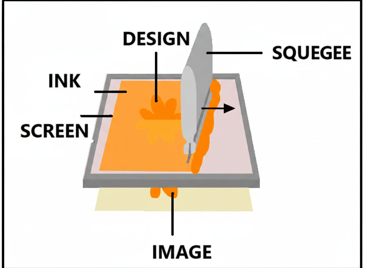
Think of roads and streets that lack direction/distance texts and landmarks. Do they make any sense? Similarly a PCB silkscreen plays the same role as the landmarks and text. It offers text-based information about various circuit points, parts, and extra circuitry as per the requirement. Silkscreen is mainly used in marking test points and annotating component prefix names. Silkscreen can be placed during fabrication using a UV liquid photo-imaging process, which is similar to that used for solder mask application. If you need very small linewidths, your fabricator may use an alternative process called "Direct Legend Printing (DLP)" .
What Should Go on PCB Silkscreen?
Here is some of the information that should be included in your PCB silkscreen:
- Print company logos, the name of the designer/ manufacturer
- Warning signs, such as High Voltage
- Version numbers, such as Ver1.0, V2.0, V3.0, V4.0, and others
- Testing points
- Component numbers and orientation
- Connector pinouts, especially for pin headers
All of this information can get very cramped on a dense board; we’ll look at some ways you can organize your silkscreen markings later in this article. The example above shows an example PCB assembly board containing some of the information in the above list.
Industry Standard Product Based Silkscreen markings:
Regulatory markings indicate that a PCB design complies with specific regulations or has passed inspection. Common markings include RoHS, FCC, CE, and E-waste disposal symbols, typically found on consumer and commercial products that meet the required standards. Another important marking is the UL symbol, which signifies that the design was manufactured and assembled by a UL-certified facility, adhering to the UL 796 and UL 94 safety standards. These markings assure that the product meets industry and safety requirements.
How to Clean Up Silkscreen:
When you’re working in a dense design, there is the possibility that your reference designators and other silkscreen markings overlap. With the current demand for miniaturized and compact boards, it is almost impossible to include every bit of information. This means you’ll likely have to clean up and rearrange some designators so that they do not overlap, are easy to read, and clearly indicate component positions. We can place some designators farther away from the components. Avoid the silkscreen over pads, vias and exposed tracks.
In this regard, prioritize your markings as described below:
- Start with regulatory requirements ROHS, Lead-Free, safety ratings and other IPC standards.
- Consider manufacturer identification like PCB serial number, labels, and logo.
- Prioritize assembly aids such as polarity and placement indicators.
- Consider component designators and names.
- Consider testing points and jumper indicators.
According to the above guide, if you prioritize your marking, you will undoubtedly make maximum use of PCB identification and labeling, even if you are working with a small board.
Different Methods to Create PCB Silkscreens:
In modern PCB manufacturing, the transfer of reference designators, component outlines, and logos onto the substrate has evolved across three primary technical methodologies. Each method features distinct characteristics regarding cost efficiency, throughput capabilities, and dimensional alignment tolerances:
Manual Screen Printing (MSP): This traditional method routes non-conductive epoxy ink through a physically tensioned woven mesh stencil. While optimizing upfront operational costs for macro-scale, low-density topologies, it lacks the registration accuracy required for modern high-density interconnect (HDI)
geometries.
Liquid Photo Imaging (LPI): Liquid photo-imageable epoxy formulation is blanket-coated over the substrate, pre-baked, and selectively cured via localized Ultraviolet (UV) actinic exposure through a high-precision photolithographic film negative. Unexposed regions are subsequently dissolved in a developer solution. LPI yields exceptional trace edge definition and chemical durability, making it ideal for multi-layer assemblies, though tethered to higher tooling Overheads.
Direct Legend Printing (DLP / Industrial Inkjet): Utilizing piezo-actuated drop-on-demand (DoD) industrial inkjet printheads, DLP digitizes the file-to-substrate transfer by jetting ink formulation droplets directly onto the solder mask interface, instantly finalized via inline UV-LED crosslinking tracking systems. DLP dramatically curtails lead times by eliminating specialized film tools, providing superior dot matrix character resolution on modern automated production lines, such as those at JLCPCB.
The Traditional PCB Screen Printing Process:
Since Manual Screen Printing (MSP) remains highly prevalent for standard mass production, understanding its physical replication sequence is essential. The process transitions through five critical phases:
1. Design Verification: The digital legend vectors are extracted from native PCB layout designs (Gerber or CAD files) and compiled into high-resolution production Gerber layers.
2. Stencil Screen Preparation: The vectorized design is printed onto a transparent film positive, which is then positioned against a woven silk or polyester fabric coated with a photosensitive emulsion layer. Exposing it to light and washing away the unexposed emulsion chemically creates the mastering print stencil.
3. Ink Application: The mastered screen stencil is locked and mounted firmly into position over the PCB substrate. A mechanical squeegee then forces the non-conductive formulated epoxy ink through the stencil apertures directly onto the board surface.
4. Thermal / UV Curing: The wet ink markings are immediately treated via high-intensity UV curing machines or thermal baking ovens to cross-link the polymers and solidify the graphics permanently.
5. AOI & Quality Inspection: The finished boards undergo automated optical inspection (AOI) to guarantee precise character legibility, accurate alignment, and zero bleeding before moving to assembly or final testing.
JLCPCB Manufacturing Notes & DFM Capabilities:
1. Geometrical Constraints and Tolerances
To prevent legibility degradation, clipping, or text blending during high-speed printing, designers must strictly adhere to the geometric thresholds enforced by the fabricator. The following dataset defines the absolute process capabilities of JLCPCB concerning the legend layer:
| Engineering Parameter | Absolute Minimum Limit | Recommended Production Standard |
|---|---|---|
| Character Height (H) | 0.8 mm (32 mil) | $\ge$ 1.0 mm (40 mil) |
| Line Width / Text Thickness (W) | 0.15 mm (6 mil) | $\ge$ 0.2 mm (8 mil) |
| Silkscreen-to-Solder Mask Clearance | 0.15 mm (6 mil) | $\ge$ 0.25 mm (10 mil) |
| Theoretical Width-to-Height Ratio | 1:5 | 1:6 |
| Supported Base Materials | FR-4, Aluminum, Copper Core, Flex (FPC) | FR-4 Standard |
2.Automated CAM Adjustments: The Principle of Solder Mask Precedence
In dense or multi-layer high-precision design files, reference designators frequently overlap with component pads or exposed copper areas. During the automated CAM (Computer-Aided Manufacturing) vectorization stage at JLCPCB, the system executes an unconditional Silkscreen Clipping protocol based on the principle of Solder Mask Precedence. In other words, the fabrication sequence prioritizes the functional integrity of openings over visual markings.
Because the chemical composition of liquid epoxy silkscreen ink is inherently non-conductive and acts as an organic contaminant during the automated reflow soldering phase, any ink overlapping an active soldering surface will severely compromise the Intermetallic Compound (IMC) layer formation, precipitating cold joints, dewetting, or complete electrical open circuits. Therefore, unless explicitly annotated in the manufacturing engineering remarks, JLCPCB's automated script will automatically subtract and trim all legend vectors within a 0.15 mm radial buffer zone expanding from any solder pad perimeter.
3.Silkscreen on Aluminum PCBs:
Currently, we support white and black silkscreen colors for Aluminum boards. White silkscreen will be applied to green and black solder mask ink while black silkscreen for white solder mask ink. Please kindly note, silkscreen is not recommended on bare Aluminum surfaces due to its low level of adhesion and hence will easily fall off from the surface. To know more about PCB ordering and files used in PCBs, see our file format blog explaining these facts.
FAQ about PCB Silkscreen
Q: What are the differences between MSP, LPI, and DLP silkscreen methods?
Manual Screen Printing (MSP) uses a physical mesh stencil, which is cheap for simple layouts but lacks high precision. Liquid Photo Imaging (LPI) uses photolithographic film and UV exposure to deliver highly detailed text for complex, multi-layer boards. Direct Legend Printing (DLP) is a digital inkjet process that sprays ink directly onto the board with instant UV-LED curing, completely eliminating film tooling to achieve the fastest turnarounds and sharpest text resolution.
Q: Why is "Laser Printing" not used for PCB silkscreening?
In PCB manufacturing, lasers are strictly used for cutting, drilling, or etching, never for printing text. Using lasers to form a silkscreen would burn away the protective solder mask and permanently damage the underlying copper tracks, causing severe electrical failures. True modern digital legend production relies entirely on non-destructive Direct Legend Printing (DLP) inkjet technology.
Q: What are JLCPCB's absolute minimum limits for silkscreen text?
JLCPCB's automated production lines allow an absolute minimum character height of 0.8 mm (32 mil) and a minimum line width of 0.15 mm (6 mil). Designing text smaller than these thresholds will cause severe blurring, clipping, or illegibility, so a recommended character height of $\ge$ 1.0 mm and line width of $\ge$ 0.2 mm should be used for optimal clarity.
Q: What is "Solder Mask Precedence" and how does it affect my design?
The Principle of Solder Mask Precedence means that functional board safety and clean soldering pads always take priority over aesthetic text markings. During automated CAM processing, if any silkscreen overlaps a solder pad opening, JLCPCB's system will automatically execute a clipping script that trims away all ink within a 0.15 mm radial buffer zone from the pad edge to ensure a clean welding surface.
Q: Why must silkscreen ink be kept off component pads?
Silkscreen ink is a non-conductive epoxy resin that acts as an organic contaminant if it gets onto a pad. During SMT reflow soldering, this ink layer blocks the liquid solder from bonding with the copper, which disrupts the formation of the vital Intermetallic Compound (IMC) layer and creates catastrophic assembly defects like cold joints or open circuits.
Q: What are the color limits for silkscreen on Aluminum PCBs?
JLCPCB supports only white and black silkscreen colors for Aluminum boards under strict pairing rules: white silkscreen must go on green or black solder masks, and black silkscreen must go on white solder masks. Furthermore, printing silkscreen directly onto bare Aluminum is prohibited because the ink cannot adhere to bare metal and will easily peel or flake off.
Conclusion
The PCB silkscreen layer is a vital bridge for assembly automation, troubleshooting, and regulatory compliance. While manual screen printing suits simpler designs, modern fabricators like JLCPCB utilize advanced Liquid Photo Imaging (LPI) and digital Direct Legend Printing (DLP) to deliver sharp dot-matrix characters and rapid turnaround times.
To ensure flawless physical production, designers must align their layouts with factory DFM capabilities—maintaining at least a 0.8 mm character height and a 0.15 mm line width. Additionally, understanding automated CAM protocols, such as the Principle of Solder Mask Precedence which trims ink within 0.15 mm of pad edges, prevents component pads from becoming chemically contaminated during SMT reflow. Designing with these strict geometric limits and automated clipping rules in mind eliminates cold joints, streamlines assembly, and guarantees optimal board reliability.
Popular Articles
• Understanding Electrical Schematics: A Comprehensive Guide
• The Comprehensive Guide to Circuit Symbols: Key to Understanding Electrical and Electronic Diagrams
• PCB Board Design: A Step-by-Step Guide for Beginners
• Choosing the Best PCB Color-Enhancing Aesthetics and Functionality
• PCB Silkscreen: All You Need to Know
Keep Learning
A Beginner's Guide to Basic Electronic Components: Functions, Symbols & Uses
Every circuit, from a simple LED flashlight to a microcontroller board, is built from the same handful of common electronic components. This guide breaks down the ten basic electronic components you will encounter most often: What each component does How it works Key specifications Where engineers use it By the end, you will be able to recognize these electronic circuit components on a schematic, a PCB, or a parts bin, and know exactly why each one is there. These electronic components are the buildin......
Via Stubs in High-Speed PCB Design: Causes, Effects, and Solutions
Key Takeaways Via stubs are unused via sections that cause reflections, resonance, and jitter in high-speed PCBs. They become critical above 5–10 Gbps; stubs longer than 15 mils (0.381 mm) need mitigation. JLCPCB precision back-drilling reduces residual stubs to under 0.15 mm, greatly improving signal integrity. Optimized stack-up and back-drilling offer the best balance of performance and cost versus blind/buried vias. Choose experienced manufacturers like JLCPCB for reliable high-speed PCB fabricati......
The Comprehensive Guide to Circuit Symbols: Key to Understanding Electrical and Electronic Diagrams
Note Need a quick reference while reading schematics? Download our free, printable Circuit Symbols Cheat Sheet (PDF), featuring the most common IEC and ANSI symbols organized by category. Keep it on your desktop or print it for easy reference at your workbench. ⬇ Download the Free Circuit Symbols Cheat Sheet (PDF) Every electronic diagram is written in a visual language, and circuit symbols are its alphabet. From your first electrical schematic to a multi-layer board, knowing circuit symbols can make ......
Hierarchical Design : Making Complex PCB Projects More Manageable
Key Takeaway Hierarchical design transforms complex PCB projects from overwhelming single-sheet nightmares into well-organized, modular, and manageable systems. By breaking down large schematics into functional blocks with clear interfaces, engineers can significantly improve organization, reduce errors, enhance reusability, and enable smoother collaboration. This approach not only simplifies debugging and layout but also leads to better DFM outcomes and faster time-to-market, making it the preferred ......
Why a Clean PCB Netlist Is the Foundation of Successful Manufacturing
Key Takeaways A clean PCB netlist is the foundation of successful manufacturing, serving as the single source of truth that bridges schematic and physical PCB layout. By ensuring accurate component data, net connections, and version control, it prevents costly errors, improves yield, and enables reliable production. Mastering IPC-D-356 netlist best practices helps engineers reduce risks and achieve high-quality results with JLCPCB. Ever wonder what exactly the link is between your wonderfully drawn sc......
PCB Board Design: A Step-by-Step Guide for Beginners
Key Takeaways This PCB Design Guide offers beginners a practical step-by-step approach to designing a compact 3A IP2312 lithium battery charger PCB — an upgraded alternative to the popular TP4056 module. It focuses on key techniques like schematic creation, optimized layout, proper trace routing for 3A current, and ground planes to build efficient and reliable boards. Printed Circuit Boards (PCBs) form the backbone of most modern electronic devices, providing a platform to connect electronic component......