
Differential Pairs on PCBs: Best Practices for Routing, Impedance Control, and Signal Integrity
7 min
- Introduction: The Importance of Differential Pairs in High-Speed PCBs
- Key Advantages and Common Standards for Differential Pairs
- Essential Design Rules for Reliable Differential Pairs
- Advanced Routing Techniques and Signal Integrity Practices
- Common Challenges in Differential Pair Design and How to Overcome Them
- Conclusion
- FAQ: Common Questions About Differential Pairs
High-speed digital designs increasingly rely on differential pairs to transmit data reliably at rates from several Gbps to tens of Gbps. These paired traces carry signals of equal magnitude but opposite polarity, allowing receivers to reject common-mode noise while preserving the differential signal. Engineers use differential pairs for interfaces like USB, HDMI, PCIe, and Ethernet because they provide superior noise immunity and reduced EMI compared to single-ended traces.
Introduction: The Importance of Differential Pairs in High-Speed PCBs
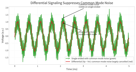
Fundamentals of Differential Signaling
Differential pairs consist of two complementary traces (positive and negative) that propagate signals with opposite polarities. The receiver subtracts the negative from the positive to recover the original data. This subtraction cancels out noise picked up equally on both traces, such as from power supply fluctuations or external interference. In PCB terms, the key parameter is differential impedance—typically 90–100 ohms depending on the standard—which must remain consistent along the entire path to avoid reflections.
Why Differential Pairs Are Essential Today
Data rates have risen dramatically in modern devices, from 480 Mbps in USB 2.0 to 20 Gbps per lane in PCIe 5.0. Single-ended signaling struggles with noise and skew at these speeds, leading to bit errors. Differential pairs tolerate longer trace lengths and harsher environments while emitting less EMI. They have become standard in consumer electronics, automotive infotainment, and data centers where signal integrity directly impacts performance.
Key Advantages and Common Standards for Differential Pairs
Benefits Over Single-Ended Signaling
Differential pairs offer several practical advantages. They provide excellent common-mode rejection, often 20–40 dB better than single-ended lines, which reduces susceptibility to ground bounce and crosstalk. EMI emissions drop because the opposite currents cancel magnetic fields. Return currents stay confined between the pair and its reference plane, minimizing loop area. In noisy environments like automotive or industrial systems, these benefits translate to lower bit error rates and more robust links.
Popular Standards and Typical Impedance Requirements
Most high-speed interfaces specify differential pairs with tight impedance tolerances. Common examples include:
| Standard | Typical Differential Impedance | Data Rate Example | Notes |
| USB 2.0/3.0 | 90 Ω ±15% | 480 Mbps / 5 Gbps | Full-speed and SuperSpeed |
| HDMI 1.4/2.0 | 100 Ω ±10% | Up to 18 Gbps | TMDS pairs |
| PCIe 3.0/4.0 | 100 Ω ±10% | 8–16 GT/s per lane | High tolerance for reflections |
| 1000BASE-T Ethernet | 100 Ω ±10% | 1 Gbps | Twisted pair emulation on PCB |
Table 1: Common differential pair standards and impedance targets.
These values come from interface specifications and require controlled dielectric materials and trace geometry during fabrication.
Essential Design Rules for Reliable Differential Pairs
Impedance Control, Width, Spacing, and Length Matching
Differential impedance is calculated using trace width (W), spacing (S), height to reference plane (H), and dielectric constant (Er). For a typical 100 Ω pair on FR-4, widths of 4–6 mil with spacing 5–8 mil and prepreg thickness 4–6 mil work well. Field solvers like Saturn PCB Toolkit or built-in calculators in Altium/KiCad provide precise values based on stackup. Variations in etching or dielectric can shift impedance 5–10%, so specify tolerances in fabrication notes. Length matching limits intra-pair skew to 5–15 ps (depending on rise time)—use accordion or sawtooth patterns on the longer trace, keeping amplitude low (<3x width) to avoid added inductance or capacitance.
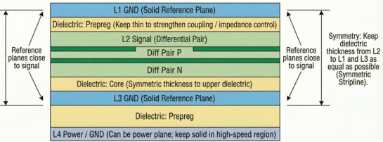
Reference Planes, Return Paths, and Layer Selection
A continuous reference plane (preferably ground) immediately adjacent to the pair is essential for stable impedance and low inductance return. Splitting planes forces return currents to detour, creating common-mode noise. In multilayer designs, prefer inner layers for shielding from external interference, but ensure the stackup is symmetric to control warpage during lamination. For high-layer-count boards, alternate signal and plane layers to provide multiple references. Stitching vias every 5–10 mm around the pair perimeter tie planes together across layers.
Advanced Routing Techniques and Signal Integrity Practices
Coupling Strategies, Via Handling, and Crosstalk Reduction
Tight coupling (S ≈ W) maximizes common-mode rejection but lowers impedance; loose coupling raises impedance for easier matching. Route pairs with constant spacing and avoid sharp bends—use 45-degree angles or arcs with radius >3x width. For vias, minimize stubs by back-drilling or using blind/buried vias; place pair vias symmetrically and surround with ground vias (4–6 per pair) to maintain shielding. Keep pairs at least 5H (height to plane) away from aggressors to limit far-end crosstalk below -40 dB
Simulation Tools and Manufacturing Considerations
HyperLynx or SIwave for pre- and post-layout simulation reveal eye closure or reflections early. TDR testing verifies impedance continuity. Manufacturing factors like copper roughness (low-profile foil preferred), solder mask thickness, and etch uniformity affect loss and skew. Controlled processes achieve ±8–10% impedance accuracy, with test coupons on panels for verification. DFM rules include avoiding acid traps in tight spacing and ensuring minimum drill-to-copper clearance for reliable plating.
Common Challenges in Differential Pair Design and How to Overcome Them
Impedance Discontinuities, Skew, and EMI Issues
Bends, connectors, or layer changes create impedance drops, causing reflections that degrade eye openings. Excessive intra-pair skew converts differential to common-mode, increasing EMI. Solutions include gradual tapers at transitions, tight length tolerance (<0.1 mm for >5 Gbps), and shielding with ground pours or vias.
Role of Professional Fabrication in Resolving Tolerances
Etch variation and dielectric inconsistency can shift impedance 10–15%. Professional fabricators use laser direct imaging for precise patterning, controlled prepreg flow, and impedance coupon testing to hold ±5–10% accuracy. They also optimize stackup for low-loss materials and provide early DFM feedback on via structures or spacing feasibility.

Conclusion
Differential pairs are critical when data rates exceed 1 Gbps, noise margins tighten, or EMI compliance is required—common in modern interfaces like USB-C, PCIe, and high-resolution video. Proper implementation ensures open eyes, low BER, and certification passage.
For reliable results, partner with a fabricator experienced in high-speed boards. JLCPCB offers precise impedance control (±10% standard, tighter on request), multilayer and HDI support for dense routing, and quick-turn prototyping to validate signal integrity early. Their online calculator and DFM checks help refine differential pair parameters before production. Upload your design at jlcpcb.com for instant quoting and fabrication that meets demanding high-speed requirements.

FAQ: Common Questions About Differential Pairs
Q1: What is the main difference between differential and single-ended signaling?
A: Differential uses two complementary traces to cancel common-mode noise, offering better immunity (20–40 dB) and lower EMI than single-ended, which relies on a single trace and ground reference.
Q2: How tight should length matching be for differential pairs?
A: Keep intra-pair skew under 5–15 ps (or <0.1 mm for >5 Gbps signals) to prevent timing errors and mode conversion—use serpentine routing on the longer trace.
Q3: Why is a solid reference plane critical for differential pairs?
A: It ensures consistent impedance, low-inductance return paths, and shielding; plane splits force current detours, creating noise and discontinuities.
Q4: Can I route differential pairs on outer layers?
A: Possible but not ideal—inner layers provide better shielding and impedance stability; outer layers increase susceptibility to external noise and require extra guarding.
Popular Articles
Keep Learning
How to Choose and Place Decoupling Capacitors for PCB Design
Every digital PCB depends on decoupling capacitors, yet a surprising number of boards still suffer from voltage dips, glitches, and electromagnetic interference (EMI) issues caused by one simple mistake: incorrect placement or selection. This guide walks through what decoupling capacitors do, how to choose the right value, where to place them, and which layout mistakes to avoid, so your next board runs clean on the first try. Key Takeaways Place one decoupling capacitor near each IC's power pin. Use 1......
Understanding DC 5V Input in PCB Design: Key Considerations
Note Correct Input: Power 5V through USB or header pins, as barrel jacks require at least 6.5V. Trace Sizing: Use 1.3mm traces on 1oz copper for 2A loads to keep voltage within 5%. Regulator Choice: Use LDOs for low-current analog circuits and Buck regulators for loads over 1A. Thermal Design: Place 0.3mm drill thermal vias on a 1.0mm grid under power ICs. Input Protection: Safeguard 5V inputs with a 5.6V TVS diode and a PPTC resettable fuse. DC 5V input is a critical aspect of PCB design, ensuring vo......
Optimizing Power Nets for Stable and Efficient High-Performance PCBs
Key Takeaways Power Nets as Systems: It is a complete copper network of planes, pours, traces, and vias built to deliver clean, stable voltage. Control IR Drop: Copper resistance causes voltage drop. Use wider traces, solid pours, or heavier copper (2 oz+) to stay within voltage tolerances. Minimize Loop Area: Place decoupling capacitors close to power pins with short, wide traces to handle fast transient currents. Scale Your Vias: A single 0.3mm via carries only 1 to 2A. High-current paths require pa......
Achieving Stable Power Delivery : Mastering PDN Impedance in High-Performance PCBs
Key Takeaways PDN impedance directly determines voltage stability under load. Keep it low and flat. Calculate your target: Z_target = (V_dd × Ripple%) / I_transient — typically single-digit milliohms. Prioritize close power-ground planes, short via connections, and strategic decoupling placement. Avoid anti-resonance peaks; a smooth curve matters more than raw capacitance. Precise manufacturing (copper thickness, dielectric control) is essential to match simulation results. There's no point in using a......
Phase Matching in High-Speed PCB Design: Achieving Signal Integrity with Precision Manufacturing
Key Takeaways Phase matching controls electrical trace length in high-speed PCBs to maintain precise signal timing and phase relationships. Even 10–15 ps skew (roughly 1–2 mm difference) at 10 Gbps can collapse eye diagrams, raise bit error rates, and cause system failures. Dynamic phase matching maintains alignment throughout the entire signal path, accounting for bends, vias, and layer transitions. USB 3.x SuperSpeed interfaces commonly target intra-pair skew below 5 mils (0.13 mm) to maintain relia......
Mastering Split Planes for Cleaner Power Delivery and Better Signal Integrity
Key Takeaways Split power planes when needed for multiple voltage domains or analog/digital isolation, but never split ground planes — always keep ground continuous for clean return paths. Avoid routing high-speed signals across splits; if unavoidable, use stitching capacitors (0.1 µF) and ensure differential pairs cross together. Place split power planes next to a solid ground layer, maintain ~10 mil moat width, and use proper decoupling near IC pins. Good split plane design significantly reduces noi......